Scattering of graphene plasmons at abrupt interfaces: an analytic and numeric study
A. J. Chaves1, B. Amorim2, Yu. V. Bludov1,
P. A. D. Gonçalves3,4, N. M. R. Peres11Center and Departament of Physics, and QuantaLab, University of Minho, Campus of Gualtar, 4710-057 Braga, Portugal
2CeFEMA, Instituto Superior Técnico, Universidade de Lisboa,
Av. Rovisco Pais, 1049-001 Lisboa, Portugal
3Department of Photonics Engineering and Center for Nanostructured
Graphene, Technical University of Denmark,
DK-2800 Kgs. Lyngby, Denmark
4Centre for Nano Optics, University of Southern Denmark,
Campusvej 55, DK-5230 Odense M, Denmark
Abstract
We discuss the scattering of graphene
surface plasmon-polaritons (SPPs) at an interface between two semi-infinite
graphene sheets with different doping levels and/or different underlying
dielectric substrates. We take into account retardation effects and
the emission of free radiation in the scattering process. We derive
approximate analytic expressions for the reflection and the transmission
coefficients of the SPPs as well as the same quantities for the emitted
free radiation. We show that the scattering problem can be recast
as a Fredholm equation of the second kind. Such equation can then
be solved by a series expansion, with the first term
of the series correspond to our approximated analytical solution for
the reflection and transmission amplitudes. We have found that almost
no free radiation is emitted in the scattering process and that under
typical experimental conditions the back-scattered SPP transports
very little energy. This work provides a theoretical description of
graphene plasmon scattering at an interface between distinct Fermi levels
which could be relevant for the realization of plasmonic circuitry
elements such as plasmonic lenses or reflectors, and for controlling
plasmon propagation by modulating the potential landscape of graphene.
††: jopt
1 Introduction
Controlling the propagation of graphene surface plasmon-polaritons
(SPPs) [1, 2, 3] is an important technological
problem for applications in SPP circuitry [4, 5].
It is well known from elementary wave mechanics that any wave will
be both reflected and transmitted at an interface where the properties of the propagating
medium change. The situation is no different with graphene SPP in
the presence of a spatial change of graphene’s conductivity and/or
dielectric properties of the surrounding media.
The possibility of generating interfaces for the reflection of graphene
SPP by changing graphene’s conductivity is particularly attractive
for the construction of tunable graphene SPP-based circuitry elements,
such as reflectors and beam-splitters, due to the possibility of controlling
graphene’s doping level. In a graphene field effect transistor, the doping
of the system is controlled by the gate voltage and by the dielectric
between graphene and the gate electrode [6, 7].
Therefore, a possible way to create a conductivity interface is to use
a graphene field effect transistor with two different dielectric substrates
below the graphene layer, as depicted in figure 1.
Due to the different local capacitances, different electronic densities
will be induced in the two graphene regions, which in turn implies
a different optical conductivity for the two regions. Other possibility
is to consider a single dielectric as the graphene substrate, but
using a split gate geometry, such that the applied gate voltage can
be independently controlled in two different regions [8].
A spatial modulation of graphene’s doping level could also be achieved
via non-uniform chemical doping. In general, a graphene SPP incident in a
conductivity/dielectric interface will be partially transmitted and partially
reflected. Once the problem of plasmon scattering at a single interface
is solved, it poses no difficulty to create a SPP filter by combining
three different dielectrics in sequence, thereby generalizing the
scheme of the device depicted in figure 1.
It should be noted the scattering of a SPP at an interface involves not
only the transmission and reflection of the field as SPP, but also
the emission of free radiation[9, 10].
Ideally, one would want this emission of radiation to be as small as possible
in order to keep the energy within the SPP wave. As we shall see ahead,
under typical experimental conditions, we predict that the losses in the
scattering event via emission of free propagating radiation are minute.
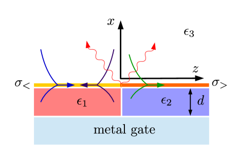
Figure 1:
Illustration of the geometry considered for the SPP scattering problem.
The yellow and red lines stands for graphene at two different electronic
densities. For simplicity we assume that the electronic density changes
abruptly at , in a step-like manner. We allow for different
dielectric substrates in the regions . The presence of a metallic
gate allows the tunning of the doping level of the graphene layer.
A typical SPP scattering event is represented:
a SPP impinging from the left at the interface can both be reflected and
transmitted as a SPP, or scattered into free radiation.
In this work we study the scattering of
a graphene SPP at normal incidence by a conductivity and/or dielectric
interface. The scattering problem is treated by expanding the electromagnetic
field in terms of a set of local eigenmodes and then using wave matching
at the conductivity/dielectric interface. This method takes into account
both retardation effects and emission of free radiation. Analytic, approximate
expressions are obtained for the graphene SPP reflection and transmission
coefficients. The approximate solution is compared to a numerical solution
of the wavemathcing problem. It is worthwhile pointing out that the problem of reflection
of graphene SPPs at a conductivity step was previously studied
in Ref. [11] employing a fully numerical method, but in
the electrostatic limit, which does not take into account radiation losses.
The problem of reflection at a conductivity interface for non-normal incidence
was studied in Ref. [12], also in the electrostatic limit.
The scattering of graphene SPPs by a conductivity barrier/well has
been considered in Ref. [13], taking into account retardation
effects in a fully numerical approach. In addition, the reflection of SPP at a graphene
edge was studied in Ref. [14]. Research on graphene
plasmonics is a relatively recent topic [1] and research
on graphene plasmonic circuitry is still in its infancy. We note,
however, that imaging of graphene plasmon scattering on lattice defects [15, 16]
and corrugations [17] has already been reported.
It is also worthwhile noticing that the experimental study of scattering
of SPP in metals has also been reported in Refs. [9, 18, 19, 20]
and the generation of unidirection SPP beams was reported in Ref. [21].
On the theoretical side, the problem of scattering of SPP in metals
by one dimensional defects, such as wires or grooves, has been studied
in Refs. [4, 10, 22, 23, 24, 25].
Finally, the scattering of phonon-polaritons at dielectric interfaces has been
studied in Ref. [26].
This paper is organized as follows: in section 2 we
define the problem and lay down the general approach to tackle it based
on a local eingenmode expansion of the electromagnetic field and wave
matching. We describe
the electromagnetic mode structure and dispersion relations, considering graphene SPP, waveguide and free radiation
modes. Section 3 is devoted to the problem of graphene
SPP scattering. In section 3.1, we solve
the scattering problem analytically
in the approximation of weak coupling of SPPs to radiation modes;
in section 3.2 we show that the scattering
problem can be recast as a Fredholm equation of the
second kind. We show that the approximate results can be
recovered from the zeroth order solution of the Fredholm equation in section 3.2.1.
We compare the analytical results with a numeric solution of the Fredholm equation and discuss the obtained results
in section 4.
Conclusions are drawn in section 5.
2 Geometry and electromagnetic modes
The scattering problem and the geometry we discuss in this work is represented
in figure 1. An identical geometry has been considered
in the case of scattering of surface phonon-polaritons
[26].
We assume a plasmon propagating from the left at normal incidence, that is, along the
axis. When impinging at the interface between the dielectrics
and , part of the plasmon will be reflected, part
will be transmitted, and some of the energy will be radiated to the far field.
We assume a time dependence of the electromagnetic fields of the form
.
We obtain the electromagnetic modes of the fields in the geometry depicted in
figure 1 by solving Maxwell’s equations
(see A). The resulting
modes are labeled by an index . The properties of these modes are analysed
in detail in this section. We make a piecewise decomposition of
the fields in terms of the eigenmodes,
using the superscript () for the () region:
(1)
(2)
where is the wavenumber of mode along the direction,
indicates a left/right propagating wave and
are mode amplitudes.
We clarify that the sum over actually denotes a summation over discrete
modes and an integration over continuum modes.
From A the eigenmodes of the component of the
magnetic field read:
(3)
where , and are constants to the later defined,
the graphene layer is located at and the metallic gate at , we have written
for the , regions, respectively, and
for each region, the wavenumber along the direction is given by
(4)
with denoting the wavenumber in vacuum. The relation
between the wavenumber
and the frequency needs to be calculated for each mode, usually by
solving a transcendental equation.
In each region , the magnetic modes can be chosen to satisfiy the
orthonormality condition (provided there are no losses, i.e. or purely real dielectric functions and a purely imaginary
graphene conductivity)
(5)
where gives the component of the electric field for mode (see A).
From the boundary conditions on the graphene layer, , we obtain the following equations for ,
and
(6)
(7)
The solution of the above equations determines the spectrum and the
structure of the electromagnetic modes of the system. The
wavenumbers and can be real or
purely imaginary. From these possibilities we can classify the modes as:
graphene SPP (both and are real),
waveguide modes ( is imaginary and is real)
and free radiation modes (both and are imaginary).
As we do not want to discuss the decay of the modes as they propagate,
but only the scattering event at the interface, we will neglect losses.
In particular, we neglect the real part of the graphene conductivity,
which we model within a Drude model, by approximating
where
(8)
and assume the dielectric constants to be real valued.
2.1 Graphene SPP
The graphene SPP is a mode localized in the graphene layer. Further
in the paper we will denote the graphene SPP mode by index .
It is characterized by real and .
The fact that is real, forces us to set
to zero in equations 6 and 7,
in order to avoid the unphysical situation of the field growing
exponentially when . This leads to the following implicit condition for the
graphene SPP dispersion
relation
(9)
Clearly, when we recover the dispersion relation
of plasmons in a graphene layer clad between two semi-infinite dielectrics [1].
We fixe by imposing the normalization condition
(10)
leading to
(11)
Approximate solution for graphene SPP dispersion relation
In the electrostatic limit (), we approximate
. With this approximation
equation 9 becomes
(12)
Using 8, we can solve the previous equation for obtaining
(13)
where we have introduced the fine-structure constant .
In the limit of a thick substrate , we approximate , recoverying the
dispersion relation for a surface plasmon-polariton in graphene supported by an infinite dieletric
(14)
with the characteristic dependence.
In the opposite limit, , we approximate and obtain
(15)
and we obtain a linear dispersion relation for small wavenumbers.
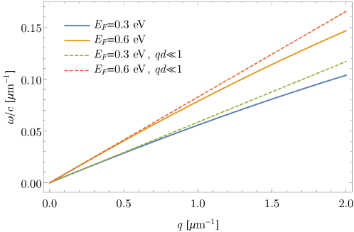
In figure 2 we show the dispersion relation of the SPP for
two different Fermi energies. It is clear that for typical substrate tickness and wavenumbers,
the dispersion relation is closer to linear than to the square root dependence.
Figure 2:
Dispersion relation of graphene surface plasmon-polariton 13
for two different Fermi energies:
eV (solid blue line) and eV (solid yellow line).
Also represented are the small wavenumber approximations 15 for the
plasmon dispersion relation (dashed lines).
The values used in the plot are nm, and .
2.2 Waveguide modes
In the case where , the structure supports
modes which are localized in the region , dubbed waveguide modes.
Waveguide modes are oscillating in the region, but decay exponentially
for . As in the case for graphene SPP,
is real and thus we set . However, due to the
oscillating nature of the field for ,
is now purely imaginary. The dispersion relation of the waveguide
modes is still given by equation 9, but with imaginary
. Namely, we obtain the condition
(16)
The solutions for this equation are organized as a
series of bands with discrete spectrum, ,
restricted to the region
,
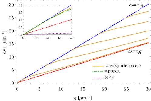
as it is shown in figure 3
for a typical setup. As it can be seen from the figure, the lowest, ,
waveguide mode bifurcates from the origin and exists for all positive and
, while the remaining modes waveguide modes, , bifurcate
from the points with frequencies ,
lying on the light-line in vacuum and existing in the spectral range
above those frequencies, .
The presence of the graphene has a negligible influence on the
spectrum of the waveguide modes for the parameters considered.
Figure 3: Dispersion relation, ,
(solid yellow lines) for the first five waveguide modes for
a structure with nm, , , and eV. The dispersion relation
for the waveguide modes in the absence of graphene is indistinguishable from the dispersion shown on the scale used
The light-lines , with are shown for
(blue dashed line) and (red dashed line).
Inset: Zoom in the region with from to . The dispersion relation of
the graphene surface plasmon polarion is shown by the dotted purple line, and the
approximated dispersion relation for the waveguide mode 18
is represented by the dot-dashed green line.
Approximate dispersion relation for the lowest waveguide mode
In the limit of small frequency and momentum, and neglecting the effect
of the graphene layer, it is possible to obtain an approximate expression
for the lowest, , waveguide mode dispersion. Neglecting the graphene
conductivity term in equation 16 and
approximating , we obtain
the following condition
(17)
Recalling the definitions of
and ,
the previous equation can be solved to lowest order in , leading
to the approximate dispersion relation for the waveguide mode
(18)
This approximate expression for the dispersion relation of the lowest
waveguide mode is shown in figure 3.
It is clearly seen that for the parameters of figure 3
this approximation is valid for
and fails for larger wavenumbers.
2.3 Radiative modes
Besides localized modes (SPP and waveguide), there is a
continuum of radiative modes. Radiative modes are characterized
by .
We chose to label these modes by their frequency, , and
momentum along the direction in the region , , which
we can choose to be positive, such that . In this situation, we obtain
where we have substituted the index by .
Equation 19 corresponds to the dispersion relation
of the radiative modes. The aforementioned positiveness of results
in the fact that the dispersion relation of these modes lies above the light-line for
a dielectric with (see figure 3).
Notice that for the radiative modes are actually
evanescent waves along the direction with imaginary . Therefore, it is with some abuse of language that
we refer to them as radiation modes. On the other hand, for , is real and we wave a true radiation mode
corresponding to a propagating wave in both the and directions.
Both kinds of modes are necessary when
making the mode matching at the interface . We also have that
is real for
(see equation 20), thus describing evanescent
waves along direction, in the substrate with dielectric constant
; and is imaginary in the opposite situation ,
which corresponds to the propagating wave along the direction in the
substrate (when waves for any
are of that type). For radiation modes all the coefficients
, and in equation 3
are non-zero. Imposing the boundary conditions at the interface (see A) we can
write and ,
as
(21)
(22)
where we have defined
(23)
(24)
The electric and magnetic field modes, can thus be written as
(25)
and the corresponding component of the eletric field reads
(26)
The modes can be normalized through the condition:
(27)
which fixes to have the value
(28)
Notice that will be imaginary when is imaginary.
3 SPP scattering
We now consider the problem of scattering of a graphene SPP which
is illustrated in figure 1. A plasmon coming
from the left and impinging at the dielectric/conductivity interface at
is scattered into both a back-scattered (reflected) and
forward-scattered (transmitted) plasmon, and also into free propagating
radiation. For simplicity, we will
consider a situation where no waveguide modes are supported ().
In order to determine the total field in the regions ,
we must consider both the discrete plasmon mode and the radiative modes.
Therefore the expansion of the electric and magnetic fields in terms
of local eigenmodes, equations 1 and 2,
reads for (note the phase of introduced in the reflection coefficients of the electric field)
(29)
(30)
while for we write
(31)
(32)
In these expressions, and are,
respectively, the reflection/transmission amplitudes for the SPP and
radiative modes with wavenumber along the direction, for . The relation
between the frequency and the in-plane graphene SPP momentum,
, is determined by equation 13.
Performing mode matching by enforcing the continuity of and at , we obtain the set of equations
(33)
(34)
Note that in order to satisfy the matching conditions at , we need both propagating
and evanescent radiative modes along the direction.
To determine the reflection and
transmission amplitudes, we take the inner product (as defined in 5) of 33 with
and , and the inner procuct of 34 with
and . Using the orthonormality
of the modes, we obtain the following system
of equations
(35)
(36)
and
(37)
(38)
The solution of this system of coupled integral equations
yields the reflection and transmission amplitudes.
In the following, we will provide both an approximate analytic solution
and a full numerical solution for this system of equations.
3.1 Approximate analytical solution
In order to proceed analytically, we will introduce some approximations.
We assume that the following relations hold [26]
(39)
(40)
Mathematically these relations mean that the modes of the different
regions are almost orthogonal. Physically, we can
understand this as a statement that the SPP modes are weakly coupled
to the radiation modes. The previous relations
are approximately true as long as
and .
This regime implies small
reflection amplitudes, as can be seen in figure 4. However, as we
will see below, the approximation performs well even beyond this
regime. With the aforementioned approximations, equations 35 and 36
become
(41)
(42)
We have thus obtained a closed set of two equations for the SPP reflection
and transmission coefficients. Solving these, we obtain
(43)
(44)
The transmission and reflection coefficients for the radiative modes can
be obtained from equations 37 and 38 if
we use the approximation 40, while keeping
and (in order to
obtain a non-zero result). We obtain the following equations
(45)
(46)
Using the previously obtained value for , we can solve for
and , yielding
(47)
(48)
The inner products in the above equations can be computed analytically
and explicit expressions are given in C.
One comment regarding the validity of the employed approximations
is in order. Notice that instead of contracting equations 33
and 34 with and ,
as done to obtain equations 35 and 36,
we could have contracted them with and .
Such a procedure would lead to the following equations
Solving these equations, gives us the alternative expressions for the reflection
and transmission coefficients
(53)
(54)
Since and can be chosen
as real, we conclude that equations 43 and 53
for coincide. However, we see that equations 44
and 54 differ by a factor of .
This gives us an internal consistency check for the employed approximations:
they remain valid as long as
(55)
which implies a strong coupling between the SPP modes from and for .
Note that the value for obtained with these approximations is
purely real. Therefore there is no phase-shift in the back-scattering
amplitude of the plasmon, except for the already included phase-shift
of . This is a consequence of the approximation introduced above
and contrasts with the results of
[11, 14], obtained within the electrostatic limit,
thus ignoring retardation effects.
It should also be noted that the formalism is capable of describing the reflection
of a graphene plasmon at the edge of a semi-infinite graphene sheet.
We have verified numerically that in this case the transmittance is
numerically very small (due to the approximations is not exactly zero)
and the reflectance is essential equal to unity (results not shown;
numerically we take the Fermi energy at the right of a very
small number, typically , as the numerical procedure
does not allow a zero Fermi energy).
In Ref. [11], an electrostatic calculation predicts that
the reflection coefficient for graphene in vacuum and subject to a
conductivity step at is given by
(56)
If we use the numbers of figure 4 for the Fermi energies
and plug-in the corresponding wavevectors in formula 56
we obtain the value , whereas
our calculation in the same conditions predicts a value in the range
, as the frequency of the
incoming SPP ranges from zero to 16 meV. Note that a consequence of the electrostatic approximation is
that the reflection coefficient becomes frequency independent. When taking the electrostatic
limit, we can study two possible cases: (i) thin substrate limit,
, and (ii) thick substrate limit, .
In the electrostatic and thin substrate limits () the reflectance amplitude 43 reads
(57)
in agreement with the result of Ref. [11] for
.
For the transmittance amplitude 44, and in the same limit as before, we obtain
(58)
Physically, the limit means that the plasmon fields
are finite only in the dielectric , as the field is
screened by the metallic gate. We also note that equations 57
and 58 contain the limit of total reflection when
. As anticipated, it is possible to have SPP
reflection even if if ,
provided that and differ.
Conversely, in the electrostatic and thick substrate limits (,
), we obtain for 43 and 44
(59)
(60)
3.2 Formulation as a Fredholm equation
We will now recast the scattering problem in a form ameable to a numerical solution. While doing that, we will see how the
approximate analytic result corresponds to a lowest order approximation to the solution of the complete problem.
Recalling equations 35-38 and
subtracting equation 36 from equation 35, we obtain
(61)
Furthermore, subtracting equation 38 from equation 37, we obtain
(62)
Combining equations 61 and 62
we eliminate and obtain a closed equation for the reflection
coefficients
(63)
where we have introduced the quantities
(64)
(65)
Equation 63 is in the form of a Fredholm integral
equation of the first kind. However, as shown in the C,
the integration kernel contains a term that
is proportional to a -function (see equations 134
and 135). Therefore, we can split
as
(66)
where is the diagonal part of , with its
explicit form given in equation 147, and we
have written the remaining part as . Inserting
this equation into equation 63 and using the -function
to perform the integration over , we can transform the
problem into a Fredholm integral equation of the second kind, as
(67)
This equation can be solved numerically, by discretizing the integral over using a Gaussian quadrature method,
and evaluating the equation for values of on that same discretized grid, reduzing the integral equation
to a problem of linear algebra as described in greater detail in D.
Having obtained the reflection coefficient , the reflection coefficient for hte
the SPP mode, , can be computed from equation 61.
With the knowledge of all the reflection coefficients, the transmission
coefficient can be calculated from equation 35 as
(68)
(69)
and the transmission coefficients can be determined from
equations 61 and 38 as
(70)
(71)
(72)
This provides a general scheme to fully solve the scattering problem.
Notice that
equations 61, 69,
and 72 can be rewritten as
(73)
(74)
(75)
with , , ,
and the analytical approximate results
given, respectively, by equations 43, 44,
47, and 48.
In the following, we will see how the approximate analytic result from
Sec. 3.1 can be recovered from a
lowest order solution to the Fredholm equation.
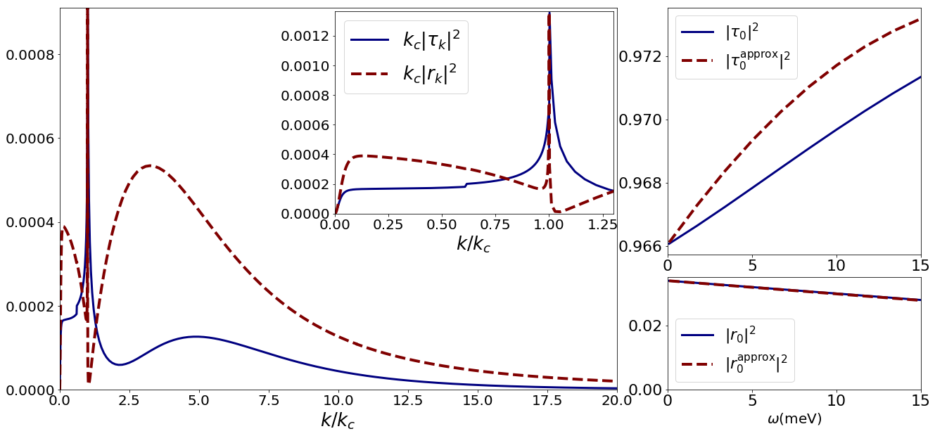
Figure 4:
Left panel: Transmittance and reflectance of the radiative modes as function of ,
in the interval , for meV.
The inset zooms in the interval .
Right panel: Transmittance (top right) and reflectance (bottom left)
of graphene SPP as a function of the plasmon frequency.
Both the results obtained with the analytic approximation (dashed purple)
and the full numerical solution (solid blue) are represented.
The difference
between the numeric solution of Fredholm equation and the approximated solution
for the reflection and transmission coefficients is smaller than 1%.
In both panels the used parameters are:
meV, nm, , , ,
eV, .
3.2.1 Recovery of the approximate analytical solution
We will now see how to recover the analytic result of
equation 47
from the lowest order approximate solution of the Fredholm
equation 67.
A possible strategy to solve the Fredholm equation,
is to employ an iterative method. Within this solution scheme, the
zeroth order solution is given by (see equation 67)
(76)
Now we notice that for
and , the quantity can be approximated as (see C)
(77)
Therefore, we can write the reflection coefficient as
(78)
Using equation 64 for , we recover equation 47,
that is, the analytical solution as the zeroth order term of the Fredholm equation:
(79)
We have verified numerically that the approximation given by equation 77
holds with great accuracy even if the conditions for its derivation are violated.
This explains the good results given by the analytic approximated solution,
even for relatively large contrast between the dielectric constants and the Fermi
energies.
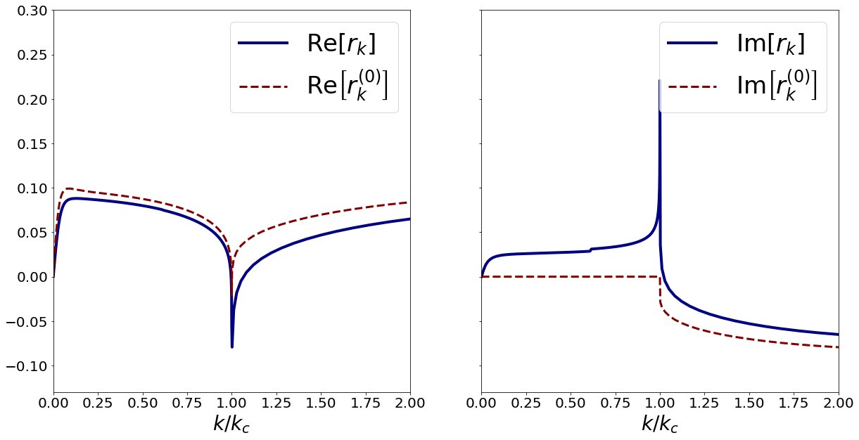
Figure 5:
Real (left panel) and imaginary (right panels) parts of the reflection coefficient (devided by )
obtained from the numerical solution of the Fredholm equation (solid blue line)
as a function of over the interval .
Also shown is the lowest order approximation to the reflection coefficient 76
(dashed purple line).
The parameters used are: meV, nm,
, , ,
eV, eV.
4 Results and discussion
We shown the reflection and transmission coefficients for the SPP, and , as a function of the plasmon
frequency, computed both with the analytic approximation (43 and 44) and with the numerical solution
of the Fredholm equation 67 on the right panel of figure 4.
As can be seen the, difference between both results is very small, not exceeding .
Notice however, that the approximated results overestimate the transmittance of the SPP, which is nevertheless very close to 1.
This implies that very little energy is either reflected as a SPP or lost due to emission of radiation.
This last statement is further confirmed by the smallness of the reflection and transmission coefficients
for radiation modes as shown as a function of (with )
on the left panel of figure 4.
Notice that the reflectance displays a significant dome for , highlight the importance of
radiation modes evanescent along the direction in the field matching at the interface at . In figure 5,
we shown the real and imaginary parts of the reflection coefficients obtained from the numerical solution of the Fredholm equation
and compare it to the lowest order solution as a function of . The agreement is reasonable for the real part, indicating that the
approximate analytic expressions indeed provide good results. However, in the imaginary part of the reflection coefficients
there is a significant discrepancy close to , with the numerical result displaying there a peak that is absent on the approximate result.
The validity of both the analytic results and the numerical solution can be accessed by studying the total scattered,
including the energy carried by the transmitted and reflected SPP and the energy radiated in the scattering process.
As a matter of fact, energy conservation implies that (see B), where
(80)
with
(81)
(82)
respectively, the energy radiated fraction of energy in reflection and transmission. Notice that the integration only goes up to ,
since modes with are evanescent along the direction, not carrying energy away for .
The statement simply means that the energy of the incident SPP is redistributed
into the reflected and transmitted SPP modes and into radiation modes
Notice that the approximate analytic results in the limits of and ,
57 and 58, imply that
that .
This means that in this is limit all the energy is carried by the transmitted and reflected SPP, with no radiation emission.
This is expected as in the electrostatic
limit no radiation can be emitted. However, in the limit of and
, equations 59 and 60,
imply that
(83)
Therefore, there
is a deviation from the ideal case, .
However, this deviation is small as long as ().
We must point out, however, that the term cannot
be identified with energy losses due to the emission of free
radiation, since in the electrostatic limit ()
the propagation of free radiation is forbidden. This deviation, is
therefore attributed to a limitation of the approximate analytical
result.
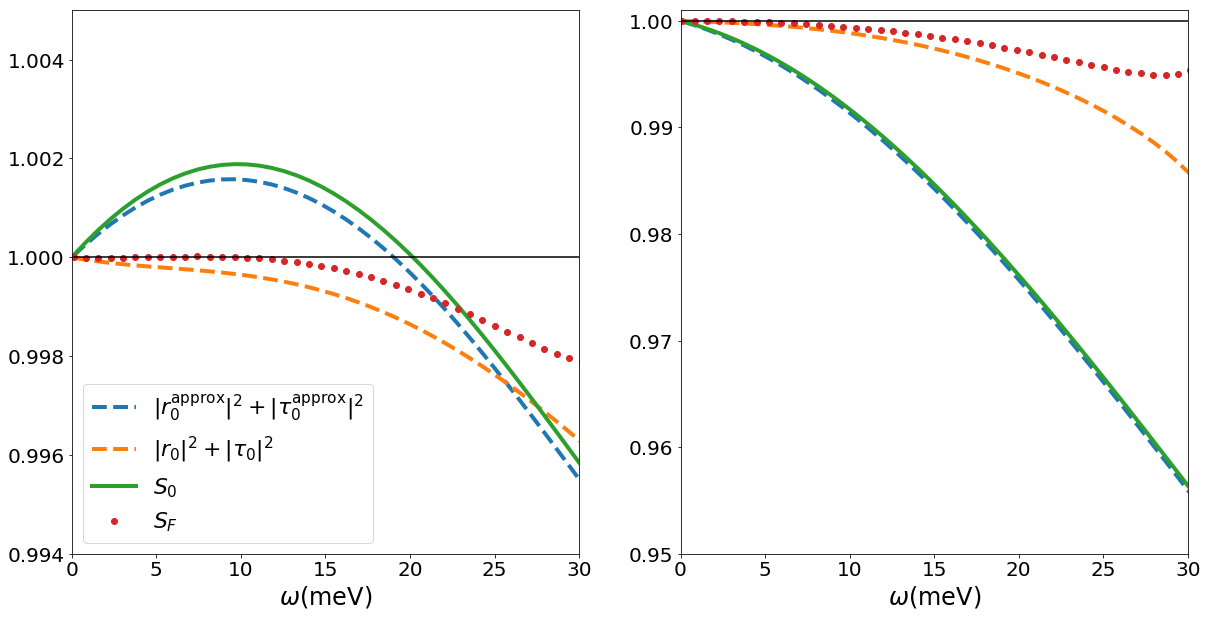
To check the conservation of energy as function of frequency, of both the approximate analytic and in the numerical results, we plot
in figure 6 the
energy sum, , as a function of the incident plasmon frequency in a range spanning 7.25 THz.
We see that the analytical results can violate the energy sum rule, leading to .
The analytical result can also lead to , which is clearly unphysical,
as it would correspond to a generation of energy. This indicates a limitation of the analytic approximation
which has also been reported in the scattering of surface phonon-polaritons
at the interface between two dielectrics [26].
Notice, however, that
the violation of the sum rule is actually very small, never exceeding (for eV and ).
The numerical solution of the Fredholm equation corrects the unphysical result and we recover
.
There is still a small violation of the sum rule which now lies bellow 1, due to errors induced by the
discretization of the integral in the Fredholm equation 67. However, the numerical solution
significantly improves the sum rule with the error being less than (for eV and ).
Notice that as we go to the sum rule, in both the approximate analytic
(which completely neglects radiation modes) and in the full numerical solutions (where the contribution
from the radiative modes is still subjected to errors due to the discretization of the integral),
is satisfied to a better degree. This is due to the fact that in the electrostatic limit the contribution due to
radiative modes becomes less important. The errors in both methods increase when the graphene conductivity contrast
is larger as can be seen on the right panel of figure 6
(results obtained for eV and ).
Since the sum rule is not exactly one, the fraction of energy emitted as radiation can be obtained from
, and can be seen to be extremely small,
but increases as the energy of the incident SPP increases and the graphene conductivity contrast is larger.
Figure 6:
Sum rule in a large frequency window.
The dashed lines refer to for the
approximation (blue) and the numerical solution (orange).
The green solid line refers to the approximated sum rule, , while the
red dotted line refers to the numerical
solution, . The parameters used are: nm, ,
, , eV,
eV. The right panel depicts the same quantities but for
eV, eV. The radiative correction is the difference between the orange dashed line and the red dotted one. We can see the
increasing of radiative emission for larger frequencies and higher Fermi energy mismatch.
5 Conclusions
We have analyzed in detail the scattering of graphene surface plasmon-polaritons
at a sharp graphene conductivity step and/or change of the dielectric
substrate. One of the merits of our calculation is the ability
to provide analytic expressions for the reflectance and transmittance
amplitudes for arbitrary values of the graphene sheet conductivity
and of the surrounding dielectric constants, in a realistic geometric
configuration. Although the analytical approach is not exact, it is
good enough to estimate the values of and , which can
be corrected either by an iterative solution or a fully numerical solution (see D)
of the Fredholm equation.
The corrections are, however, small. The calculation also predicts that the
emission of free radiation in the scattering event is small.
This situation is rather favorable for plasmon scattering,
as most of the energy remains in the plasmon field and is
not lost to the radiation continuum.
Note that our calculations are realistic
in what concerns the geometry of the system, since the metallic gate
is taken into account as is the existence of two different dielectrics
underneath graphene.
However, we assumed that the induced change of the graphene conductivity is abrupt at the interface.
A more realistic situation would be to consider a smooth transition
of the electronic density across the interface. In this case,
the reflection coefficients are no-longer well defined, except faraway
from the region where the conductivity changes; this renders the calculation
much more difficult. Nevertheless, our results should remain valid provided
the incident plasmon wavelength is much larger than the length scale over
which the graphene conductivity changes.
The method employed in this paper can be extended to
take into account the coupling of the SPP to the substrate’s surface
optical phonons, as for example in SiO2, by taking into account the
frequency dependence of the dielectric function of the substrate.
It is also possible to generalize the present method to a geometry
where a finite dielectric is sandwiched between two semi-infinite
ones. In this setup, by adjusting the length of the central dielectric it is possible
to achieve either total transmission or total reflection via Fabry-Pérot
oscillations, thus allowing the construction of a Bragg reflector.
Alternatively, we can change the value of the gate potential, thus tuning the frequency
for which there is total reflection or total transmittance. This give
us a real time and on-demand control on the scattering of the plasmon.
We point out that we have only focused on the case of scattering at normal
incidence. However, the method of eigenmode field expansion and matching
employed in this work can also be generalized and applied to the case
of oblique incidence. That extension will be the goal of a forthcoming
publication.
Acknowlegements
A. J. C. acknowledge the scholarship from the Brazilian agency CNPq
(Conselho Nacional de Desenvolvimento Científico e Tecnológico).
B. A., Y. V. B. and N. M. R. P. acknowledge support from the European
Commission through the project “Graphene-Driven Revolutions in ICT
and Beyond” (Ref. No. 696656).
P. A. D. Gonçalves acknowledges
financial support from the Center for Nanostructured Graphene,
funded by the Danish National Research Foundation (project DNRF103).
N. M. R. P. also acknowledges
the hospitality of the MackGraphe Center, at Mackenzie Presbyterian
University, where this work has started, the projects Fapesp 2012/50259-8
and 2016/11814-7, and the Portuguese Foundation for Science and Technology
(FCT) in the framework of the Strategic Financing UID/FIS/04650/2013.
Appendix A Eigenmodes of Maxwell’s equations
In this apendix we determine the eigenmodes of the system represented in figure 1
for each to the regions , by solving Maxwell’s equations
in this geometry. The electric, , and the magnetic , fields are governed by the inhomogeneous Maxwell equations
(84)
(85)
where is the current density due to the graphene layer at and is takes into account the inhomogeneous dieletric
environment that surrounds the graphene layer. is piecewise homogeneous and we write it as for
and for , with
(88)
(91)
The graphene current density is related to the eletric field by , where represents
the components of that are perpendicular to the direction. We also allow for different graphene conductivities
(due to different local doping levels) for and , respectively, and .
We will use the Drude model for the graphene conductivity, namely
(92)
with the local Fermi level and
the local decay rate.
We will consider that all fields have a harmonic time dependence
of the form and also assume that the system is translationally
invariant along the direction. We want to describe scattering at normal incident and therefore we can drop all depence of the problem on
the coordinate (i.e. ).
The total electromagnetic field can, in general, be split in two polarisations:
/TE (transverse electric) polarization and /TM (transverse
magnetic) polarization. Since the SPPs are TM-polarized waves, further
in the appendix we restrict our consideration to that particular polarization.
For this polarization and at normal incidence, the electric field will have non-zero and
components, ,
while the only nonzero component of the magnetic field is the component,
. Under these conditions
we rewrite Maxwell’s equations (84) and (85)
as
(93)
(94)
(95)
Due to the piecewise homogenity of the system along the direction, we can study separately
the electromagnetic fields in the regions and . In general, there is a
series of solutions, which we will refer to as eigenmodes, indexed by
some label for each of the regions . A general solution for each region can be
represented as a superposition of these eigenmodes. In particular,
the expression for the -component of the magnetic field at
have the form
(96)
while the nonzero components of the electric field are
(97)
(98)
are the eigenmode amplitudes and the summation is taken with respect to the eigenmode index .
The sign stands for the left/right
propagating waves in direction with wavenumber .
With some abuse of notation, the summation symbol in equations 96–98
actually represents a summation, an integral or both, depending if
the basis is discrete and/or continuous.
From equations 93-95, for each mode the functions , ,
and are solutions of the equations
(99)
(100)
(101)
As before, the piecewise-homogenity
of equations 99–101 along the direction
allows us to solve them separately in regions and
and then apply the boundary conditions. Thus, in the region ,
occupied by the dielectric substitution of equations 100
and 101 into equation 99
results into the wave equation
(102)
In the same way, for region , we obtain the wave equations
(103)
(104)
which are valid for the domains and ,
respectively. In equations 102–104
,
,
and ,
with the wavenumber in vacuum. Notice that
is the same in both and regions. The fact that we
have a perfect metal at forces the component of the electric
field to become null there. Therefore, the magnetic field mode along
the component must have the following form
(105)
with the component of the electric field given by
(106)
and the component being given by
(107)
Notice, that in equations 105–107
the subscript is for (and is combined with the superscript
), while the subscript is for (combined with the
superscript ). Also , and
are coefficients to be determined such that boundary
conditions at are satisfied and the mode is normalized. Integration
of equations 99-101
in the limits from to imposes the following
boundary conditions at
(108)
(109)
which translate into the following equations for ,
and
(110)
(111)
By solving these equations for and we obtain equations 21 and 22 of the main text.
The normalization condition 27 allows to fix the value of . By using the following results
Energy propagation is intimately related to the time average of the Poynting
vector , defined as
(115)
For a TM-polarized electromagnetic field propagating along the direction, the Poynting vector has the explicit form
(116)
In the presence of an imaginary-only conductivity energy is conserved
and Poynting’s theorem establishes that
(117)
where is the closed surface enclosing the volume
and is an infinitesimal areal vector lying on the surface
of and pointing from the inside to the outside of the
volume . We are interested in the fields in the far-field, therefore
we draw a cube passing through , , ,
and . As the fields do not depend on the integral
over can be reduced to a one-dimensional integral along
the rectangle defined by , , and .
We now use equations 29-32 to compute
the Poynting vector. The energy flow along the direction is related
to which reads
(118)
Integrating along the axis from
to and using the orthonormality of the modes it follows
that
(119)
In the far field the last term of the previous
equation is zero. In the same way the contribution from the surface
located at provides the result:
(120)
Finally, we still need the contribution from the line at .
The last term we need to compute is:
(121)
which corresponds to radiation emitted orthogonal to the graphene
plane. The plasmonic fields and go to zero when
and thus do not transport energy. Therefore we are
left with the term that depends on the radiative modes. It can be
shown that the integral is purely imaginary and therefore its real
part is zero and does not contributes to energy conservation. Putting
all together in equation (117) we find
(122)
which is the statement of energy conservation.
Appendix C Explicit form of the inner products
In this Appendix we list the explicit results for the inner products.
First we provide results for some useful integrals:
(123)
(124)
(125)
(126)
and
(127)
Using the previous integrals we can compute the different inner products,
which, after tedious calculations, read:
(128)
(129)
(130)
(131)
(132)
(133)
(134)
(135)
where we have defined the functions
(136)
(137)
where , , , and:
(138)
(139)
(140)
(141)
(142)
(143)
(144)
(145)
(146)
where in the last two equations, () for the superscript ().
From equations 134 and 135 and
from equation 64 and function , as defined by equation 66,
is given by
(147)
We point out that for and
we have that
(148)
such that we obtain
(149)
Appendix D Numerical solution of Fredholm Problem
To solve the Fredholm equation 67, first we introduce a cutoff in the integral, where is large
and is choosen as the value needed for the solution to converge.
The kernel of the Fredholm equation, , has a divergence of the kind:
(150)
that comes from the term proportional to in the inner products 134 and 135.
To regularize this divergence, we make the substitution:
(151)
where is a parameter choosen as small as necessary to achieve convergence of the calculation.
In the numerical results shown in the main text, we used and .
In the integral of equation 67 we make the variable change , and separate the integration limit in two parts:
(152)
Next, we divide each of those integrals in and equally spaced regions. For each of those regions, we apply a Gauss-Legendre quadrature
with (when ) and () points. The Fredholm problem now is transformed into a matrix equation:
(153)
where is a
matrix obtained from the discretization of the kernel , is the solution we seek, being a vector obtained by descritizing the
reflection coefficient, and is vector obtained from the discritization of the zeroth order solution of the Fredholm equation
76.
The solution of 153 is obtained trivially as .
For the results shown in this paper we used , , .
This numerical procedure works for the spectral range shown in this paper
(frequencies up to THz). For higher frequencies, the integration
of the resulting function, to calculate the sum rule 80,
diverges due to the singularity at the point (see figure 4).
To go to higher frequencies, a more sophisticated integration algorithm is necessary.
[15]
Fei Z, Rodin A S, Gannett W, Dai S, Regan W, Wagner M, Liu M K, McLeod A S,
Dominguez G, Thiemens M, Castro Neto A H, Keilmann F, Zettl A, Hillenbrand R,
Fogler M M and Basov D N Nat Nano (11) 821–825
URL http://dx.doi.org/10.1038/nnano.2013.197