Topological phases in Bi/Sb planar and buckled honeycomb monolayers
Abstract
We investigate topological phases in two-dimensional Bi/Sb honeycomb crystals considering planar, buckled, freestanding and deposited on a substrate structures. We use the multi-orbital tight-binding model and compare results with density functional theory methods. We distinguish topological phases by calculating topological invariants, analyze edge states of systems in a ribbon geometry and by looking at their entanglement spectra. We show that weak coupling to the substrate of buckled and planar crystals is sufficient to lead to a transition to the topological insulator phase. Topological crystalline insulator (TCI) phase exhibits a pair of edge states in the semi-infinite geometry and in the entanglement spectrum. Transport calculations for TCI phases show robust quantized conductance even in a presence of symmetry-breaking disorder.
keywords:
topological insulators, bismuth, antimony1 Introduction
Novel topological phases have gained an immense interest of both experimentalists and theorists in the current decade[1, 2, 3, 4, 5, 6, 7, 8, 9, 10]. They are attractive subjects due to potential technological applications in spintronic and quantum computing devices[11]. Topological insulators exhibit the energy gap inside the bulk and conduction channels at the edges, inherently protected against certain types of scattering. Quantum spin Hall (QSH) systems are two-dimensional (2D) representatives of the family of topological insulators protected by time-reversal symmetry[12]. The topologically nontrivial energy gap is opened by spin-orbit coupling (SOC), which is a characteristic of heavy elements. QSH systems were experimentally observed in thickness-tunable quantum wells and honeycomb-like systems based on groups of IV [13, 14, 15], II-VI [16, 17], III-V [18, 19, 20, 21, 22] and V [23, 24, 25, 26] elements including heavy atoms like bismuth or antimony. Recently, thin films of topological insulators protected by crystalline symmetries were recognized and dubbed topological crystalline insulators [6, 7, 8, 9, 10].
Bi and Sb crystals were extensively studied in the context of their topological properties. Murakami has predicted that Bi bilayer is topological insulators with characteristic helical edge modes propagating in opposite directions [23]. This was later confirmed experimentally by scanning tunneling microscopy measurements [27, 28, 29, 30]. Several authors investigated robustness of topological properties of Bi(111) and Sb(111) bilayers and few bilayer crystals[31, 32, 33, 34, 35, 36]. Sb(111) thin films with less than four bilayers were shown to be topologically trivial[25]. Transitions between topologically trivial and nontrivial phases can be induced by structure modifications involving chemical methods [37], artificial variation of spin-orbit coupling in Bi [31, 38], strain [26, 39, 40, 41] or interaction with a substrate[42, 43, 44, 30, 41]. Recently, TCI phase in flat Bi and Sb honeycomb layers was predicted [8]. In the presence of strain, buckled structures become completely flat, which leads to forming bismuthene (for Bi crystals) and antimonene (for Sb).
In this work, we investigate different topological phases in planar and buckled Bi and Sb two-dimensional honeycomb layers using multi-orbital tight-binding (TB) and compare results with density functional theory (DFT) calculations. We analyze whether TB method can be used as a complementary tool to characterize these crystals, as one of its advantage is studies of larger systems. We distinguish different topological phases for freestanding structures and deposited on a substrate. These phases are identified by computing topological invariants, looking at band structures in a ribbon geometry and analyzing entanglement spectra (ES). We focus mainly on characteristic features of TCI phase and study its topological protection against scattering by calculating conductance in a presence of crystal-symmetry breaking disorder.
The paper is organized as follows. In Section 2 we introduce the methodology. We compare tight-binding method with density functional theory calculations during buckled-flat transitions of freestanding systems in Section 3. In Section 4, we analyze the effect of the interaction with the substrate. In Section 5 we characterize topological phases using entanglement spectrum and in Section 6 transport properties of TCI phase are studied. We conclude the results in Section 7.
2 Methods
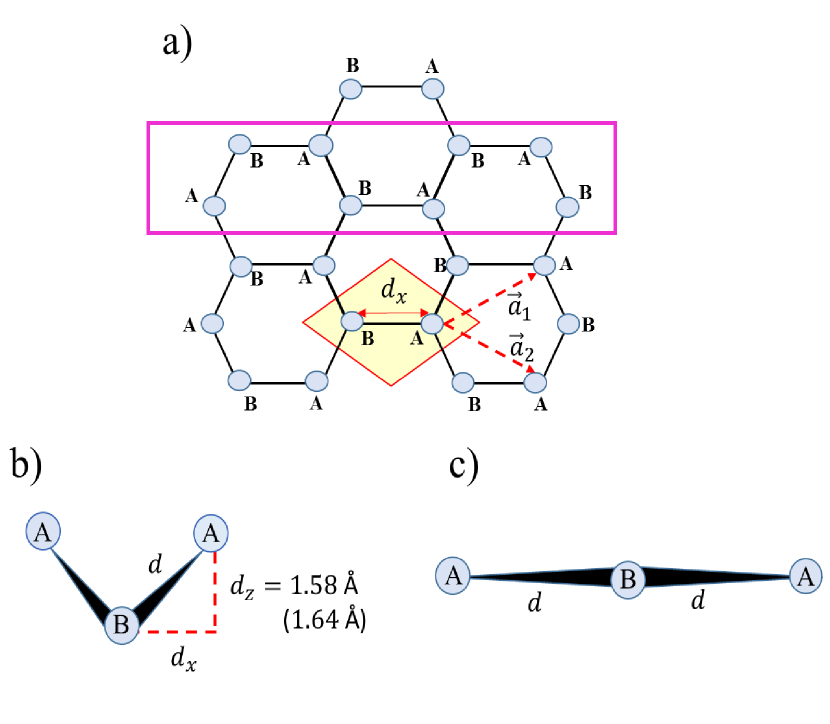
2D crystals Bi and Sb 2D are schematically shown in Fig. 1(a). A hexagonal unit cell contains two atoms, and . Freestanding Bi and Sb honeycomb layers have the lowest energy when two atoms are displaced in a vertical direction to a lattice plane, thus they are usually called bilayers [23]. While this displacement slightly differs in a literature depending on type of calculation[41, 45, 46], we take Å for Bi and Å for Sb. We will consider transitions between buckled Bi and Sb bilayers, Fig. 1(b), to flat honeycomb crystals, bismuthene and antimonene (see Fig. 1(c)), caused by an external uniform strain.
2.1 Tight-binding model
We use four-orbital () TB method with parametrization introduced by Liu and Allen [47] for bulk bismuth and antimony. The inter-atomic hopping up to the next nearest-neighbors and the atomic spin-orbit coupling (SOC) are parametrized with the Slater-Koster approach[48]. Therefore, we can write Hamiltonian as
| (1) |
where label orbital and spin degrees of freedom, denote atomic positions of the nearest (next-nearest II) neighbors to atom localized at . corresponds to the on-site energies and are Slater-Koster two-center integrals between and orbitals. The last term describes the spin-orbit coupling (SOC) with strength . TB parameters are listed in Table. 1. factor is introduced to renormalized atomic SOC strength in order to obtain correct SOC splitting of the valence band [49]. Buckled-flat transitions are modeled by linearly decreasing and at the same time linearly increasing lattice constants of Bi and Sb bilayers up to the values corresponding to completely flat bismuthene and antimonene, with Å and Å, respectively. According to Ref. [30], the SiC substrate is effectively described by shifting orbitals away from the low-energy sector.
| Parameter | Bi | Sb | Parameter | Bi | Sb |
|---|---|---|---|---|---|
| (eV) | (eV) | ||||
| Es | -10.906 | -10.068 | 1.854 | 2.342 | |
| Ep | -0.486 | -0.926 | -0.600 | -0.582 | |
| -0.608 | -0.694 | 0.156 | 0.352 | ||
| 1.320 | 1.554 | 1.5 | 0.6 | ||
| a (Å) | 4.53 | 4.30 | dz (Å) | 1.58∗ | 1.64∗∗ |
| dx (Å) | 2.62 | 2.48 |
2.2 Density functional theory
We study the atomic configurations and electronic properties of relaxed and strained 2D Sb and Bi crystals in the DFT framework. The DFT calculations are done within the generalized gradient approximation (GGA) and the Perdew-Burke-Ernzerhof (PBE) [52] exchange correlation function. The core electrons were model using the norm-conserving pseudo potentials. The cut-off energy for the plane wave expansion and charge density calculations are set to 75/85 and 750/850 Ry for Sb/Bi 2D layers. The distance between layers is 15 Å to avoid interaction between adjacent image layers. We apply the biaxial tensile strain which saves the hexagonal shape of the relaxed unit cell. The first Brillouin zone integration is performed in the Monkhorst-Pack algorithm [53] using a 15151 k-grid for relaxation of strained atomic configurations. In the relaxation, the total force on each atom in the final configuration is less than 0.001 (Ry/au). We start DFT relaxation from a completely flat structure and a buckled one to compare the final energy and find the lowest energy configuration. For band structure calculations which include the SOC, we used fully-relativistic pseudo potentials and a fine mesh of 25251 for k-grid. All DFT calculations presented in this article were performed using the Quantum-Espresso package [54].
The relaxed Bi and Sb honeycomb lattices are buckled and with lattice constants and Å, respectively. The equilibrium buckling of relaxed structures are 1.64 Å for Sb and 1.69 Å for Bi 2D planes. The resulted atomic configurations are in a good agreement with previous reports [55, 56]. Obtained values differ from chosen tight-binding parameters by less than , and we verify that this discrepancy do not affect results in a qualitative way.
2.3 Entanglement spectrum
Quantum entanglement measures have emerged as valuable tools in investigating topologically nontrivial phases of matter. Starting from a system in a ribbon geometry, we divide it into two spatially separated sub-regions denoted by and . The reduced density matrix for the region captures non-local correlations and can be represented in a form of , with being the normalization factor, since . is called the entanglement Hamiltonian, hence the entanglement spectrum (ES) is defined as a set of eigenvalues of denoted by . If the non-interacting fermionic system is considered, then is just the Hamiltonian restricted to the sites within the one subsystem.
For free fermion lattice systems, the reduced density matrix can be obtained from the one-particle correlation function [57]
| (2) |
where are lattice indices within the subsystem , correspond to orbital or spin degrees of freedom and the expectation value is taken in the ground state . If translational invariance is present in the system, the full Hamiltonian can be written in the momentum space and the many-body ground can be expressed in terms of Bloch states . Here is the conserved momentum and runs over the occupied bands. In that case the correlation matrix becomes -dependent, and therefore can be evaluated for each point in the Brillouin zone separately.
Correlation matrix can be regarded as a spectrally flattened physical Hamiltonian with eigenvalues , which are bounded by ’s and ’s. If system is in a topologically nontrivial phase, a continuous set of intermediate eigenvalues spectrally connecting ’s and ’s called the spectral flow is exhibited [58, 59]. Our aim is to observe whether distinct features between TI and TCI phases are observed.
2.4 Transport calculations
We consider two-terminal geometry with semi-infinite leads attached to the left and the right edge of the scattering region. We use the Landauer approach for the differential conductance , where is transmission matrix calculated using recursive Green’s functions approach, as explained in our previous work [31]. Disorder effects were introduced using Anderson model with on-site values chosen randomly from a uniform distribution (with being the disorder strength) and the conductance averaged over 100 samples with the different impurity realizations. All transport results were calculated for the nanoribbon scattering region size atoms without the inclusion of strain due to its negligible effect on a qualitative picture.
3 Comparison between density functional theory and tight-binding results for freestanding structures
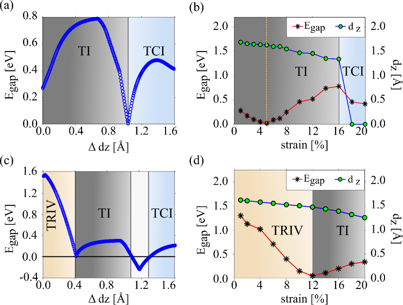
Methods within first-principles calculations are commonly used in order to study electronic properties of Bi and Sb honeycomb 2D crystals [23, 26, 27, 29, 30, 31, 32, 33, 34, 35, 36, 25, 37, 38, 39, 40, 41, 8]. We justify applicability of TB model by comparison results with our DFT calculations. We analyze the effect of biaxial strain leading to a transition between buckled and flat structures. Within TB method, bilayer structures correspond to , where with given in Table 1 and as a buckling for strained systems. Fig. 2 shows corresponding phase diagrams obtained within TB and DFT for Bi in (a) and (b), and for Sb in (c) and (d). The topological invariant is calculated from the parities of filled bands at four time-reversal invariant momentum (TRIM) points[3]. Qualitatively, phase diagrams look similarly within both methods. Unstrained Bi bilayer () is a TI[23, 50, 60, 42, 31]. A continuous change of within TB model leads to a transition to TCI phase, which occurs at Å and is expected in bismuthene [8]. Within DFT methods, we notice that after a critical value of strain, in this case, the system relaxes to the flat structure exhibiting TCI phase, which has the lowest energy. One can also notice the energy gap closing point around strain, however we verify that the system remains in TI phase. This is not observed in TB results. Agreement between phase diagrams obtained by TB and DFT methods is observed for Sb 2D honeycomb crystal. Strain induces a transition from a trivial phase to TI at around in DFT and at in TB, and to TCI phase for in TB, the phase expected for antimonene [8]. For TB results, a semi-metallic phase is observed between TI and TCI phases at around , however this corresponds to strain values inducing relaxation to a flat structure and thus is not seen in DFT calculations. The energy gap evolution within DFT results from Fig. 2(b) and (d) are also comparable with results from Ref. [26].
4 Substrate effect within tight-binding method
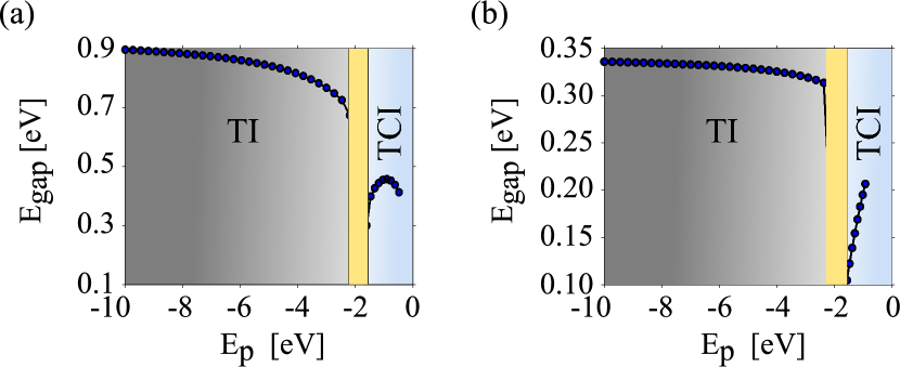
We investigate the effect of interaction between Bi and Sb 2D crystals with SiC substrate within TB method. Samples deposited on the substrate are coupled to it mainly through orbitals perpendicular to the layer, orbitals in this case. This can be modeled by shifting up the orbitals energy from a low energy sector [30]. We note that this effective model describing the substrate effect unable to determine correctly the Fermi energy at intermediate values of , when energy bands continuously shifts in energy with . We exclude the region from the phase diagram where the band consisted mainly of orbitals crosses the Fermi energy, the yellow areas in Fig. 3. In Fig. 3(a) and (b), energy gaps as a function of are shown for bismuthene and antimonene, respectively. eV ( eV) corresponds to freestanding bismuthene (antimonene), see Table 1, and eV to structures deposited on the substrate. TB model predicts bismuthene (antimonene) eV ( eV), comparable with DFT results from Ref. [43] with structures on top of SiC under different tensile strain. Additionally, we show that quite weak coupling to the substrate is sufficient to a transition from TCI to TI phase, which occurs around eV in both structures. After this phase transition, the energy gap is stable and only slightly affected by coupling strength with the substrate. Energy gap in bismuthene on the substrate ( eV) is almost three times larger than the gap in antimonene, compare energy scales in Fig. 3(a) and (b). This can be related to times larger SOC strength in Bi (see Table 1). Energy gap of bismuthene on the substrate eV is also over three times larger than the energy gap of bismuth (111) bilayer, eV, which was noticed in Ref. [30].
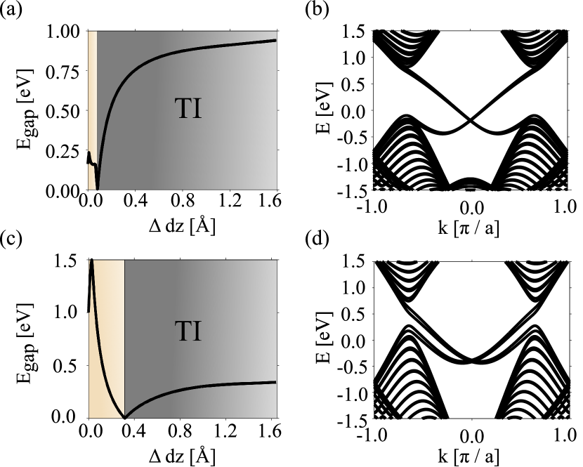
We consider also a transition between bismuth (antimony) bilayer and bismuthene (antimonene) by applying external strain for structures deposited on the substrate. The coupling to the substrate of buckled structure is modeled by shifting the energy of for one atom from a unit cell. The second atom has the energy of orbital eV, as it is fully coupled to the substrate for all strain values. In Fig. 4(a) and (c) we show that bilayers () deposited on a substrate are within a trivial insulator phase. One can see that a very small strain corresponding to for bismuth and for antimony, induces a transition to TI phase with the energy gap monotonically increasing to the largest value for flat systems, bismuthene and antimonene, the right limits of in Fig. 4(a) and (c) respectively. In Fig. 4(b) and (d) we show corresponding band structures of systems in a ribbon geometry for Å. A pair of edge states crosses the energy gap, as is expected for TI phase. The degeneracy of these edge states is removed due to inversion-symmetry breaking - two atoms from a unit cell are inequivalent for a buckled structure as they coupled with different strength to the substrate.
5 Entanglement spectra of Bi and Sb zigzag nanoribbons
Topological properties of the system can be confirmed by analyzing the structure of the entanglement spectrum. The presence of spectral flow in ES is associated with nontrivial band topology of the system. The number of intersecting branches of edge states in the band structure of a system in a ribbon geometry allows one to distinguish between TI and TCI phases, compare Fig. 4(b) and (d) (TI) with Fig. 6(a) and (c) (TCI). Similar features can be also observed in entanglement spectra.
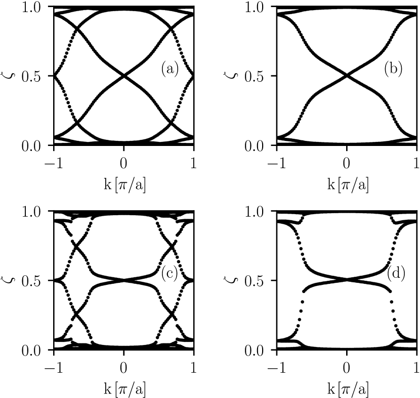
In Fig. 5, we present the single-particle ES for (a) bismuthene and (c) antimonene in a vacuum, together with results for (b) Bi and (d) Sb bilayers on a substrate. Two pairs of intersecting branches are exhibited in TCI phase. It is in analogy to the edge modes in the band structures from Ref. [8] and Fig. 6 in Section 6. In Figs 5 (b) and (d), only one pair of modes spectrally connecting ’s and ’s is noticed and we identify these spectra with TI phase.
6 Transport properties
We focus on the topological protection of transport through edge states in zigzag-type nanoribbons of bismuthene and antimonene in a vacuum, corresponding to systems within TCI phase. In both, bismuthene in Fig. 6(a) and antimonene in Fig. 6(c), we observe four branches of in-gap edge states with edge localization denoted by a size of blue circles. The edge states extend deeply into nanoribbon conduction band, which is novel with respect to previously studied Bi and Sb nanoribbons in TI region [31]. Transport in the clean samples with the Fermi energy in the energy gap shows expected conductance equal to for bismuthene. Antimonene edge states have nonlinear dispersion and eight edge states cross the Fermi level at some energies, e.g. around the Fermi energy eV, 6(c).
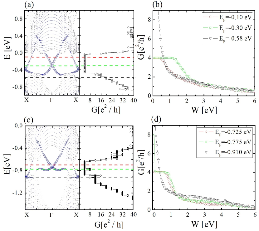
Fig. 6 (b) and (d) present results of transport calculations in the disorder samples for three different Fermi energies in both bismuthene and antimonene. For eV in bismuthene in Fig. 6(b) one can observe protection against backscattering up to the disorder strength eV. This critical value of increases with the lowering of the Fermi energy to eV and can be explained by a larger energetic distance to scattering channels from the conduction band states and a higher level of localization at the edges of the system, larger blue circles in Fig 6(a). A critical disorder strength is smaller in a case of antimonene, which can be related to nonlinear dispersion of edge states and possible scattering within edge channels and also the smaller energy gap in comparison to bismuthene. Analogously to TI nanoribbons, we do not observe any protection against scattering for transport with Fermi energies within both conduction and valence bands, e.g. the latter case represented by eV in Fig. 6(a) and eV in Fig. 6(c). However, within the energy gap region, while Anderson type of disorder breaks a crystal symmetry, robust conductance is still expected.
7 Summary and discussion
In summary, we have studied topological phases in Bi and Sb planar and buckled honeycomb crystals using multi-orbital TB method and compared the results with our and previous DFT calculations. We have shown that TB method correctly predicts topological phases in these systems. Weak coupling to the substrate of buckled and planar crystals is sufficient to lead to a transition to topological insulator phase. We have also proved that entanglement spectra can distinguish between TCI and TI phases which is revealed by two and one pair of branches of entanglement energies in a spectral flow, respectively. We have analyzed also TCI phase in the context of topological protection against scattering during transport through edge channels. Robust quantized conductance is observed even in a presence of a symmetry breaking Anderson disorder.
8 acknowledgments
The authors acknowledge partial financial support from National Science Center (NCN), Poland, grant Maestro No. 2014/14/A/ST3/00654. Our calculations were performed in the Wrocław Center for Networking and Supercomputing.
References
- [1] M. Z. Hasan, C. L. Kane, Colloquium: topological insulators, Reviews of Modern Physics 82 (4) (2010) 3045.
- [2] X.-L. Qi, S.-C. Zhang, Topological insulators and superconductors, Reviews of Modern Physics 83 (4) (2011) 1057.
- [3] L. Fu, C. L. Kane, Topological insulators with inversion symmetry, Physical Review B 76 (4) (2007) 045302.
- [4] Y. Ando, Topological insulator materials, Journal of the Physical Society of Japan 82 (10) (2013) 102001.
- [5] J. E. Moore, The birth of topological insulators, Nature 464 (7286) (2010) 194–198.
- [6] L. Fu, Topological crystalline insulators, Physical Review Letters 106 (10) (2011) 106802.
- [7] T. H. Hsieh, H. Lin, J. Liu, W. Duan, A. Bansil, L. Fu, Topological crystalline insulators in the snte material class, Nature Communications 3 (2012) 982.
- [8] C.-H. Hsu, Z.-Q. Huang, C. P. Crisostomo, L.-Z. Yao, F.-C. Chuang, Y.-T. Liu, B. Wang, C.-H. Hsu, C.-C. Lee, H. Lin, et al., Two-dimensional topological crystalline insulator phase in sb/bi planar honeycomb with tunable dirac gap, Scientific Reports 6 (2016) srep18993.
- [9] S. Safaei, M. Galicka, P. Kacman, R. Buczko, Quantum spin hall effect in iv-vi topological crystalline insulators, New Journal of Physics 17 (6) (2015) 063041.
- [10] J. Zhou, P. Jena, Two-dimensional topological crystalline quantum spin hall effect in transition metal intercalated compounds, Physical Review B 95 (8) (2017) 081102.
- [11] L.-Z. Yao, C. P. Crisostomo, C.-C. Yeh, S.-M. Lai, Z.-Q. Huang, C.-H. Hsu, F.-C. Chuang, H. Lin, A. Bansil, Predicted growth of two-dimensional topological insulator thin films of iii-v compounds on si (111) substrate, Scientific Reports 5.
- [12] B. A. Bernevig, S.-C. Zhang, Quantum spin hall effect, Physical Review Letters 96 (10) (2006) 106802.
- [13] C. L. Kane, E. J. Mele, Z 2 topological order and the quantum spin hall effect, Physical Review Letters 95 (14) (2005) 146802.
- [14] C. L. Kane, E. J. Mele, Quantum spin hall effect in graphene, Physical Review Letters 95 (22) (2005) 226801.
- [15] C.-C. Liu, W. Feng, Y. Yao, Quantum spin hall effect in silicene and two-dimensional germanium, Physical Review Letters 107 (7) (2011) 076802.
- [16] M. König, S. Wiedmann, C. Brüne, A. Roth, H. Buhmann, L. W. Molenkamp, X.-L. Qi, S.-C. Zhang, Quantum spin hall insulator state in hgte quantum wells, Science 318 (5851) (2007) 766–770.
- [17] C. Liu, T. L. Hughes, X.-L. Qi, K. Wang, S.-C. Zhang, Quantum spin hall effect in inverted type-ii semiconductors, Physical Review Letters 100 (23) (2008) 236601.
- [18] I. Knez, R.-R. Du, G. Sullivan, Evidence for helical edge modes in inverted inas/gasb quantum wells, Physical Review Letters 107 (13) (2011) 136603.
- [19] F.-C. Chuang, L.-Z. Yao, Z.-Q. Huang, Y.-T. Liu, C.-H. Hsu, T. Das, H. Lin, A. Bansil, Prediction of large-gap two-dimensional topological insulators consisting of bilayers of group iii elements with bi, Nano Letters 14 (5) (2014) 2505–2508.
- [20] C. P. Crisostomo, L.-Z. Yao, Z.-Q. Huang, C.-H. Hsu, F.-C. Chuang, H. Lin, M. A. Albao, A. Bansil, Robust large gap two-dimensional topological insulators in hydrogenated iii–v buckled honeycombs, Nano Letters 15 (10) (2015) 6568–6574.
- [21] L. Li, X. Zhang, X. Chen, M. Zhao, Giant topological nontrivial band gaps in chloridized gallium bismuthide, Nano Letters 15 (2) (2015) 1296–1301.
- [22] M. Zhao, X. Chen, L. Li, X. Zhang, Driving a gaas film to a large-gap topological insulator by tensile strain, Scientific Reports 5.
- [23] S. Murakami, Quantum spin hall effect and enhanced magnetic response by spin-orbit coupling, Physical Review Letters 97 (23) (2006) 236805.
- [24] M. Wada, S. Murakami, F. Freimuth, G. Bihlmayer, Localized edge states in two-dimensional topological insulators: Ultrathin bi films, Physical Review B 83 (12) (2011) 121310.
-
[25]
P. F. Zhang, Z. Liu, W. Duan, F. Liu, J. Wu,
Topological and
electronic transitions in a sb(111) nanofilm: The interplay between quantum
confinement and surface effect, Phys. Rev. B 85 (2012) 201410.
doi:10.1103/PhysRevB.85.201410.
URL https://link.aps.org/doi/10.1103/PhysRevB.85.201410 - [26] Z.-Q. Huang, C.-H. Hsu, F.-C. Chuang, Y.-T. Liu, H. Lin, W.-S. Su, V. Ozolins, A. Bansil, Strain driven topological phase transitions in atomically thin films of group iv and v elements in the honeycomb structures, New Journal of Physics 16 (10) (2014) 105018.
- [27] I. K. Drozdov, A. Alexandradinata, S. Jeon, S. Nadj-Perge, H. Ji, R. Cava, B. A. Bernevig, A. Yazdani, One-dimensional topological edge states of bismuth bilayers, Nature Physics 10 (9) (2014) 664–669.
- [28] N. Kawakami, C.-L. Lin, M. Kawai, R. Arafune, N. Takagi, One-dimensional edge state of bi thin film grown on si (111), Applied Physics Letters 107 (3) (2015) 031602.
- [29] F. Yang, L. Miao, Z. Wang, M.-Y. Yao, F. Zhu, Y. Song, M.-X. Wang, J.-P. Xu, A. V. Fedorov, Z. Sun, et al., Spatial and energy distribution of topological edge states in single bi (111) bilayer, Physical Review Letters 109 (1) (2012) 016801.
- [30] F. Reis, G. Li, L. Dudy, M. Bauernfeind, S. Glass, W. Hanke, R. Thomale, J. Schäfer, R. Claessen, Bismuthene on a sic substrate: A candidate for a high-temperature quantum spin hall material, Science 357 (6348) (2017) 287–290.
- [31] M. Bieniek, T. Woźniak, P. Potasz, Stability of topological properties of bismuth (1 1 1) bilayer, Journal of Physics: Condensed Matter 29 (15) (2017) 155501.
-
[32]
X. Li, H. Liu, H. Jiang, F. Wang, J. Feng,
Edge engineering
of a topological bi(111) bilayer, Phys. Rev. B 90 (2014) 165412.
doi:10.1103/PhysRevB.90.165412.
URL https://link.aps.org/doi/10.1103/PhysRevB.90.165412 -
[33]
Y. M. Koroteev, G. Bihlmayer, E. V. Chulkov, S. Blügel,
First-principles
investigation of structural and electronic properties of ultrathin bi films,
Phys. Rev. B 77 (2008) 045428.
doi:10.1103/PhysRevB.77.045428.
URL https://link.aps.org/doi/10.1103/PhysRevB.77.045428 - [34] H. Pan, X.-S. Wang, Realization of dirac cones in few bilayer sb (111) films by surface modification, Nanoscale Research Letters 10 (1) (2015) 334.
- [35] G. Bian, Z. Wang, X.-X. Wang, C. Xu, S. Xu, T. Miller, M. Z. Hasan, F. Liu, T.-C. Chiang, Engineering electronic structure of a two-dimensional topological insulator bi (111) bilayer on sb nanofilms by quantum confinement effect, ACS Nano 10 (3) (2016) 3859–3864.
- [36] G. Cantele, D. Ninno, Size-dependent structural and electronic properties of bi (111) ultrathin nanofilms from first principles, Physical Review Materials 1 (1) (2017) 014002.
-
[37]
R. R. Q. Freitas, R. Rivelino, F. de Brito Mota, C. M. C. de Castilho,
A. Kakanakova-Georgieva, G. K. Gueorguiev,
Topological insulating
phases in two-dimensional bismuth-containing single layers preserved by
hydrogenation, The Journal of Physical Chemistry C 119 (41) (2015)
23599–23606.
arXiv:http://dx.doi.org/10.1021/acs.jpcc.5b07961, doi:10.1021/acs.jpcc.5b07961.
URL http://dx.doi.org/10.1021/acs.jpcc.5b07961 - [38] M. Bieniek, T. Woźniak, P. Potasz, Study of spin-orbit coupling effect on bismuth (111) bilayer, Acta Physica Polonica A 130 (2) (2016) 609–612.
- [39] K.-H. Jin, S.-H. Jhi, Quantum anomalous hall and quantum spin-hall phases in flattened bi and sb bilayers, Scientific Reports 5.
- [40] F.-C. Chuang, C.-H. Hsu, C.-Y. Chen, Z.-Q. Huang, V. Ozolins, H. Lin, A. Bansil, Tunable topological electronic structures in sb (111) bilayers: A first-principles study, Applied Physics Letters 102 (2) (2013) 022424.
- [41] Z.-Q. Huang, F.-C. Chuang, C.-H. Hsu, Y.-T. Liu, H.-R. Chang, H. Lin, A. Bansil, Phys. Rev. B 88 (2013) 165301.
- [42] Z.-Q. Huang, F.-C. Chuang, C.-H. Hsu, Y.-T. Liu, H.-R. Chang, H. Lin, A. Bansil, Nontrivial topological electronic structures in a single bi (111) bilayer on different substrates: A first-principles study, Physical Review B 88 (16) (2013) 165301.
- [43] C.-H. Hsu, Z.-Q. Huang, F.-C. Chuang, C.-C. Kuo, Y.-T. Liu, H. Lin, A. Bansil, The nontrivial electronic structure of bi/sb honeycombs on sic (0001), New Journal of Physics 17 (2) (2015) 025005.
- [44] C.-C. Liu, S. Guan, Z. Song, S. A. Yang, J. Yang, Y. Yao, Low-energy effective hamiltonian for giant-gap quantum spin hall insulators in honeycomb x-hydride/halide (x= n–bi) monolayers, Physical Review B 90 (8) (2014) 085431.
- [45] T. Hirahara, N. Fukui, T. Shirasawa, M. Yamada, M. Aitani, H. Miyazaki, M. Matsunami, S. Kimura, T. Takahashi, S. Hasegawa, K. Kobayashi, Phys. Rev. Lett. 109 (2012) 227401.
- [46] Z. Liu, C.-X. Liu, Y.-S. Wu, W.-H. Duan, F. Liu, J. Wu, Phys. Rev. Lett. 107 (2011) 136805.
- [47] Y. Liu, R. E. Allen, Phys. Rev. B 52 (1995) 1566.
- [48] S. Murakami, Phys. Rev. 94 (1954) 1498.
- [49] D. Chadi, Spin-orbit splitting in crystalline and compositionally disordered semiconductors, Physical Review B 16 (2) (1977) 790.
- [50] Z. Liu, C.-X. Liu, Y.-S. Wu, W.-H. Duan, F. Liu, J. Wu, Stable nontrivial z 2 topology in ultrathin bi (111) films: a first-principles study, Physical Review Letters 107 (13) (2011) 136805.
- [51] Y. Liu, R. E. Allen, Electronic structure of the semimetals bi and sb, Physical Review B 52 (3) (1995) 1566.
- [52] J. P. Perdew, K. Burke, M. Ernzerhof, Generalized gradient approximation made simple, Physical Review Letters 77 (18) (1996) 3865.
- [53] H. J. Monkhorst, J. D. Pack, Special points for brillouin-zone integrations, Physical Review B 13 (12) (1976) 5188.
-
[54]
P. Giannozzi, S. Baroni, N. Bonini, M. Calandra, R. Car, C. Cavazzoni,
D. Ceresoli, G. L. Chiarotti, M. Cococcioni, I. Dabo, A. D. Corso,
S. de Gironcoli, S. Fabris, G. Fratesi, R. Gebauer, U. Gerstmann,
C. Gougoussis, A. Kokalj, M. Lazzeri, L. Martin-Samos, N. Marzari, F. Mauri,
R. Mazzarello, S. Paolini, A. Pasquarello, L. Paulatto, C. Sbraccia,
S. Scandolo, G. Sclauzero, A. P. Seitsonen, A. Smogunov, P. Umari, R. M.
Wentzcovitch, Quantum
espresso: a modular and open-source software project for quantum simulations
of materials, Journal of Physics: Condensed Matter 21 (39) (2009) 395502.
URL http://stacks.iop.org/0953-8984/21/i=39/a=395502 - [55] O. Ü. Aktürk, V. O. Özçelik, S. Ciraci, Single-layer crystalline phases of antimony: Antimonenes, Physical Review B 91 (23) (2015) 235446.
- [56] E. Aktürk, O. Ü. Aktürk, S. Ciraci, Single and bilayer bismuthene: Stability at high temperature and mechanical and electronic properties, Physical Review B 94 (1) (2016) 014115.
- [57] I. Peschel, Calculation of reduced density matrices from correlation functions, Journal of Physics A: Mathematical and General 36 (14) (2003) L205.
-
[58]
T. L. Hughes, E. Prodan, B. A. Bernevig,
Inversion-symmetric
topological insulators, Phys. Rev. B 83 (2011) 245132.
doi:10.1103/PhysRevB.83.245132.
URL https://link.aps.org/doi/10.1103/PhysRevB.83.245132 -
[59]
A. M. Turner, Y. Zhang, A. Vishwanath,
Entanglement and
inversion symmetry in topological insulators, Phys. Rev. B 82 (2010) 241102.
doi:10.1103/PhysRevB.82.241102.
URL https://link.aps.org/doi/10.1103/PhysRevB.82.241102 - [60] D. Wang, L. Chen, H. Liu, X. Wang, Electronic structures and topological properties of bi (111) ultrathin films, Journal of the Physical Society of Japan 82 (9) (2013) 094712.