Measurement of a Magnonic Crystal at Millikelvin Temperatures
Abstract
Hybrid systems combining magnons and superconducting quantum circuits have attracted increasing interest in recent years. Magnonic crystals (MCs) are one of the building blocks of room-temperature magnonics and can be used to create devices with an engineered band structure. These devices, exhibiting tunable frequency selectivity and the ability to store travelling excitations in the microwave regime, may form the basis of a set of tools to be used in the context of quantum information processing. In order to ascertain the feasibility of such plans, MCs must be demonstrated to work at the low temperatures required for microwave-frequency quantum experiments. We report the measurements of the transmission of microwave signals through an MC at mK and observe a magnonic bandgap in both continuous-wave and pulsed excitation experiments. The spin-wave damping at low temperatures in our yttrium iron garnet MC is higher than expected, indicating that further work is necessary before the full potential of quantum experiments using magnonic crystals can be realised.
pacs:
Superconducting quantum circuits have become an increasingly mature experimental technology in recent years Devoret et al. (2004); Gambetta et al. (2017). As a result, there has been a surge of interest within the circuit quantum electrodynamics (circuit QED) community in combining such circuits with other physical systems such as spin ensembles Kurizki et al. (2015); You and Nori (2011), acoustic waves Gustafsson et al. (2014), and magnonic structures Tabuchi et al. (2016).
The goal of quantum magnonics is to investigate the physics of magnons at the quantum level and to create novel microwave devices useful for quantum information processing. Dipolar magnons (spin waves) Kruglyak et al. (2010) have m-wavelengths and are readily excited over a range of microwave frequencies which overlap with those of superconducting quantum circuits. Recent work includes the measurement of surface spin waves in a m-thick yttrium iron garnet (YIG) waveguide at millikelvin temperatures van Loo et al. (2016), the demonstration of strong coupling between bulk YIG samples and resonators Huebl et al. (2012); Tabuchi et al. (2014); Goryachev et al. (2014); Zhang et al. (2015); Bourhill et al. (2015); Kostylev et al. (2016); Morris et al. (2017) and the excitation of a single magnon in a YIG sphere using a superconducting qubit Tabuchi et al. (2015); Lachance-Quirion et al. (2017).
Magnonic crystals (MCs) Krawczyk and Grundler (2014); Chumak et al. (2017), the magnetic analogue of photonic crystals, are magnetic waveguides with artificially engineered magnonic bandgaps. MCs are created by imposing periodic changes in a waveguide’s magnetic properties or environment. Various implementations have been demonstrated, including several static varieties and a dynamic variant with a bandgap that can be switched on and off.
At room temperature, MCs have been used to create a range of devices including oscillators and filters Karenowska et al. (2010), logic gates Nikitin et al. (2015), and magnon transistors Chumak et al. (2014). Several of the properties of magnonic crystals — notably their strong and tunable frequency selectivity, storage capability, and ability to alter the propagation direction of signals — have potential utility in the manipulation of single magnon excitations in experimental solid-state quantum devices Chumak et al. (2010, 2012). Until now, however, it remained to be established that MCs can be used at the millikelvin temperatures required for such devices. In this work, we present measurements of a magnonic crystal at millikelvin temperatures, a step towards the incorporation of MCs into quantum devices.
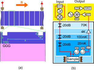
The basis for the magnonic crystal used in our experiments is a structured YIG waveguide (thickness m, room-temperature saturation magnetization kA/m) epitaxially grown on a gadolinium gallium garnet (GGG) substrate. YIG, a ferrimagnetic electrical insulator, has extremely low spin-wave damping at room temperature and is therefore much used in room-temperature magnonic device development Serga et al. (2010). The MC is formed from a series of eight equally-spaced grooves, each of width m and depth m, chemically etched into the magnetic film. The distance between the grooves is m (see fig. 1(a)). Spin waves are excited and detected by niobium microstrip antennae fabricated mm apart on a sapphire crystal substrate in direct contact with the MC. In order to assure compatibility with the thin-film superconducting measurement structures used in circuit QED, it is desirable to apply the required bias magnetic field in-plane. We chose to carry out our experiments in the backward volume geometry (BVMSW) Hurben and Patton (1995) (bias magnetic field parallel to the spin-wave propagation direction (), which is along the longitudinal axis of the waveguide). At room temperature, crystals measured in the backward volume configuration have been shown to display bandgaps with a higher rejection ratio than magnetostatic surface spin waves (MSSW) (, in-plane field) Chumak et al. (2009).
A dilution refrigerator is used to cool the MC assembly, housed in a copper sample box, down to mK. Figure 1(b) shows a schematic of the measurement setup. A superconducting coil provides the static magnetic field necessary to bias the magnetic sample. A microwave source, IQ-mixer and arbitrary waveform generator (AWG) are used to create microwave input pulses. Three dB attenuators in the input line ensure that the electrical noise temperature of the input signals is comparable to the thermodynamic temperature of the sample. Output signals pass through two -terminated circulators before being amplified at the K stage. Outside the fridge, the output signals are down-converted to 500 MHz. A fast data acquisition (DAQ) card digitises the down-converted signal at a sampling frequency of 2.5 GHz. Signals are typically averaged 20,000 times on the DAQ card before being digitally demodulated.
The MC is first characterised at room temperature using a network analyser. Figure 2 shows the transmission measured at room temperature as a function of microwave input signal frequency with mT. The displayed data is relative to that measured at zero field, i.e. when no spin waves are excited within the waveguide and only directly-coupled electromagnetic signals propagate between the input and output antennae through the vacuum of the sample box. In this figure, the highest frequency at which the BVMSW are observed corresponds to the spins precessing uniformly throughout the material (FMR, ). Propagating modes () have lower frequencies. The low-frequency (high-) limit of the measurable band is determined by the geometry of the microwave antennae. High- excitations couple less well than low- ones to these structures, the coupling becoming negligible once the wavelength is smaller than the antenna width.
Below the FMR frequency, the data displays oscillations caused by the interference between the spin-wave signal and the directly-coupled signal; due to the different dispersion relation of the magnonic and photonic waves, these signals accumulate different phases while travelling to the output antenna, resulting in interference fringes. The magnonic bandgaps of the crystal appear as gaps in this pattern: in the bandgaps, the transmitted spin-wave signal is suppressed while the directly-coupled signal is unaffected, resulting in regions without oscillations.
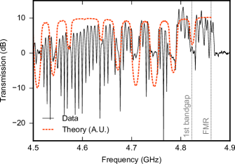
Calculations were made using the transfer matrix method following the treatment of Chumak Chumak et al. (2009). In this model, spin waves accumulate phase and experience damping while propagating in between neighbouring edges of the grooves defining the lattice of the magnonic crystal. At the interfaces between etched and unetched regions, spin waves undergo partial reflection and transmission. For completeness, it should be noted that the coupling of the antennae to the waveguide has some dependence on which is not included in the model: the effect of this on the key qualitative features being fitted (namely the position and width of the bandgaps) is negligible.
Apart from the FMR linewidth (), two phenomenological parameters appear in the model: which accounts for the increased damping due to two-magnon scattering within the grooves, and which is used to match the predicted and observed width and depth of the bandgaps. For simplicity, in our calculations is set to zero and is adjusted to fit the measured widths of the gaps. The theoretical prediction of the transmission characteristics across the magnonic crystal with kA/m (dotted line in fig. 2) is consistent with the observed positions and widths of the bandgaps.
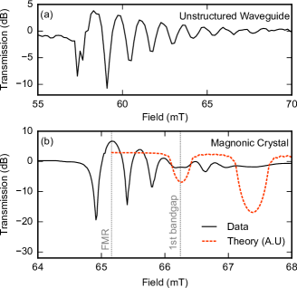
Figure 3 compares the transmission characteristics of an unstructured magnonic waveguide (m film thickness, mm inter-antennae spacing) and the same magnonic crystal at 20 mK. An offset has been applied to the data to shift the baseline to dB. In contrast to the room-temperature measurement in fig. 2, measurements at mK are made as a function of the magnetic bias field () while keeping the input frequency constant. The system is excited using a constant frequency 4 GHz microwave tone with a power of dBm at the input of the antenna. The lowest field at which the BVMSWs are observed corresponds to the FMR. Signals at higher fields are propagating modes ().
At mK, the measurement of the unstructured waveguide (fig. 3(a)) shows oscillations across the spin-wave passband that decay in amplitude as increases (i.e. as increases). As in the data of fig. 2, the oscillations are due to the interference between the spin-wave and directly-coupled signals. As anticipated, without the etched grooves, no magnonic bandgap is present. In the MC measurement (fig. 3(b)), a single bandgap is observed. Its position at 66.2 mT agrees with that predicted using the transfer matrix method with a saturation magnetisation of kA/m van Loo et al. (2016); Maier-Flaig et al. (2017). Note that in the transfer matrix model, neither the position nor the width of the bandgaps are significantly affected by changing the parameter . Accordingly, when we calculate where the bandgaps are expected at low temperature, we use the room-temperature value of this parameter with the proviso that this modelling is not intended to reveal the additional low-temperature damping: it is solely a tool for identifying the position and width of the gaps.
The range of -values over which spin-wave signals are measurable is found to be substantially narrower at low temperature than it was at room temperature ( rad/cm at mK versus rad/cm at room temperature), indicating a higher damping constant. The effect of higher damping on the measured signal is more severe at higher (higher field in fig. 3, lower frequency in fig. 2) owing to the shape of the BVMSW dispersion curve: since the magnitude of the spin-wave group velocity decreases with increasing wavenumber, excitations with higher take longer to traverse the waveguide and are therefore more severely damped Chumak et al. (2009). In our mK experiments, the spin-wave signal at the -value corresponding to the second bandgap is too weak to be detected.
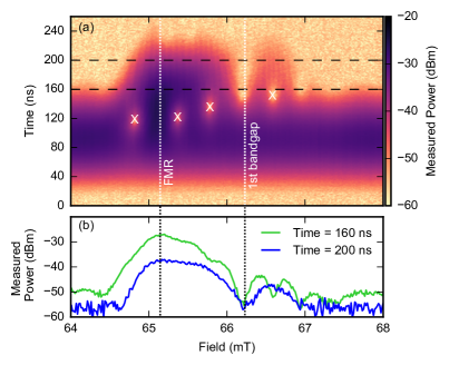
The presence of a magnonic bandgap can also be observed in time-resolved measurements at 20 mK. Since the spin waves propagate slower than the directly-coupled signal (which travels at the speed of light to the output antenna), for sufficiently short excitation pulses, the two can be separated in time. Care has to be taken, however, not to make pulses so short as to have a frequency bandwidth that exceeds the width of the bandgap: under these conditions the gap cannot be observed since the signal always has a component lying outside of the bandgap which can propagate freely through the crystal.
Figure 4 shows the time response of the magnonic crystal to a Gaussian pulse (ns) with a carrier frequency of GHz. Such pulses are slightly too long to allow complete temporal separation between the directly-coupled signal and the spin-wave signal, but the bandgap starts to be obscured if they are made shorter. Initially, only the directly-coupled signal is measured ( ns ns). When the spin waves start to arrive at the output antenna ( ns ns), they overlap in time with the directly-coupled signals, interfering destructively at ‘X’ in fig. 4. Beyond 160 ns, the directly-coupled signal disappears, leaving only the transmitted spin-wave signal. Figure 4(b) shows the linecuts from the same data at ns and ns. The first bandgap of the magnonic crystal is visible at mT, consistent with the continuous-wave measurement in fig. 3(b).
A comparison between the room-temperature (fig. 2) and cold data (fig. 3(b)) indicates the presence of a significant increase in spin-wave damping at millikelvin temperatures. There are three possible sources of damping that warrant careful consideration: magnetic impurities in the YIG, enhanced damping due to the scattering processes caused by uneven etching of the grooves, and the GGG substrate upon which the MC is grown.
Previous measurements Spencer et al. (1959); Maier-Flaig et al. (2017); Haidar et al. (2015); Jermain et al. (2017) have shown that FMR linewidths in YIG initially increase as the material’s temperature is decreased (below K), reach a maximum value, and then begin to reduce again. This is generally attributed to the presence of paramagnetic rare-earth impurities in YIG with temperature-dependent relaxation times. While the lowest temperatures reached in these earlier works are around K, they consistently report decreasing linewidths when the temperature is reduced below K. Furthermore, the linewidths of YIG spheres measured in Refs. Tabuchi et al. (2014) and Zhang et al. (2015) at millikelvin temperatures are similar to the values observed at room temperature. From this, it seems likely that it is feasible to produce a pure YIG material with a linewidth at millikelvin temperatures comparable to the room-temperature value.
The surface roughness of a ferrite sample is known to influence the FMR linewidth because it increases two-magnon scattering, especially in a thin film sample Gurevich and Melkov (1996). Spencer Spencer et al. (1959) has shown that better polished YIG spheres do exhibit lower linewidths across a range of temperature, from K down to K. Rough surfaces inside the grooves which define an etched MC are known to contribute to damping Chumak et al. (2009) but, as yet, there is no reason to think that this effect would be significantly enhanced at low temperatures.
The substrate upon which the YIG film is grown, gadolinium gallium garnet, is known to be paramagnetic below K Danilov et al. (1989). GGG is well-known to have a frustrated spin system with an ordered antiferromagnetic state below mK at a relatively high field (T) Schiffer et al. (1994). At low field, the material undergoes a spin glass transition below mK Schiffer et al. (1995). While its behaviour at the intermediate field ranges of our experiments is not well-documented, given these known magnetic properties and the relatively narrow linewidths measured in bulk YIG at low temperature (i.e. in the absence of GGG) it seems highly likely that, if not the only culprit, losses due to its low-temperature magnetic system coupling to the YIG are at least an important contributor to the increased damping we observe.
In conclusion, we have measured a bandgap in a magnonic crystal consisting of an etched YIG waveguide at mK. Our results are consistent with calculations based on the transfer matrix method, both for continuous-wave and time-resolved measurements. Room-temperature and cold measurements of the same magnonic crystal indicate the presence of higher-than-expected spin-wave damping in the YIG at millikelvin temperatures. Future experiments investigating spin waves in YIG waveguides at millikelvin temperatures may provide more insight into the nature of this damping. This is essential if magnonic crystals are to be used for manipulation of magnons at the quantum level.
Acknowledgements.
This work was supported by the Engineering and Physical Sciences Research Council grant EP/K032690/1. We acknowledge A.V. Chumak for the magnonic crystal sample and J.F. Gregg for the use of his room-temperature magnet. S. Kosen acknowledges the Indonesia Endowment Fund for Education.References
- Devoret et al. (2004) M. H. Devoret, A. Wallraff, and J. M. Martinis, (2004), arXiv:0411174 [cond-mat] .
- Gambetta et al. (2017) J. M. Gambetta, J. M. Chow, and M. Steffen, npj Quantum Information 3, 2 (2017), arXiv:1510.04375 .
- Kurizki et al. (2015) G. Kurizki, P. Bertet, Y. Kubo, K. Mølmer, D. Petrosyan, P. Rabl, and J. Schmiedmayer, Proceedings of the National Academy of Sciences 112, 3866 (2015), arXiv:1504.00158 .
- You and Nori (2011) J. Q. You and F. Nori, Nature 474, 589 (2011), arXiv:1202.1923 .
- Gustafsson et al. (2014) M. V. Gustafsson, T. Aref, A. F. Kockum, M. K. Ekstrom, G. Johansson, and P. Delsing, Science 346, 207 (2014), arXiv:1404.0401 .
- Tabuchi et al. (2016) Y. Tabuchi, S. Ishino, A. Noguchi, T. Ishikawa, R. Yamazaki, K. Usami, and Y. Nakamura, Comptes Rendus Physique 17, 729 (2016), arXiv:1508.05290 .
- Kruglyak et al. (2010) V. V. Kruglyak, S. O. Demokritov, and D. Grundler, Journal of Physics D: Applied Physics 43, 264001 (2010).
- van Loo et al. (2016) A. F. van Loo, R. G. E. Morris, and A. D. Karenowska, (2016), arXiv:1610.08402 .
- Huebl et al. (2012) H. Huebl, C. Zollitsch, J. Lotze, F. Hocke, M. Greifenstein, A. Marx, R. Gross, and S. T. B. Goennenwein, Physical Review Letters 111, 1 (2012), arXiv:1207.6039 .
- Tabuchi et al. (2014) Y. Tabuchi, S. Ishino, T. Ishikawa, R. Yamazaki, K. Usami, and Y. Nakamura, Physical Review Letters 113, 1 (2014), arXiv:1405.1913 .
- Goryachev et al. (2014) M. Goryachev, W. G. Farr, D. L. Creedon, Y. Fan, M. Kostylev, and M. E. Tobar, Phys. Rev. Applied 2, 54002 (2014), arXiv:1408.2905 .
- Zhang et al. (2015) D. Zhang, X.-m. Wang, T.-f. Li, X.-q. Luo, W. Wu, F. Nori, and J. You, npj Quantum Information 1 (2015), 10.1038/npjqi.2015.14, arXiv:1512.00983 .
- Bourhill et al. (2015) J. Bourhill, N. Kostylev, M. Goryachev, D. Creedon, and M. Tobar, Phys. Rev. B 93, 144420 (2015), arXiv:1512.07773 .
- Kostylev et al. (2016) N. Kostylev, M. Goryachev, and M. E. Tobar, Applied Physics Letters 108 (2016), 10.1063/1.4941730, arXiv:1508.04967 .
- Morris et al. (2017) R. G. E. Morris, A. F. van Loo, S. Kosen, and A. D. Karenowska, Scientific Reports 7, 1 (2017), arXiv:1610.09963 .
- Tabuchi et al. (2015) Y. Tabuchi, S. Ishino, A. Noguchi, T. Ishikawa, R. Yamazaki, K. Usami, and Y. Nakamura, Science 349, 405 (2015), arXiv:1410.3781 .
- Lachance-Quirion et al. (2017) D. Lachance-Quirion, Y. Tabuchi, S. Ishino, A. Noguchi, T. Ishikawa, R. Yamazaki, and Y. Nakamura, Science Advances 3 (2017), 10.1126/sciadv.1603150, arXiv:1610.00839 .
- Krawczyk and Grundler (2014) M. Krawczyk and D. Grundler, Journal of Physics: Condensed Matter 26, 123202 (2014).
- Chumak et al. (2017) A. V. Chumak, A. A. Serga, and B. Hillebrands, Journal of Physics D: Applied Physics 50, 1 (2017), arXiv:1702.06701 .
- Karenowska et al. (2010) A. D. Karenowska, A. V. Chumak, A. A. Serga, J. F. Gregg, and B. Hillebrands, Applied Physics Letters 96, 2008 (2010), arXiv:0912.2029 .
- Nikitin et al. (2015) A. A. Nikitin, A. B. Ustinov, A. A. Semenov, A. V. Chumak, A. A. Serga, V. I. Vasyuchka, E. Lähderanta, B. A. Kalinikos, and B. Hillebrands, Applied Physics Letters 106 (2015), 10.1063/1.4914506, arXiv:1501.03486v2 .
- Chumak et al. (2014) A. V. Chumak, A. A. Serga, and B. Hillebrands, Nature Communications 5, 4700 (2014).
- Chumak et al. (2010) A. V. Chumak, V. S. Tiberkevich, A. D. Karenowska, A. A. Serga, J. F. Gregg, A. N. Slavin, and B. Hillebrands, Nature Communications 1, 141 (2010).
- Chumak et al. (2012) A. V. Chumak, V. I. Vasyuchka, A. A. Serga, M. P. Kostylev, V. S. Tiberkevich, and B. Hillebrands, Phys. Rev. Lett. 108 (2012), 10.1103/physrevlett.108.257207, arXiv:1107.0984 .
- Serga et al. (2010) A. A. Serga, A. V. Chumak, and B. Hillebrands, Journal of Physics D: Applied Physics 43, 264002 (2010).
- Hurben and Patton (1995) M. J. Hurben and C. E. Patton, Journal of Magnetism and Magnetic Materials 139, 263 (1995).
- Chumak et al. (2009) A. V. Chumak, A. A. Serga, S. Wolff, B. Hillebrands, and M. P. Kostylev, Applied Physics Letters 94, 8 (2009), arXiv:0903.3686 .
- Maier-Flaig et al. (2017) H. Maier-Flaig, S. Klingler, C. Dubs, O. Surzhenko, R. Gross, M. Weiler, H. Huebl, and S. T. Goennenwein, Physical Review B 95, 1 (2017), arXiv:1703.09444 .
- Spencer et al. (1959) E. Spencer, R. LeCraw, and A. Clogston, Physical Review Letters 3, 32 (1959).
- Haidar et al. (2015) M. Haidar, M. Ranjbar, M. Balinsky, R. K. Dumas, S. Khartsev, and J. Åkerman, Journal of Applied Physics 117, 115 (2015).
- Jermain et al. (2017) C. L. Jermain, S. V. Aradhya, N. D. Reynolds, R. A. Buhrman, J. T. Brangham, M. R. Page, P. C. Hammel, F. Y. Yang, and D. C. Ralph, Physical Review B 95, 1 (2017), arXiv:1612.01954 .
- Gurevich and Melkov (1996) A. Gurevich and G. Melkov, Magnetization Oscillations and Waves (CRC Press, Inc, 1996).
- Danilov et al. (1989) V. V. Danilov, D. L. Lyfar’, Y. V. Lyubon’ko, A. Y. Nechiporuk, and S. M. Ryabchenko, Soviet Physics Journal 32, 276 (1989).
- Schiffer et al. (1994) P. Schiffer, A. P. Ramirez, D. A. Huse, and A. J. Valentino, Physical Review Letters 73, 2500 (1994).
- Schiffer et al. (1995) P. Schiffer, A. P. Ramirez, D. A. Huse, P. L. Gammel, U. Yaron, D. J. Bishop, and A. J. Valentino, Physical Review Letters 74, 2379 (1995).