Current address: ]Department of Electrical and Computer Engineering, University of Texas at Austin, Austin, TX 78701, USA
Current address: ]Department of Physics, Lawrence University, Appleton, WI 54911, USA
Imaging a Nitrogen-Vacancy Center with a Diamond Immersion Metalens
Solid-state quantum emitters have emerged as robust single-photon sources Aharonovich, Englund, and Toth (2016) and addressable spins Gao et al. (2015) — key components in rapidly developing quantum technologies for broadband magnetometry Rondin et al. (2014), biological sensing Balasubramanian et al. (2014), and quantum information science Awschalom et al. (2013). Performance in these applications, be it magnetometer sensitivity or quantum key generation rate, is limited by the number of photons detected. However, efficient collection of a quantum emitter’s photoluminescence (PL) is challenging as its atomic scale necessitates diffraction-limited imaging with nanometer-precision alignment, oftentimes at cryogenic temperatures. In this letter, we image an individual quantum emitter, an isolated nitrogen-vacancy (NV) center in diamond, using a dielectric metalens composed of subwavelength pillars etched into the diamond’s surface (Fig. 1a). The metalens eliminates the need for an objective by operating as a high-transmission-efficiency immersion lens with a numerical aperture (NA) greater than 1.0. This design provides a scalable approach for fiber coupling solid-state quantum emitters that will enable the development of deployable quantum devices.
Beyond their atomic scale, the challenges associated with coupling to solid-state quantum emitters are exacerbated by the high refractive index of their host substrates. Diamond, for example, has a refractive index of at visible wavelengths, which traps photons emitted above of normal incidence at a planar air interface by total-internal reflection. Furthermore, imaging through more than a few microns of diamond with a high-NA objective results in spherical aberrations that severely limit collection efficiency. While a number of nanophotonic structures have been investigated for increasing NV emission through Purcell enhancementAharonovich and Neu (2014); Lončar and Faraon (2013); Faraon et al. (2013); Schröder et al. (2016), these devices require NVs positioned close to diamond surfaces, which degrades their spinOfori-Okai et al. (2012) and optical propertiesChu et al. (2014). For this reason, the typical approach to addressing single NVs in pristine bulk diamond is to mill or etch a hemispherical surface, known as a solid immersion lens (SIL), centered about an individual NV center. By achieving uniform optical path length and reflectance for rays emanating from the NV at all angles Castelletto et al. (2011), SILs have removed the losses caused by total-internal-reflection and spherical aberration, enabling ground-breaking demonstrations in quantum optics such as the recent loop-hole-free violation of Bell’s inequalityHensen et al. (2015). However, a high-NA objective lens is still required to image a quantum emitter through a SIL. Thus, a cryostat that can accommodate a vacuum-compatible objective and associated optomechanics must be used, or the optical losses associated with imaging through a cryostat window must be accepted. Neither option provides a clear route for packaging quantum emitters in a scalable fashion.
Since quantum emitters are point sources with relatively narrow emission spectra, the compound optical system of a microscope objective, which is designed for broadband imaging with a flat field-of-view, is not strictly necessary for efficient photon collection. A more scalable approach would be to use flat optics, like the phase Fresnel lenses used to image trapped ions in ultra-high vacuum cryostats Jechow et al. (2011). However, a flat optic on its own cannot compensate for the high-refractive index of a solid-state quantum emitter’s host material. The ideal solution would be a flat optic fabricated at the air/diamond interface to form a planar immersion lens; such a design can be realized using the subwavelength elements of a metasurface.
Metasurfaces have recently gained attention as they offer design flexibility for optical components with arbitrary phase responses Kildishev, Boltasseva, and Shalaev (2013); Yu and Capasso (2014). In particular, dielectric metalenses Lalanne and Chavel (2017); Genevet et al. (2017); Khorasaninejad et al. (2016a), diffractive optics Lalanne and Chavel (2017); Lee et al. (2002), and high-contrast gratings Chang-Hasnain and Yang (2012); Vo et al. (2014) comprised of high-refractive-index dielectric elements such as TiO2 and amorphous silicon have been demonstrated with high transmission efficiency and diffraction-limited focusing. While spherical and chromatic aberrations limit the field-of-view of single-element dielectric metalenses as compared to aberration-corrected multi-lens objectives Lalanne and Chavel (2017), they are ideally suited for collimating emission from a point source over a narrow wavelength range.
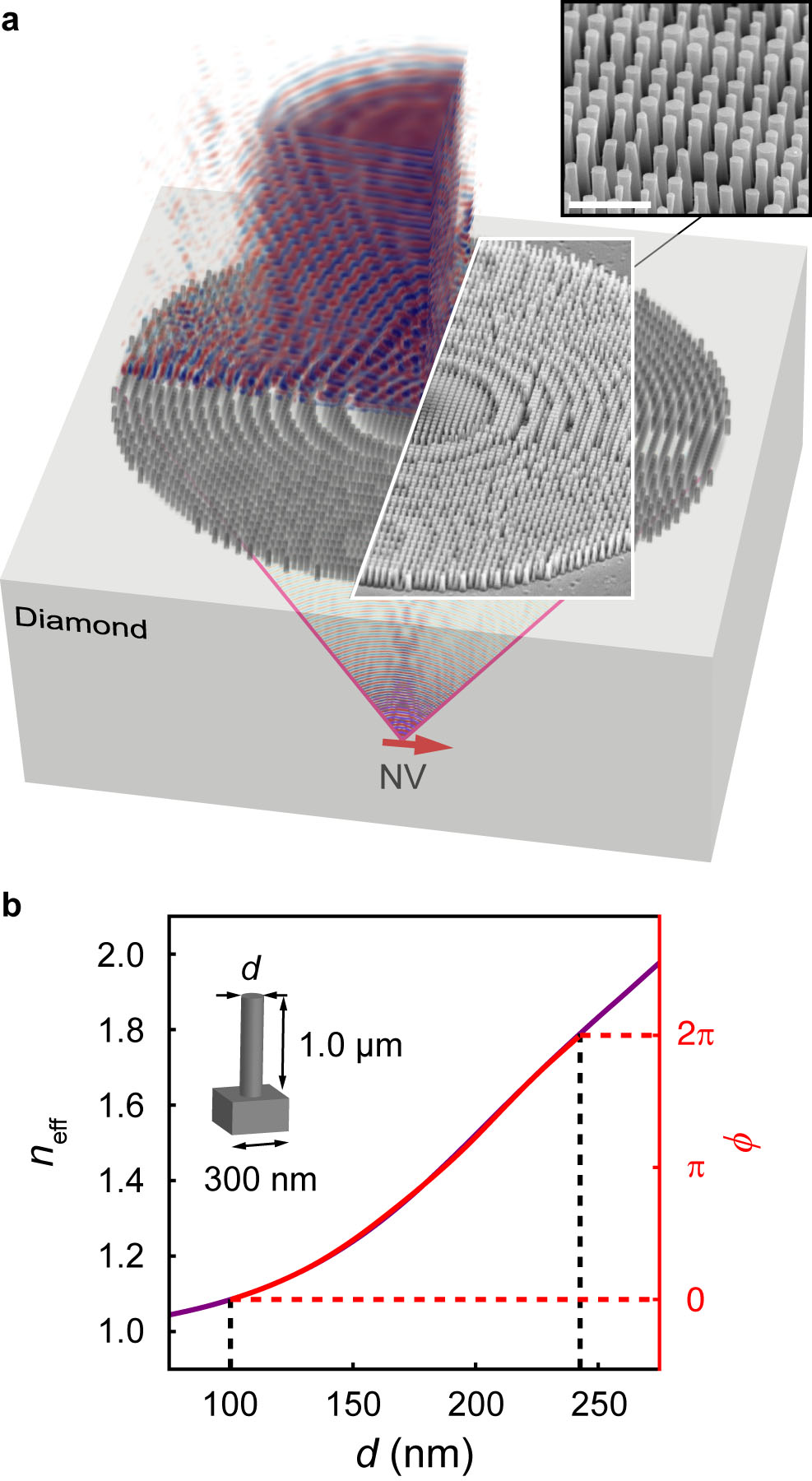
Building on these advances, we leverage diamond’s high refractive index to image an individual NV center located below a -diameter metalens fabricated on the surface of a single-crystal substrate. We demonstrate a transmission efficiency 88% and , and use the metalens to couple NV PL into a fiber with a background-subtracted saturation count rate of 122 photons/ms. This marks the first step in designing and fabricating arbitrary metasurfaces for controlling emission from quantum emitters using only top-down fabrication techniques and provides a clear pathway to packaging quantum devices by eliminating the need for an objective.
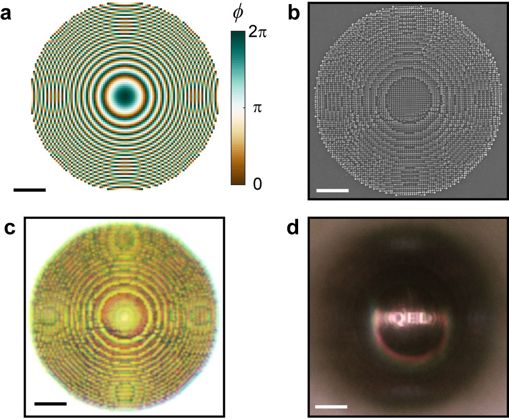
The metalens is fabricated using electron beam lithography and O2-based dry etching to produce the subwavelength pillars seen in the inset of Fig. 1a. These pillars approximate a desired continuous phase profile, , on a square grid, by mapping the pillar diameter, , to the effective refractive index, , of the lowest-order Bloch-mode supported by the pillar (Fig. 1b). We use a Fresnel lens phase profile in conjunction with Fig. 1b to assign a pillar diameter to each grid point. The discretized phase profile for a focal length at is shown in Fig. 2a, with a corresponding SEM image of the fabricated structure shown in Fig. 2b. The pillars are inherently anti-reflective (see supporting information), which is evidenced by the bright-field reflection microscope image of the metalens surface shown in Fig. 2c. To demonstrate that the structure operates as a lens, in Fig. 2d we use a transmission microscope to form an image through the metalens of a chromium shadow mask below the diamond (see supporting information).
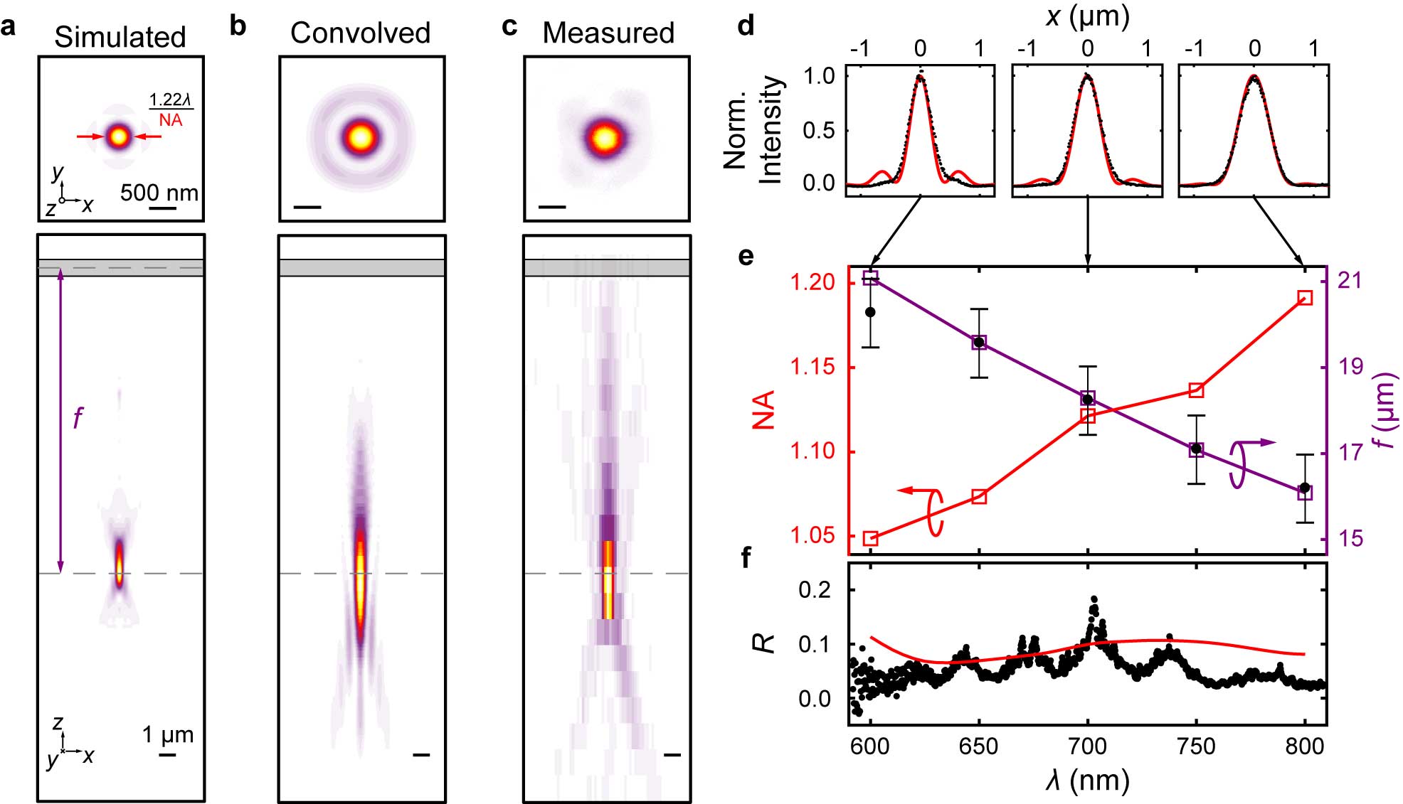
We characterize the metalens using a combination of three-dimensional full-field electromagnetic simulations and confocal microscopy. When illuminated by a plane wave in air, the metalens forms a focused spot in the diamond as shown by the simulations in Fig. 3a. We measure the focused field distribution by illuminating the metalens from above with a collimated laser beam, while imaging the transmitted field using a scanning confocal microscope with an oil immersion objective situated below the diamond. Spherical aberrations caused by imaging through the -thick diamond plate limit the resolution of these measurements, resulting in a focus spot that appears larger than the physical field profile inside of the diamond. To accurately compare simulations and measurements, we numerically model the microscope’s point-spread function (see Methods) and coherently convolve it with the simulated focus spot to predict the measured transverse and axial field profiles (Fig 3b). These predicted field profiles show excellent agreement with the measurements in Fig. 3c, as evidenced by the cross-sections shown in Fig. 3d for multiple wavelengths. Similar agreement is observed between simulations and measurements of the metalens focal length, (Fig. 3e).
The widths of the simulated field profiles are used to determine the NA of the metalens as a function of wavelength (Fig. 3e), showing across all wavelengths of the NV’s full emission spectrum. It is worth noting that the high NA of our metalens is achieved by using diamond as an immersion medium, whereas previous high-NA metalenses have relied on diffraction far from the the optical axis to focus wide angles Lee et al. (2002); Khorasaninejad et al. (2016a). This implies that the NA of our diamond design metalens could be substantially increased to values approaching the maximum by using higher-order diffraction to focus larger angles. In addition to exhibiting a high NA, the low reflectivity seen in Fig. 2c is quantified by the simulation and measurement to be below 11.5% (Fig. 3f).
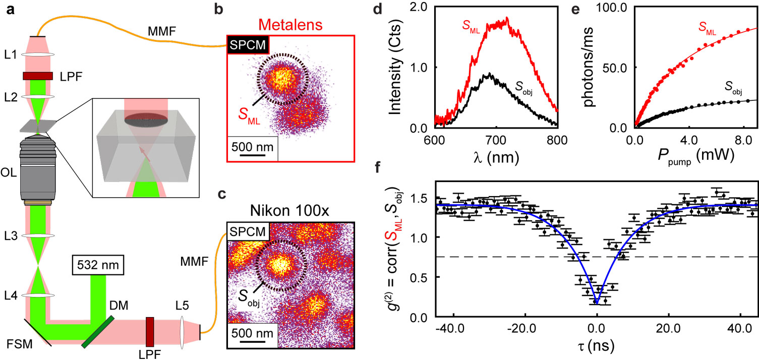
To image an NV center with the metalens, we focus a pump beam through the backside of the substrate using an oil immersion objective (Fig. 4a). The confocal collection/excitation volume of the objective is axially positioned in the plane of the metalens focus, and is rastered using a fast steering mirror (FSM). NV PL at each scan position is simultaneously measured by two fiber-coupled single-photon counting modules (SPCMs): one aligned to the metalens, and the other aligned to the confocal path through the objective. The counts collected by the SPCMs at each point of the FSM raster scan form the images shown in Fig. 4b,c. The lenses in the metalens path (L1,L2 in Fig. 4a) re-collimate the diverging metalens output beam so that a long-pass filter (LPF) can be inserted to block the pump beam. Alternatively, the metalens output can be coupled directly into a fiber, if the pump beam is removed using a different excitation geometry or a commercially-available multilayer-coated fiber tip (Omega Optical, Inc., for example).
Figures 4b and 4c both exhibit a bright spot at the same lateral position, denoted by the black dashed circles. We fix the FSM position at the center of this spot and measure the PL signals () through the metalens and objective paths, respectively. Background signals are separately recorded from a position off the spot but within the metalens field of view (see supporting information). The background-subtracted spectra of both paths (Fig. 4d) clearly exhibit the NV center’s zero-phonon line at and characteristic phonon side band. Background-subtracted PL saturation curves (Fig. 4e) display saturation count rates of photons/ms and photons/ms when measured through the metalens and objective, respectively. The ratio of saturation count rates provides an estimate for the metalens collection efficiency, further indicating that the metalens has NA (see Methods). Finally, we measure the second-order cross-correlation function, , between both paths. The background-corrected measurements (Fig. 4f) exhibit the characteristic antibunching dip and short-delay bunching of a single NV center, clearly demonstrating that the spots in Fig. 4b,c are indeed the same single-photon emitter.
The diamond immersion metalens lays the foundation for packaging quantum emitters in high-refractive-index substrates, as it has the potential to significantly improve emitter collection efficiency and simplify experiments by replacing the objective/SIL combination typically used for imaging quantum emitters in a cryostat. This approach can be directly applied to other quantum-emitter-host materials including silicon carbide, III-V semiconductors, and oxides. Leveraging the structure’s high transmission efficiency and scalable top-down fabrication, other metasurface phase profiles can be explored to further increase the metalens NA by designing for large-angle diffraction Lee et al. (2002), co-focusing pump and PL wavelengths Wang et al. (2016); Ribot et al. (2013), shaping emission from quantum emitter ensembles Lawrence, Trevino, and Dal Negro (2012), and as a means for compensating mismatches between emitters and surface orientations Backlund et al. (2016). In addition, this type of metasurface could be incorporated with nanophotonic structures for Purcell enhancement, for example to collimate the output of a chirped surface grating structure through the backside of the diamondZheng et al. (2017), or to extend the cavity length of a fiber-based resonator cavity Bogdanović et al. (2017). Dielectric metasurface design will lead to compact, fiber-coupled single-photon sources and quantum memories, with other potential applications to diffractive optics for space Nikolajeff and Karlsson (2013) and Raman lasers Mildren et al. (2013).
Acknowledgements
This work was supported by an NSF CAREER grant (ECCS-1553511), the University Research Foundation, and the Singh Center for Nanotechnology at the University of Pennsylvania, a member of the National Nanotechnology Coordinated Infrastructure (NNCI), which is supported by the National Science Foundation (Grant ECCS-1542153). S.A.M. and E.C.G. were supported by the Netherlands Organisation for Scientific Research (NWO) and the European Research Council under the European Union’s Seventh Framework Programme ((FP/2007-2013)/ERC grant agreement no. 337328, “Nano-EnabledPV”).
Author contributions
R. R. G. and T.-Y. H. contributed equally to this work. R. R. G. and L. C. B. conceived of the project. R. R. G., S. A. M., and E. C. G. performed the design and simulations; R. R. G. and G. G. L. fabricated the metalens; R. R. G., T.-Y. H., D. A. H., A. L. E., and L. C. B. performed the measurements and analysis. All authors contributed to writing the manuscript.
Methods
Design. The metalens was designed using the procedure devised by Lalanne et al. for TiO2 deposited on glass Lalanne et al. (1999). The procedure was carried out as follows: First, the Bloch-mode effective index, , was calculated as a function of pillar diameter (Fig. 1b) on a subwavelength grid. The grid-pitch, , was chosen to be just below the onset of first order diffraction, at , which was rounded up to . The pillar height was chosen to be and the minimum pillar diameter was set to to ensure compatibility with our fabrication process. The maximum pillar diameter, , was then found by determining the required to achieve an optical pathlength increase of relative to the minimum pillar diameter:
| (1) |
The corresponding is found from the dispersion curve in Fig. 1b. The minimum and maximum pillar diameters are indicated in Fig. 1b (black dashed lines) along with the their relative optical pathlengths (red dashed lines).
The Fresnel phase profile in Fig. 2a was calculated by , with 93 grid points for a diameter of measured by the grid edges at the maximum widths along the Cartesian design dimensions. The symmetry of this structure ensures polarization independent focusing, which has been shown for similar designs using TiO2 deposited on glass Khorasaninejad et al. (2016b).
Fabrication. The metalens was fabricated on double-side polished high-pressure/high-temperature (HPHT)-grown single-crystal diamond (Applied Diamond, Inc.). The diamond surface was cleaned in Nano-Strip (a stabilized mixture of sulfuric acid and hydrogen peroxide, Cynaktec KMB 210034) for , followed by a plasma clean in a barrel asher with 40 sccm O2 and RF power. The metalens pattern was proximity effect corrected (see supporting information) and written in hydrogen silsesquioxane (HSQ, Dow Corning, Fox-16) using a 50 keV electron beam lithography tool (Elionix, ELS-7500EX). Prior to spin-coating HSQ, a adhesion layer of SiO2 was deposited on the diamond surface by electron beam evaporation to promote adhesion. After exposure, the pattern was developed in a mixture of deionized water with of sodium chloride and of sodium hydroxide Yang and Berggren (2007). Our e-beam lithography process for HSQ on diamond can be found in ref. Grote, Bassett, and Lopez, 2016. A reactive ion etch (RIE, Oxford Instruments, Plasma lab 80) was used to remove the SiO2 adhesion layer and to transfer the HSQ pattern into the diamond surface. The SiO2 adhesion layer was removed by a CF4 reactive ion etch Metzler (2016), followed by a O2 RIE etch with a flow rate of 40 sccm, a chamber pressure of , and an RF power of to form the diamond pillars. Finally, the HSQ hardmask was removed using buffered-oxide etch.
Simulations. Calculations of , (Fig. 1b, left and right axes, respectively), and pillar transmission efficiency (supporting information) were performed using 3D rigorous coupled-wave analysis (RCWA) based on the method developed by RumpfRumpf (2011). The effective index of the pillars was calculated by solving for the eigenvalues of Maxwell’s equations with the -invariant refractive index profile of the pillar cross-section in a square unit cell at . The eigenproblem was defined in a truncated planewave basis using planewaves, with implicit periodic boundary conditions. Following these calculations, the pillar height was set to with air above and homogeneous diamond below, and the complex amplitude transmission coefficient, , of a normal incidence planewave from air is calculated as a function of pillar diameter. The right axis of Fig. 1b was found by .
The focused spot in Fig. 3a was calculated using 3D finite-difference time-domain simulations (FDTD, Lumerical Solutions, Inc.). The -diameter metalens is contained in a total-field/scattered-field (TFSF) excitation source to reduce artifacts caused by launching a planewave into a finite structure. Perfectly matched layers (PMLs) were used as boundary conditions away from the TFSF source. The simulation mesh in the pillars was set to , increasing gradually to along the propagation ()-direction into the diamond. Diamond is modeled with a non-dispersive refractive index, . An -polarized planewave pulse () is launched from air toward the metalens surface. Steady-state spatial electric field distributions, , at five wavelengths ranging from were stored, and the spatial fields at are plotted as transverse () and axial () intensity distributions in Fig. 3a. The focal length, , at each wavelength (Fig. 3e) was determined by finding the grid point in the simulation cell where is maximum. The spatial distribution of the steady-state field amplitude, , in Fig. 1a was simulated by removing the TFSF source and placing an -oriented dipole current source at the metalens focus position with a wavelength of . The reflection spectrum (Fig. 3f) was calculated by integrating the time-averaged Poynting vector, , over a surface, above and below the metalens within the TFSF source volume. The simulation volume was reduced to and the number of wavelength points was increased to 41 for these simulations.
The images in Fig. 3b represent the optical intensity, , collected by a detector at a focus position in the sample, , defined by the FSM in the transverse directions and by the sample stage in the axial direction: . These images are produced by coherently convolving the FDTD-calculated steady-state fields, , with the point-spread function (PSF) of the microscope, which is modeled by numerically evaluating the diffraction integrals, , that define the dyadic Green’s function of a high-NA optical system Novotny and Hecht (2006):
| (5) | ||||
| (9) |
with the inclusion of an aberration function that accounts for the optical pathlength difference introduced by imaging through a media with mismatched refractive indices Sheppard and Török (1997) ( and for our measurement setup). We assume an infinitesimal pinhole, which is consistent with our imaging system being below the confocal condition (see supporting information). Using Eqn. (9), the image formed by our microscope is modeled in the following manner (see supporting information):
| (10) |
where denotes a three-dimensional spatial convolution. The transverse, , and axial, , image intensity distributions at are shown in Fig. 3b, and cross-sections, , at are plotted in Fig. 3d (red curves). Transverse profiles at five wavelengths ranging from are plotted in the supporting information.
Experimental. Measurements of the metalens were carried out with a custom-built confocal microscope, comprised of an oil immersion objective with adjustable iris (Nikon Plan Fluor x100/0.5-1.30) and an inverted optical microscope (Nikon Eclipse TE200) with a -axis piezo stage (Thorlabs MZS500-E) as well as a scanning stage for the - and -axis (Thorlabs MLS203-1). The diamond host substrate was fixed to a microscope coverslip (Fisher Scientific 12-548-C) using immersion oil (Nikon type N) with the patterned surface facing upwards. A combination of cage system and SM1-thread components (Thorlabs) were used to create a fiber-coupled optical path above the stage of the inverted microscope. This configuration allowed for simultaneous excitation and measurement of the metalens from air (fiber-coupled path) or through diamond (objective path). The objective path was routed outside of the microscope body so that laser-scanning confocal excitation and collection optics could be added. A relay-lens-system consisting of two achromatic doublet lenses (Newport, focal length, PAC058AR.14) is used to align the back aperture of the objective to a fast-steering mirror (FSM, Optics in motion, OIM101), which is used to raster the diffraction-limited confocal volume in the transverse plane of the objective space. A long-pass dichroic mirror (Semrock, BrightLine FF560-FDi01) placed after the FSM was used to couple a excitation laser (Coherent, Compass 315M-150) into the objective, while wavelengths above pass through the dichroic mirror and are focused into a -core, 0.1 NA, multimode fiber (Thorlabs M67L01) that can be connected to a single-photon counting module (Excelitas, SPCM-AQRH-14-FC) or a spectrometer (Princeton Instruments IsoPlane-160, blaze wavelength with 1200 G/mm) with a thermoelectrically-cooled CCD (Princeton Instruments PIXIS 100BX). Computer control of the FSM and counting the electrical output of the SPCM are achieved using a data acquisition card (DAQ, National Instruments PCIe-6323).
For the characterization measurements presented in Fig. 3, a broadband supercontinuum source (Fianium WhiteLase SC400) was coupled into a single-mode fiber (Thorlabs P1-630AR-2), which was used to illuminate the metalens from the fiber-coupled path of our microscope. A collimating lens (Thorlabs CFC-2X-A) was used to create a diameter Gaussian beam that emulates the planewave source used in our FDTD simulations. The excitation wavelength is set by passing the supercontinuum beam through a set of linear variable short-pass (Delta Optical Thin Film, LF102474) and long-pass filters (Delta Optical Thin Film LF102475) prior to fiber-coupling, which can be adjusted to filter out a single wavelength with bandwidth or be removed completely for broadband excitation. The transverse profile and cross-sections in Fig. 3c,d were measured by filtering the supercontinuum source to a single wavelength and rastering the FSM while collecting counts in the SPCM connected to the confocal path at each scan position. This process is repeated for a series of -stage positions to measure the axial profile, which is shown in Fig. 3c at and was used to find the metalens focal length as a function of wavelength in Fig. 3e. For reflection measurements (Fig. 3f) a achromatic lens (Thorlabs AC064-015-B) is used to focus the collimated excitation beam to a -diameter spot at the top surface of the diamond. A beamspliter cube (Thorlabs BS014) was added between the collimating and focusing lenses so that reflected light could be focused into a -core MMF (Thorlabs, M25L01) that is coupled to a spectrometer (Thorlabs CCS100) using a achromatic doublet lens (Newport, PAC052AR.14).
In Fig. 4, the fiber-coupled path was used to image a single NV center through the metalens, as shown in Fig. 4a. This was achieved with two achromatic doublet lenses (L1 & L2) with focal lengths of and (Thorlabs AC064-013/015-B), respectively, aligned to a -core, 0.1 NA, multimode fiber (Thorlabs M67L01). The multimode fiber was then connected to a second SPCM (Excelitas, SPCM-AQRH-14-FC), allowing for simultaneous PL collection from both the fiber-coupled and objective paths while scanning the excitation source. The long-pass filters (LPF) in both collection lines consisted of a and a long-pass filters (Semrock, EdgeBasic BLP01-532R, EdgeBasic BLP01-568R) for spectra measurements, with an additional long-pass filter (Thorlabs, FEL0650) in both paths to improve the signal-to-background for PL, saturation, and cross-correlation measurements. The outputs of both SPCMs were connected to a time-correlated single-photon counting card (TCSPC, PicoQuant, PicoHarp 300) to collect photon arrival-time data that was used to calculate cross-correlation functions (Fig. 4f). Background spectra and saturation curves were measured at a transverse scan position away from the NV, but still within the field-of-view of the metalens, and were subtracted from measurements taken on the NV. This process was also used to determine the background for correcting cross-correlation data by interleaving 40 measurements off the NV with 40 measurements taken on the NV, each with a acquisition time. Further details on background-subtraction of the measurements in Fig. 4 are given in the supporting information.
Analysis. The NA of the metalens, NA, plotted in Fig. 3e is calculated by fitting the simulated transverse focus spot at each wavelength to the paraxial point-spread function of an ideal lens, an Airy disk Novotny and Hecht (2006),
| (11) |
where is the free space wavenumber and is the radial coordinate in the focal plane. Fits are performed using non-linear least squares curve fitting (MATLAB function lsqcurvefit). The entrance pupil, , of the metalens can be calculated by geometry using NA and :
| (12) |
Using Fig. 3e along with eqn. (12), we find that , which is smaller than the physical diameter of the metalens. This indicates a maximum collection angle inside the diamond of . Despite this limited collection angle, Fig. 3e clearly illustrates NA, which can be increased by using diffractive designs for larger angles.
The focal length of the metalens in Fig. 3e was determined by measuring the distance between the metalens surface and the focused spot formed below the metalens using the piezo stage of the microscope. The distance traversed by the piezo stage is then scaled by a factor of to compensate for distortions caused by imaging through diamond Visser and Oud (1994). Further details are given in the supporting information.
The reflectance spectrum in Fig. 3f was normalized using measurements of the reflected optical power measured with the fiber-coupled path aligned to the metalens, , and off the metalens on a planar region of the diamond surface, , using the following expression:
| (13) |
where is the reflectance of an air/diamond interface and is calculated using Fresnel coefficients to be at normal incidence. The ripples in Fig. 3f are due to ghosting from the beam splitter cube used to collect the reflected signal (see supporting information). The measured reflectance spectrum is slightly lower than the simulated spectrum (both plotted in Fig. 3f). The source of the discrepancy is believed to be due to the NA of our top collection optics. The simulations represent the reflected light over all angles (specular and scattered), while our collection optics only cover a limited range of angles.
The saturation curves in Fig. 4e were fit with the following equation:
| (14) |
using non-linear least squares curve fitting (MATLAB function lsqcurvefit), resulting in saturation count rates of photons/ms and photons/ms for the metalens signal, , and confocal signal, , respectively. The saturation power was in both paths, since they are both pumped by the same excitation beam.
The collection efficiency as a function of numerical aperture can be estimated as Castelletto et al. (2011):
| (15) |
Assuming that the excitation and collection paths have similar transmission efficiencies, the ratio of collection efficiencies from both paths is equal to the ratio of saturation count rates, . Using a numerical aperture of NA for the confocal collection path, the metalens is estimated to have NA. If instead we assume that the ratio of the collection efficiencies is proportional to the ratio of the integrated spectra in Fig. 4d, we find that NA. Discrepancies in these values arise from differences in the collection efficiency of both paths caused by the confocal aperture and optical components in the path. However, this rough calculation provides strong evidence that NA.
Background-correction of the cross-correlation data in Fig. 4f was performed using the following relationship(Brouri et al., 2000):
| (16) |
where is the measured second-order correlation function and is the total signal-to-background ratio determined by 40 repeated measurements. After background correction, is fit with the following expression:
| (17) |
which corresponds to the the approximation of the NV center as a 3-level structureKitson et al. (1998). The fit coefficients are as follows: . Further details are given in the supporting information.
References
References
- Aharonovich, Englund, and Toth (2016) I. Aharonovich, D. Englund, and M. Toth, Nature Photonics 10, 631 (2016).
- Gao et al. (2015) W. Gao, A. Imamoglu, H. Bernien, and R. Hanson, Nature Photonics 9, 363 (2015).
- Rondin et al. (2014) L. Rondin, J. Tetienne, T. Hingant, J. Roch, P. Maletinsky, and V. Jacques, Reports on progress in physics 77, 056503 (2014).
- Balasubramanian et al. (2014) G. Balasubramanian, A. Lazariev, S. R. Arumugam, and D.-W. Duan, Current opinion in chemical biology 20, 69 (2014).
- Awschalom et al. (2013) D. D. Awschalom, L. C. Bassett, A. S. Dzurak, E. L. Hu, and J. R. Petta, Science 339, 1174 (2013).
- Aharonovich and Neu (2014) I. Aharonovich and E. Neu, Advanced Optical Materials 2, 911 (2014).
- Lončar and Faraon (2013) M. Lončar and A. Faraon, MRS bulletin 38, 144 (2013).
- Faraon et al. (2013) A. Faraon, C. Santori, Z. Huang, K.-M. C. Fu, V. M. Acosta, D. Fattal, and R. G. Beausoleil, New J. Phys. 15, 025010 (2013).
- Schröder et al. (2016) T. Schröder, S. L. Mouradian, J. Zheng, M. E. Trusheim, M. Walsh, E. H. Chen, L. Li, I. Bayn, and D. Englund, JOSA B 33, B65 (2016).
- Ofori-Okai et al. (2012) B. Ofori-Okai, S. Pezzagna, K. Chang, M. Loretz, R. Schirhagl, Y. Tao, B. Moores, K. Groot-Berning, J. Meijer, and C. Degen, Physical Review B 86, 081406 (2012).
- Chu et al. (2014) Y. Chu, N. P. de Leon, B. J. Shields, B. Hausmann, R. Evans, E. Togan, M. J. Burek, M. Markham, A. Stacey, A. S. Zibrov, et al., Nano letters 14, 1982 (2014).
- Castelletto et al. (2011) S. Castelletto, J. Harrison, L. Marseglia, A. Stanley-Clarke, B. Gibson, B. Fairchild, J. Hadden, Y. D. Ho, M. Hiscocks, K. Ganesan, et al., New J. Phys. 13, 025020 (2011).
- Hensen et al. (2015) B. Hensen, H. Bernien, A. E. Dréau, A. Reiserer, N. Kalb, M. S. Blok, J. Ruitenberg, R. F. Vermeulen, R. N. Schouten, C. Abellán, et al., Nature 526, 682 (2015).
- Jechow et al. (2011) A. Jechow, E. Streed, B. Norton, M. Petrasiunas, and D. Kielpinski, Optics letters 36, 1371 (2011).
- Kildishev, Boltasseva, and Shalaev (2013) A. V. Kildishev, A. Boltasseva, and V. M. Shalaev, Science 339, 1232009 (2013).
- Yu and Capasso (2014) N. Yu and F. Capasso, Nature materials 13, 139 (2014).
- Lalanne and Chavel (2017) P. Lalanne and P. Chavel, Laser & Photonics Reviews 11 (2017).
- Genevet et al. (2017) P. Genevet, F. Capasso, F. Aieta, M. Khorasaninejad, and R. Devlin, Optica 4, 139 (2017).
- Khorasaninejad et al. (2016a) M. Khorasaninejad, W. T. Chen, R. C. Devlin, J. Oh, A. Y. Zhu, and F. Capasso, Science 352, 1190 (2016a).
- Lee et al. (2002) M.-S. L. Lee, P. Lalanne, J. Rodier, P. Chavel, E. Cambril, and Y. Chen, Journal of Optics A: Pure and Applied Optics 4, S119 (2002).
- Chang-Hasnain and Yang (2012) C. J. Chang-Hasnain and W. Yang, Advances in Optics and Photonics 4, 379 (2012).
- Vo et al. (2014) S. Vo, D. Fattal, W. V. Sorin, Z. Peng, T. Tran, M. Fiorentino, and R. G. Beausoleil, IEEE Photonics Technology Letters 26, 1375 (2014).
- Wang et al. (2016) B. Wang, F. Dong, Q.-T. Li, D. Yang, C. Sun, J. Chen, Z. Song, L. Xu, W. Chu, Y.-F. Xiao, et al., Nano letters 16, 5235 (2016).
- Ribot et al. (2013) C. Ribot, M.-S. L. Lee, S. Collin, S. Bansropun, P. Plouhinec, D. Thenot, S. Cassette, B. Loiseaux, and P. Lalanne, Advanced Optical Materials 1, 489 (2013).
- Lawrence, Trevino, and Dal Negro (2012) N. Lawrence, J. Trevino, and L. Dal Negro, Journal of Applied Physics 111, 113101 (2012).
- Backlund et al. (2016) M. P. Backlund, A. Arbabi, P. N. Petrov, E. Arbabi, S. Saurabh, A. Faraon, and W. Moerner, Nature photonics 10, 459 (2016).
- Zheng et al. (2017) J. Zheng, A. C. Liapis, E. H. Chen, C. T. Black, and D. Englund, arXiv preprint arXiv:1706.07566 (2017).
- Bogdanović et al. (2017) S. Bogdanović, S. B. van Dam, C. Bonato, L. C. Coenen, A.-M. J. Zwerver, B. Hensen, M. S. Liddy, T. Fink, A. Reiserer, M. Lončar, et al., Applied Physics Letters 110, 171103 (2017).
- Nikolajeff and Karlsson (2013) F. Nikolajeff and M. Karlsson (Wiley Online Library, 2013) Chap. 4, pp. 109–142.
- Mildren et al. (2013) R. P. Mildren, A. Sabella, O. Kitzler, D. J. Spence, and A. M. McKay, in Optical Engineering of Diamond, edited by R. P. Mildren and J. R. Rabeau (Wiley Online Library, 2013) Chap. 8, pp. 239–276.
- Lalanne et al. (1999) P. Lalanne, S. Astilean, P. Chavel, E. Cambril, and H. Launois, JOSA A 16, 1143 (1999).
- Khorasaninejad et al. (2016b) M. Khorasaninejad, A. Zhu, C. Roques-Carmes, W. Chen, J. Oh, I. Mishra, R. Devlin, and F. Capasso, Nano letters 16, 7229 (2016b).
- Yang and Berggren (2007) J. K. Yang and K. K. Berggren, Journal of Vacuum Science & Technology B: Microelectronics and Nanometer Structures Processing, Measurement, and Phenomena 25, 2025 (2007).
- Grote, Bassett, and Lopez (2016) R. R. Grote, L. C. Bassett, and G. G. Lopez, “High contrast 50kV e-beam lithography for HSQ atop diamond using ESPACER for spin-on charge dissipation,” http://repository.upenn.edu/scn_protocols/21/ (2016), accessed: 2017-10-31.
- Metzler (2016) M. Metzler, “Reactive ion etch (RIE) of silicon dioxide (SiO2) with tetrafluoromethane (CF4),” http://repository.upenn.edu/scn_tooldata/36/ (2016), accessed: 2017-10-31.
- Rumpf (2011) R. C. Rumpf, Progress In Electromagnetics Research B 35, 241 (2011).
- Novotny and Hecht (2006) L. Novotny and B. Hecht, Principles of nano-optics (Cambridge university press, 2006).
- Sheppard and Török (1997) C. J. R. Sheppard and P. Török, Journal of microscopy 185, 366 (1997).
- Visser and Oud (1994) T. Visser and J. Oud, Scanning 16, 198 (1994).
- Brouri et al. (2000) R. Brouri, A. Beveratos, J.-P. Poizat, and P. Grangier, Optics letters 25, 1294 (2000).
- Kitson et al. (1998) S. Kitson, P. Jonsson, J. Rarity, and P. Tapster, Physical Review A 58, 620 (1998).