Heavy and light hole minority carrier transport properties in low-doped n-InGaAs lattice matched to InP
Abstract
Minority carrier diffusion lengths in low-doped n-InGaAs using InP/InGaAs double-heterostructures are reported using a simple electrical technique. The contributions from heavy and light holes are also extracted using this methodology, including minority carrier mobilities and lifetimes. Heavy holes are shown to initially dominate the transport due to their higher valence band density of states, but at large diffusion distances, the light holes begin to dominate due to their larger diffusion length. It is found that heavy holes have a diffusion length of µm for an n-InGaAs doping of at room temperature, whereas light holes have a diffusion length in excess of µm. Heavy holes demonstrate a mobility of and a lifetime of µs, whereas light holes demonstrate a mobility of and a slightly longer lifetime of µs. The presented method, which is limited to low injection conditions, is capable of accurately resolving minority carrier transport properties.
Minority carrier diffusion lengths are critically influential in optoelectronic device performance, including solar cells, photodetectors and heterojunction bipolar transistors for example. Several methods presently exist to measure these, including electron beam induced current (EBIC) along a cross-sectional pn junction,Maximenko cathodoluminescence (CL) measurements on double-heterostructures,Schultes ; Gustafsson ; Niemeyer zero-field time-of-flightSharma ; Lovejoy , surface phovotoltageScroder ; Kronik to name a few. Coupling these diffusion lengths to lifetime measurements typically obtained from time-resolved photoluminescence, time-of-flight experiments, or time-resolved CL measurements,Boulou one can then infer minority carrier mobilities if both measurements are performed for a comparable excess carrier concentration. These parameters can be critical in designing minority carrier devices, for example in cases where minority carrier mobilities exceed that of majority carrier mobilitiesLovejoy or in solar cells where minority carrier diffusion lengths are on the order of the active region thickness.Walkera
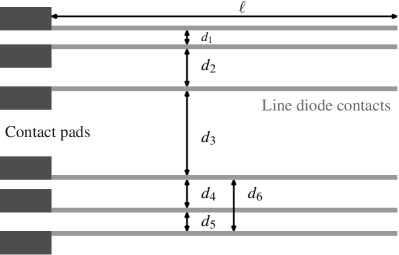 |
Each of the aforementioned methodologies have their inherent advantanges and disadvantages. For example, the zero-field time-of-flight method is simple in principle, but becomes obfuscated when fitting the transient photovoltage for a heterojunction such as an InP/InGaAs photodetector. For cross-sectional EBIC, the method can be destructive since samples must be well polished for a clean cross-section, and the requirement of an electron microscope can result in significant time and effort. Thus it is of interest to develop an overall simpler method to measure minority carrier diffusion lengths. Here, we present a purely electrical method capable of extracting diffusion lengths that is effectively a steady-state Haynes Shockley experiment.Haynes ; Shockley The method is demonstrated using an n-type InP:Si/intrinsic InGaAs/n-type InP:Si double-heterostructure which is used to make pin short wave infrared detectors and focal plane arrays.Walkerb Furthermore, this method is shown to be capable of separating the contributions of heavy and light holes, and, with a few assumptions, determining the lifetimes and diffusion constants (i.e. mobilities). The required test devices can also be included on production wafers to monitor the material and fabrication quality across the wafer and from epitaxial run to run. These test structures consist of long (µm) and thin (µm) diffused junction line diodes as shown in Fig. 1. The junction is created by Zn diffusion through the InP and about nm into the InGaAs material. The inter-line diode separations range from much shorter to much longer than the diffusion length. Note that, during the measurement, one can bypass one diode to obtain a larger distance, as illustrated by in Fig. 1.
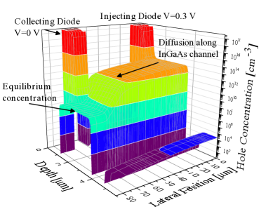
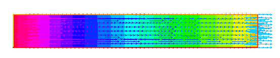
The basic physics is summarized in detail elsewhere.Walkerb ; Sze Essentially, forward biasing one line diode injects minority carriers into the InGaAs layer leading to diffusion of carriers through the InGaAs channel. This can be seen in Fig. 2 showing a simulated cross-section of the device in terms of hole concentration as a function of depth and lateral position between two adjacent line diodes using Atlas by Silvaco (v.5.23.12.C), assuming default material properties.AtlasUG The hole concentration is uniform across the thickness of the InGaAs layer since its thickness (µm) is significantly smaller than the diffusion length. The carriers which diffuse to an adjacent line diode are collected by applying a zero or slightly reverse bias with respect to the bottom InP layer which serves as the ground contact. Assuming low injection, if the length of the line diode is sufficiently long compared to the maximum interdiode distance , and if is much longer than the InGaAs thickness, the hole current can be described by the one dimensional diffusion equation. The hole density under the injecting diode is , which is dictated by the applied bias, and the hole concentration at the collecting diode is the equilibrium value since the collecting diode is maintained at zero applied bias. Using these boundary conditions, and assuming no interface recombination, solving the diffusion equation leads to the solution in terms of the collected hole current density as a function of interdiode separation given asWalkerb ; Sze
| (1) |
where is the diffusion length, is the diffusion coefficient, is the mobility, is Boltzmann’s constant, is temperature and is the electronic charge. In the case of low injection, the initial (injected) hole density can be calculated using ), where is the intrinsic carrier concentration and is the donor concentration in the InGaAs extracted using CV measurements on µm diameter devices. Finally, is the equilibrium hole concentration given by . Note the cross-sectional area used to scale the measured current to a current density is given by , where is the InGaAs thickness and is the length of the diode. Fitting Eq. (1) to experimental data thus reveals the minority carrier diffusion length and the mobility , thus giving access to the lifetime . An electron effective mass of is assumed for InGaAs, along with heavy and light hole effective masses of and respectively, and a room temperature bandgap of 0.734 eV.Vurgaftman This gives an intrinsic carrier concentration of for room temperature (T=K).
However, an important consideration that is easy to overlook is the interdiode separation . The simulation results of Fig. 2 shows that the hole concentration is nearly constant under the injecting diode, but starts decreasing by within µm of the inside edge of the diode. On the other hand, the hole concentration drops rapidly to the equilibrium concentration from the leading edge of the collecting diode. The separation of the diodes therefore starts a small distance inside the edge of the injecting diode and ends some distance past the leading edge of the collecting diode. This separation correction, , to the interdiode separation , defined from the inner edges of two diodes, is discussed later.
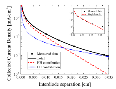
Current - voltage measurements were made using a Hewlett-Packard HP4155C Semiconductor Analyzer. Results from devices from two different wafers than the device reported here were reported in Ref. 13 and are similar to the present results. A fit to measured collected current densities for an applied bias of 0.3V to Eq. (1) with fitting parameters µm and is shown in the inset of Fig. 3, assuming a separation correction of µm. The measured collected current for the largest separation of µm is well above the theoretical fit, and the point at µm is also above, albeit slightly. These higher than expected currents at large diffusion distances can be explained by the existance of light holes with a longer diffusion length than heavy holes.
In order to account for both heavy and light holes, two versions of Eq. (1), one for heavy holes and one for light holes, can be added together to give the total collected current. The number of fitting parameters doubles, which can lead to more ambiguity in the fit. One must first calculate the fraction of the injected hole concentration composed of heavy holes, , which is dictated by the ratio of heavy hole density of states to the total valence band density of states (ignoring the split-off band), given as
| (2) |
the fraction for light hole occupation is analogous, or simply given as . For the adopted heavy and light holes effective masses, heavy holes dominate the valence band density of states by a factor of .
The best fit of Eq. (1) for the sum of heavy and light holes, as well as their individual contributions, are illustrated in Fig. 3 for an applied bias of 0.3 V. The fit is achieved using a nonlinear least squares fitting algorithm from Matlab R2017a’s curve fitting toolbox. The algorithm uses the diffusion length and diffusion constant for both light and heavy holes respectively as fitting parameters. Standard errors for the best-fit parameters are computed using the mean square errors and the Jacobian matrix at the solution (i.e. neglecting the higher order terms to approximate the Hessian matrix, which is reasonable since the residuals are close to zero at the solution). It is clear that adding a term specifically for the light holes yields a much better agreement for the largest interdiode separations. The heavy and light hole diffusion lengths are extracted as and respectively, again assuming a separation correction of µm. These can be compared to the diffusion length of found using the single carrier model. This single carrier value thus represents an effective diffusion length, combining both a shorter heavy hole diffusion length and a longer light hole diffusion length. These diffusion lengths are within the range of previously determined diffusion lengths at room temperature of µm for a lower doping of .Gallant From the results in Fig. 3, for short interdiode separations, the current is mainly due to heavy holes; in particular, for , of the current is due to heavy hole transport. This decreases to at µm, beyond which light holes dominate the transport. For minority carrier devices such as InGaAs/InP pnp transistors, light holes can contribute of the diffusion current.
It is important now to discuss the influence of the separation correction to the interdiode separation on the extracted diffusion length. For example, setting this to µm results in a heavy hole µm (a increase) and light hole µm (a increase); note the large uncertainties. Exceeding µm further decreases the diffusion lengths, but also increases the uncertainties. A value of µm is thus used in the remaining analysis, and is assumed to stay constant as a function of separation.
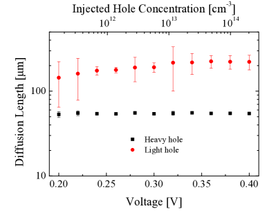
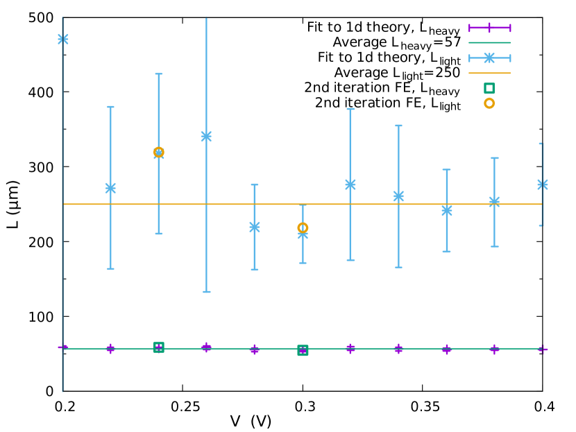
The fitting can be performed as a function of voltage to investigate the injection level dependence of the diffusion lengths for this sample. This also tests the ability of the method to extract consistent parameters. The results are illustrated in Fig. 4, where the applied bias is shown on the bottom axis and the corresponding injected hole concentration is shown on the top axis. One can observe a near constant diffusion length across the voltage range of V for the heavy holes, which validates the robustness of the method. The light holes, however, show a trend of increasing diffusion length for increasing voltage, although it could be considered constant within the error bars. This may be due to the choice of the separation correction value, and/or by assuming that it is constant as a function of separation. It is further complicated by the random error in the current measurement. Improving the determination of the correction factor requires further investigation using careful device simulations. The standard deviation for heavy hole diffusion lengths () is significantly smaller than for light holes (). This is due to the heavy hole parameter fitting being based on sufficient data points, whereas light hole parameters rely on mainly the last two data points. More data points for larger interdiode separations would improve the accuracy of the extracted light hole diffusion lengths, and this may clarify the observed trend of increasing for increasing voltage. Lastly, the standard error is observed to vary considerably depending on the fit (even if it appears good by eye), and this is due to current measurement errors. Overall, the light hole diffusion lengths are longer than the heavy hole diffusion lengths, which is a result of the larger light hole mobility (discussed next). Also, increasing the hole injection beyond V leads to a breakdown of the model’s low injection assumption. Lastly, fitting at sufficiently low voltage (V) results in large uncertainties due to the significant scatter in the data arising from hysteresis in the the current measurement and the overall high noise in measuring currents below 10 pA. Improving the accuracy of the current measurement would result in more accurate diffusion length parameters.
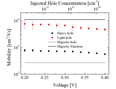
The minority carrier mobilities are also obtained as a function of voltage from the fit to the data. The results are illustrated in Fig. 5a. The average mobilities are and for heavy and light holes respectively. The observed trends of decreasing mobility for increasing voltage were not expected. Further investigation into this is required to determine if this observation is real. Note that the mobility results depend strongly on the choice of band parameters (which dictate the calculated injection level) and temperature. The choice of separation correction primarily influences the light hole transport properties. Nevertheless, light holes are determined to be significantly more mobile than heavy holes by a factor of , which is expected based on their effective masses as well as their extracted diffusion lengths. The light hole mobility is somewhat smaller but on the same order of magnitude as the electron Hall mobility () for intrinsic material,Sotoodeh considering their similar effective masses. Interestingly, the heavy hole mobilities are considerably larger than the majority hole Hall mobility of for the corresponding sample doping level of .Sotoodeh Overall, the heavy and light hole mobilities fall within the range of hole and electron mobilities from Sotoodeh (see horizontal lines in Fig. 5a). With respect to other published data, the reported hole mobility reported here is greater than the reported by Gallant and Zemel.Gallant This emphasizes the importance of characterizing minority carrier mobilities for device design and simulation. Overall, careful temperature control is critical for this component of the study. Lastly, a better knowledge of band parameters would improve the extraction of the mobilities.
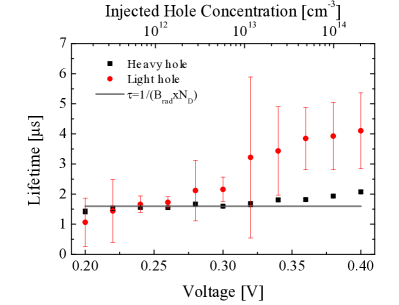
Finally, Figure 5b illustrates the extracted lifetimes for heavy and light holes as a function of injection. The heavy hole lifetime corresponds to the lifetime dictated by the radiative recombination coefficient and the doping, indicated by the horizontal line. This is in agreement with other studies conducted on low-doped InGaAs.Wichman ; Zielinski ; Wintner ; Walkerb While technically this method cannot distinguish between bulk recombination in the layer and surface recombination at the hetero junction interfaces, the apparent dominance of radiative recombination justifies the assumption of negligible surface recombination. The lifetimes for heavy holes are more accurate than those for light holes. For the device reported here, as well as other devices, the light hole lifetime appears to be longer than for heavy holes. Again, more data in the range of the largest interdiode separations would be required to improve the accuracy of the lifetime for the light holes. An independent measurement of the effective lifetime (both heavy and light holes) could also reduce the fitting parameters, thereby potentially providing better results for the diffusion length and mobility.
In conclusion, a simple and nondestructive electrical method was proposed to extract minority carrier diffusion lengths, mobilities and lifetimes using long and thin diffused double-heterostructure diodes. The proposed method was demonstrated in low-doped n-InGaAs lattice matched to InP for a sample doped to . Heavy and light hole diffusion was observed as separate contributions, with a heavy hole diffusion length of µm (averaged over injection), and a light hole diffusion length of µm. The hole mobilities were extracted to be and for heavy and light holes respectively. Ultimately, radiative recombination dominates the lifetime component, which is found to be for heavy holes and for light holes. The method is limited to low injection, and to diffusion lengths longer than the InGaAs layer thickness.
References
- (1) S. I. Maximenko, M. P. Lumb, R. Hoheisel, M. Gonzalez, D. A. Scheiman, S. R. Messenger, T. N. D. Tibbits, M. Imaizumi, T. Ohshima, S. I. Sato, P. P. Jenkins, and R. J. Walters. "Radiation response of multi-quantum well solar cells: Electron-beam-induced current analysis," Journal of Applied Physics, 118, 245705, 2015.
- (2) F. J. Schultes, T. Christian, R. Jones-Albertus, E. Pickett, K. Alberi, B. Fluegel, T. Liu, P. Misra, A. Sukiasyan, H. Yuen, and N. M. Haegel. “Temperature dependence of diffusion length, lifetime and minority electron mobility in GaInP,” Applied Physics Letters, 103, 242106 (2013).
- (3) M. Niemeyer, J. Ohlmann, A. W. Walker, P. Kleinschmidt, R. Lang, T. Hannappel, F. Dimroth and D. Lackner. "Minority carrier diffusion length, lifetime and mobility in p-type GaAs and GaInAs," Journal of Applied Physics, 122, 115702, 2017.
- (4) A. Gustafsson, J. Bolinsson, N. Skold, L. Samuelson. “Determination of diffusion lengths in nanowires using cathodoluminescence," Applied Physics Letters, 97, 072114 (2010).
- (5) A. K. Sharma, S. N. Singh, N. S. Bisht, H. C. Kandpal, Z. H. Khan. “Determination of minority carrier diffusion length from distance dependence of lateral photocurrent for side-on illumination,” Solar Energy Materials & Solar Cells, 100, 48-52 (2012).
- (6) M. L. Lovejoy, M. R. Melloch, M. S. Lundstrom, R. K. Ahrenkiel. “Temperature dependence of minority and majority carrier mobilities in degenerately doped GaAs,” Applied Physics Letters, 67(8), 1101-1103, 3683 (1995).
- (7) D. K. Schroder. “Surface voltage and surface photovoltage: history, theory and applications,” Measurement Science and Technology, 12, R16-R31 (2001).
- (8) L. Kronik, Y. Shapria. “Surface photovoltage phenomena: theory, experiment and applications,” Surface Science Reports, 37, 1-206 (1999).
- (9) M. Boulou, D. Bois. “Cathodoluminescence measurements of the minority-carrier lifetime in semiconductors,” Journal of Applied Physics, 48, 4713 (1977).
- (10) A. W. Walker, S. Heckelman, T. Tibbits, D. Lackner, A. W. Bett, F. Dimroth. “Radiation hardness of AlGaAs n-i-p solar cells with higher bandgap intrinsic regions," Solar Energy Materials & Solar Cells, 168, 234-240, 2017.
- (11) J. R. Haynes, W. Shockley. “Investigation of Hole Injection in Transistor Action," Phys. Rev. 75, 691, 1949.
- (12) W. Shockley, G. L. Pearson, J. R. Haynes. “Hole injection in germanium - Quantitative studies and filamentary transistors," ” Bell System Technical Journal, 28 (3), 344–366, 1949.
- (13) A. W. Walker, M. Denhoff. “Minority carrier diffusion lengths and mobilities in low-doped InGaAs for focal plane array applications," Proc. SPIE 10177, Infrared Technology and Applications XLIII, 101772D (May 3, 2017).
- (14) S. M. Sze. Physics of Semiconductor Devices, Third Edition. Wiley: New York, 2007, p. 66.
- (15) Silvaco, Inc. “Atlas User’s Manual, Device Simulation Software," v5.23.12.C, Santa Clara, CA, USA.
- (16) I. Vurgaftman, J. R. Meyer, L. R. Ram-Mohan. "Band parameters for III-V compound semiconductors and their alloys," Journal of Applied Physics, 89, 5815, 2001.
- (17) M. Gallant, A. Zemel. “Long minority carrier diffusion length and evidence for bulk radiative recombination limited lifetime in InP/InGaAs/InP double heterostructures,” Applied Physics Letters, 52, 1686 (1988).
- (18) M. Sotoodeh, A. H. Khalid, A. A. Rezazadeh. “Empirical low-field mobility model for III-V compounds applicable in device simulation codes,” Journal of Applied Physics, 87, 2890 (2000).
- (19) A. R. Wichman, R. E. DeWames, E. Bellotti. “Three-dimensional numerical simulation of planar P+n heterojunction In0.53Ga0.47As photodiodes in dense arrays Part I: Dark current dependence on device geometry," Proc. of SPIE, 9070, 907003-1 - 907003-21, (2014).
- (20) E. Zielinski, H. Schweizer, K. Streubel, H. Eisele, G. Weimann. “Excitonic transitions and exciton damping processes in InGaAs/InP," Journal of Applied Physics, 59, 2196, (1986).
- (21) E. Wintner, E. P. Ippen, “Nonlinear carrier dynamics in GaxIn1-xAsyP1-y compounds," Applied Physics Letters, 44, 999 (1984).
I Appendix - not part of the APL article
Assumptions used in Heavy and light hole minority carrier transport
properties in low-doped n-InGaAs lattice matched to InP
Mike Denhoff, email: mwdenhoff@gmail.com
I.1 Introduction
In this appendix, some of the assumptions used in the preceding APL article are explored. This appendix is not part of the published article. While the physical device on which the measurements were made is a three dimensional (3d) structure, the analysis is based on a one dimensional (1d) analytical model. The deviation of the 1d model from the 3d device is explored below. The results will validate the analysis method used in the preceding article.
First a two dimensional (2d) finite element method model is introduced. While the article assumes there is no interface recombination, this effect can be included in the finite element model. This 2d model can be used to simulate the full 3d device by doing it in two steps, one in the plane and one in the plane. In this way, the one dimensional (1d) diffusion assumption is examined from two points of view. One is the due to the finite thickness of the InGaAs layer combined with the contacts being on the top surface of that layer. The 1d model assumes that all the current is sourced or sinked precisely at the edges of the contacts, while the 2d models shows that the current source and collection occurs over a short length from the edges of the contacts. This edge effect can be expressed as a “transfer” length which can be estimated from finite element calculations. Another thing that the 1d model assumes is that the line diodes are infinite in length. The actual devices have a finite length (750 µm) and this will be studied using a finite element model ( plane) to calculate the current that flows beyond the line diode ends. Using this, small corrections to the results of the 1d theory are found.
In addition to these geometry considerations, we had also assumed the low injection limit. This will be briefly discussed along with what is the range of currents where the model is valid.
I.2 Edge effects of top contacts
There is an edge effect due to the current source and the current sink not strictly being at the edge of the contacts which are on the top of the InGaAs layer. Rather the current is spread over some distance beyond these edges (similar to a transfer length). Intuitively, one would think this length would be less than the layer thickness. An effective separation for the 1d model, , can be defined as the actual separation between the edges of the two diodes, , plus a correction, , so . A finite element model simulation is described next and will be used to find an estimate of this extra length or length correction.
I.2.1 2d finite element model over thickness of InGaAs
The 2d model used here assumes that the line diodes are infinite in length and will model a cross-section through the depth of the device. In the low injection case, all current is due to the diffusion of minority holes in the neutral lightly doped n-type InGaAs layer. The motion of holes in the InGaAs layer is given by the diffusion equation
| (3) |
where . is the distance along the layer and is the distance along the thickness of the layer. In order to solve this using the finite element method method,reddy the differential equation must be expressed in integral form or the weak form, which is
| (4) |
is the area on which the problem is defined, is the boundary of that area and is a test function. The boundary conditions must be set for the entire boundary by setting either the value of (Dirichlet or essential boundary condition) or the value of where is perpendicular to the boundary (Neumann or natural boundary condition) or a combination. The Neumann condition is set by setting the value of and/or in the line integral in Eq. I.2.1. This represents the hole current at that section of the boundary.
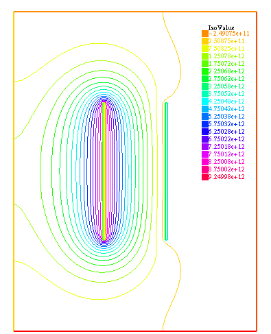
An example solution with the length of the layer (ie. the separation, ) being 20 µm and the thickness 2.7 µm is shown in Fig. 6. This calculation was done using the Freefem++ finite element solving software.freefem The ends are the contacts with on the left and on the right. The current crossing the top and bottom boundaries is set to zero, . The resulting current is uniform in the thickness but decreases from left to right due to the hole recombination a rate set by .
Surface recombination at the top and bottom interfaces can be simulated using sze2
| (5) |
where is the surface recombination velocity. Then the line integral in Eq. I.2.1 for the top boundary becomes
| (6) |
In this case some of the current stream lines bend into the top boundary and is no longer uniform in the thickness but is lower at the boundary. An example of Freefem++ code, “hole-diff-recom-vel-02.edp”, is included at the end of this appendix. Solving this using both surface recombination and bulk recombination give results that are consistent with using a single effective hole life time (and diffusion length). Our experiment cannot separate the two effects. It should be possible to determine the bulk and surface recombination life times using samples with different InGaAs layer thicknesses.
I.2.2 Edge effects of the contacts
The assumption made in the analytic solution of the 1d diffusion equation is that the entire current at the collecting electrode is collected at the leading edge of the contact. A finite element calculation (hole-diff-07-50.edp) of the hole current at a collecting contact on the top surface is given in Fig. 7. The largest current density is at the leading edge being about mAcm-2. Within 1 µm inside the edge the current density has dropped more than an order of magnitude to mAcm-2 and after 2 µm it has dropped to close to zero. This implies that the position to be used as the boundary for the 1d problem is between 1 and 2 µm in from the edge of the contact.
The analytic 1d model for a single type of hole is given by Eq. 1, which is repeated here
| (7) |
where is the distance between the injecting and collecting contacts, is the diffusion constant, is the diffusion length, and is the contact area. The geometry of the finite element version of the 1d model is shown in Fig. 8a (the same as Fig. 6). The left end of the rectangle is the injecting contact and the right end is the collecting contact. The current at the right end calculated by Freefem++ is exactly the same as the current found using Eq. 7, which confirms the finite element calculation.
a)
b)
c)
In order to investigate the effect of one top contact, the collecting electrode is added as a 10 µm segment on the top edge of the finite element model, which is shown in Fig. 8b. (Example Freefem++ code, “hole-diff-07-50.edp”, is added at the end of this appendix.) With this geometry the finite element calculation is less accurate due to current crowding and the change in flow direction at the leading edge of the collecting contact. Here the hole concentration changes rapidly causing some numerical inaccuracy which is magnified due to the current calculation using the derivative of the concentration. To investigate this, the current is found at a vertical line which is 1 µm in front of the edge of the collecting contact. This should be very close to the collecting contact current, only slightly higher since there will be a small amount of recombination after the vertical line. For some value of , using an inter diode separation of µm in the finite element model, the current calculated for this collecting contact is A (at the top contact) or A (at the vertical line). The correct value is in between these. This is slightly smaller than the current in the 1d model for , which is A. However, the 1d model for µm gives a current of A. This current matches the finite element result for the top collecting contact, which implies a correction to the length of 50 µm of 1.2 µm should be used in 1d model. The same calculations for µm gives the same value for the correction. The correction is only due to the distribution of the hole concentration near the contact and not affected by the separation between injection and collection (for the layer thickness).
The next step is to add a more realistic injecting contact on the top surface of the InGaAs layer as shown in Fig. 8c. The separation between the right edge of the injecting contact and the left edge of the collecting contact on the right hand side is 50 µm. The finite element calculated current at the collecting contact is A and A at the vertical line. This, again, is smaller than the 1d value for of A. To match the finite element 2d result one needs to use which gives A. Then the correction for to account for both contacts is about µm, which is twice the value that was found for only the collecting contact in the above.
I.2.3 Discussion about the edge correction
There are a couple of intuitive methods to check on the value of the end correction.
One is to assume that the best fit to the measured data will occur when using the correct value for . We have found that the fitting error given by the least squares routine is smallest for . This is consistent with the estimate given above by the finite element calculations.
The other method comes from considering that the relative error in the value of the separation, , is largest for the shortest separation distance, ie. in our case for µm. One can fit the data using all the data points and then again using all the data points excluding the first point. With the correct value of , the results of both fits should give the same values for and (see Eq. 10). The best value of can be found by trial and error. The results varry somewhat for different data sets. By this method we also find that , which is, again, cosistent with the above.
I.3 Diffusion of holes in the x-y plane
Since the length of the line diodes is finite, the holes will diffuse into the region beyond the diode ends. One might expect that some current would be lost due to hole recombination in this outer region. This diffusion in the plane can be modeled with a 2d finite element model, assuming that the InGaAs layer is negligibly thin and that all holes are emitted or collected exactly at the edges of the line diodes. Holes are injected by one line diode and diffuse away from it and are collected by a second line diode. This implies that the holes are confined to a thin layer in the direction and the concentration is uniform in that direction. The diffusion equation with recombination is
| (8) |
where , is the diffusion length. is the density of hole as a function of and , is the equilibrium hole density, is the hole life time, and D is the hole diffusion constant.
To solve this using the finite element method, the differential equation must be written in the weak (or integral) form,
| (9) |
The outer boundary of the area, , being simulated is assumed to have zero perpendicular current, so the line integral on the boundary is zero. The two line diodes are defined by rectangular boundaries inside the large rectangle as shown in Fig. 9. The boundary condition for the left hand, injecting, diode is the injected hole density, , and for the right side, collecting diode the boundary is set to the equilibrium hole density, . The solutions were calculated using the Freefem++ finite element solving software.freefem An example Freefem++ input file, two-hole-diff-01v.edp, is included at the end of this appendix.
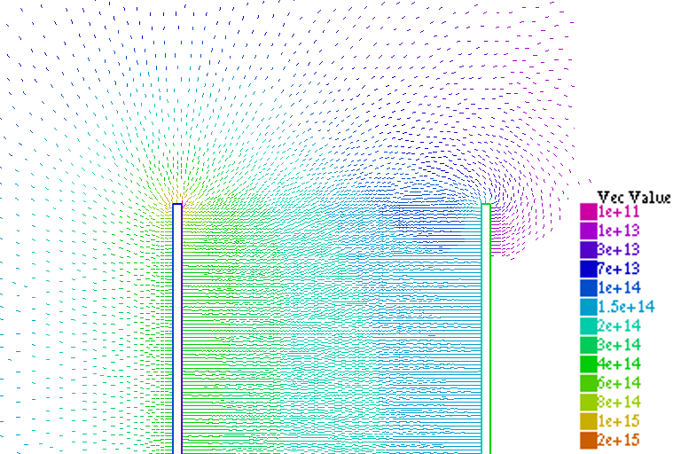
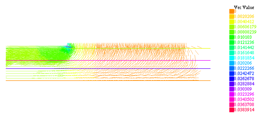
Current stream lines can be calculated from the derivatives of the hole concentration. These are drawn in Fig. 10. Current flows from all surfaces of the injecting diode, expands above the region between the diodes so that some current flows to the top and bottom ends and even around to the back of the collecting diode. This results in collected current being slightly larger than that predicted by the pure 1d formula. This is true except for small values of relative to , where a large fraction of holes are lost to recombination in the area outside the ends of the line diodes.
I.3.1 Numerical comparison of 2d and 1d current results
Collected current can be calculated for both the 2d and 1d methods in order to estimate the error made by using the 1d model due to end effects (which are included in the 2d finite element calculation). For these calculations the outer boundary of the finite element area was doubled compared to that shown in Fig. 9 such that the boundary is more than a few diffusion lengths away from the line diodes. Some results are presented in Table 1. For separations of 20 and 100 µm, the 1d model underestimates the actual current as calculated by the 2d model. The underestimation is larger as the diffusion length increases. This is due to the holes being able to diffuse further in the region above (and below) the ends of the line diodes. The case for µm and µm, the opposite occurs, that is the 1d model gives a larger current than the 2d model. This is due to more of the holes that diffuse into the regions above and below the ends of the line diodes being lost to recombination before they reach the collecting diode. In general, the relative error varies from less than 1% to as much as 7%. The effect this has on analyzing the experimental results in investigated in the next section.
| Separation | Model | µm | µm | µm |
|---|---|---|---|---|
| 20 µm | ||||
| 100 µm | ||||
| 330 µm |
I.3.2 Comparison with current measurements
Since the 2d calculation is more realistic (and so more accurate) than the 1d theory, ideally, one would fit the measured data the the 2d model. This would have to be done by trial and error guessing test values for the four fitting values and doing many repeated finite element calculations. This would be onerous compared to using the analytic 1d theory with which can use available non-linear least square fitting routines. In this section, fits to the 1d and 2d models will be compared and an improved result from the 2d model is obtained.
The finite element and 1d results will be compared using values found in the analysis of experimentally measured results. To do this, the finite element solution can be found separately for heavy and light holes with the collected current being the sum of both contributions. An example Freefem++ input file, two-hole-diff-01v.edp, is included at the end of this appendix. This can be compared to results of the 1d solution which is
| (10) |
where the and the subscripts refer to heavy or light hole values.
Results for a device from a different wafer (with an InGaAs layer doping level of ) than the results presented in the main APL paper, analyzed in the same way using the 1d theory with µm are plotted in Fig. 11, which shows similar results as those in Fig. 4 of the APL article.
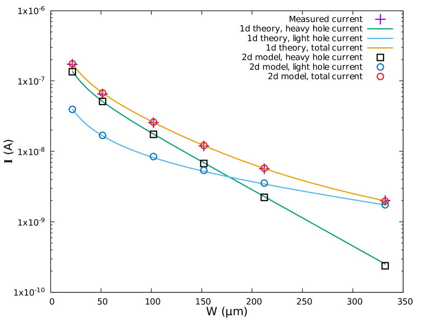
As an example, calculations are done for the case of an applied voltage of 0.3 V. The fit of the 1d theory, Eq. (10), to experiment gave , , , and . (Plotted in Fig. 11 for . These values are used in the finite element model to calculate the collected current for various values of separation. The outer boundaries in the finite element problem were expanded to be twice the size as that shown in Fig. 9 (1000 µm beyond the ends of the line diodes) in order for the boundary to be more than 3 diffusion lengths from the line diodes. The measured and the 2d calculated currents are in good agreement on the scale of the plot in Fig. 12. However, looking at the actual numbers, the 2d calculated currents are all slightly larger than the measured values (on the order of 1%), with the values at µm being closest to each other. The 2d model with the above values of and is not an optimal fit to the measured data. Then the calculated 2d current was fit to the 1d equation. This results in values µm µm, µm and µm. These are slightly different than the input values used to calculate the 2d current. The new and are 0.6% and 3.8% smaller and and are 1.6% and 2.5% larger, respectively. The 1d theory is plotted with these values in Fig. 12. Also plotted in Fig. 12 are the 2d calculated heavy and light hole currents compared to the 1d fit values of these. They are in good but not exact agreement, showing that the 1d model is a reasonable approximation to the 2d calculations.
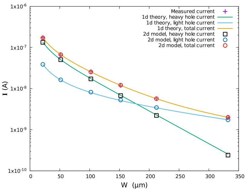
In order to achieve an improved fit of the 2d FE model to the measured data, a second iteration of the finite element calculation was done. The above two sets of and values were used as a guide to give improved values to use in the finite element calculation. These improved input values are µm, µm, µm, and µm. The new 2d current calculated values are plotted in Fig. 13. While this looks identical to Fig. 12, it is reproduced here to demonstrate how close the two results are. Again the total finite element currents match the measured values on the scale the plot. Looking at the actual numbers, the 2d calculation is now a very good fit to the data. The quality of this fit is similar to the original fit of the 1d theory to the data, so the fitting uncertainties would imply that the 2d and 1d models are equally good. If, due to the physics, one considers the 2d FE model to be more realistic than the 1d theory, then the new values for and used in the second finite element calculation are improved values for the actual sample. Also plotted are the 1d currents from the fit of Eq. 10 to the new finite element calculated values. These new 1d fit values are similar to the original values from the fit of the 1d theory to the measured currents, but they have smaller fitting errors. This fitting error is due to the difference between the 2d model and the 1d model. It does not represent the experimental measurement errors.
The above improved result plus the similarly calculated improved result for are plotted in Fig. 11. The difference between the 2d analysis and the 1d analysis is small, well within the uncertainties for this experiment, so using the 1d theory to analyze the data is satisfactory.
As was shown above corrections to the 1d theory due both to the transfer length at the edge of the contacts () and diffusion in the plane at the line ends were small, about 1%. However, since the fit is using 4 parameters, the fit results are sensitive to these small corrections. The experimental errors in our measurements mask these small corrections, but with a more accurate measurement of the currents, the 2d corrections may be more important.
I.3.3 Note on the fitting method
In this appendix, the fits of the 1d theory to the current measurements were done using the nonlinear least-squares Marquardt-Levenberg algorithm in gnuplot. gnuplot In order to give similar weight to all data points, the logarithm of the measured currents was fit to the logarithm of Eq. 10. Due to the relatively large number (4) of fitting parameters and the fact that the logarithm of current plotted against does not deviate too much from a straight line, the fitting is difficult. The result is that small experimental errors in the current points leads to large uncertainty in the resulting fit. In a few cases, the fitting algorithm could not find a stable result. This means that the fits had to be monitored manually to insure reasonable results.
Compounding the above is that the 1d theory does not exactly represent the actual 3d device (as was shown in previous sections). This means there will be some fitting error even in the ideal case of no experimental current measurement errors.
I.4 Low injection assumption
As well as the 1d assumption, we also use the assumption of low injection. In this case the minority hole concentration must be much less than the electron concentration. In the case of medium injection, the injected hole density will be somewhat lower than the prediction of the formula used for low injection.cristea In our case the decrease in injected hole concentration would be about 1% at a junction voltage of 0.37 V. Low injection also allows us to assume that the electric field is zero in the neutral region, so that the current is only due to diffusion. It also implies that the electron concentration is unperturbed so that electrons do not contribute to the current. The medium injection current is discussed in some detail by Kasap and Tannous,kasap who give some ways to calculate when these effects become important.
A second consequence of the move away from small injection and the existence of an electric field in the neutral region is that the whole of the applied voltage is no longer across the diode junction. In our case, the current from the injecting diode to the ground must cross the bottom heterojunction and there could be a potential drop there. In addition other sources of series resistance, such as contact resistance, will also lower the junction voltage as current gets larger. This affects the calculation of the hole concentration under the injecting junction. Above low injection, our calculation of will be too high. This correction of the diode potential will lead to a lower , which does not affect the value of , but it does affect the determined values of (or mobility) and . Since our device structure is quite complicated, an attempt to calculate the voltage correction will not be done. However, in our experiments, the curves drop below the ideal exponential dependence by about 1% at about V, indicating the beginning of the aforementioned effects.
I.5 Band parameters
Values for the electron and hole effective masses and the band gap have been assumed. These values are used in the calculation of and . This directly effects the values of (or ) and , but it does not effect the value of . This can be seen by writing Eq. 10 as , where and are constants. The effective masses are not well known, with values found in the literature varying by 10 to 20%. This means the determination of (or ) and have this same uncertainty.
Another point is that and
are strongly dependent on temperature, , so
that the sample temperature must be accurately measured.
I.6 Future
Finally, a few possible extensions of the above experiment will be mentioned, without any attempt to work out the details.
Another way to improve the experiment would be to measure some of the parameters independently. For example, if experiment or theory could fix the ratio of the life times (in the simplest case, ), then there would be only three independent fitting parameters. This greatly reduces the rms fitting errors. It may also be possible to measure the life times on the same devices using time dependent measurements. The and would be known and the only fitting parameters would be and , again leading to better fitting results.
A mesa etch of the whole set of line diode devices would stop current spreading beyond the ends of the line diodes in the plane. A simple analysis would require that there was no recombination on the etched sidewalls.
Acknowledgment
The electrical measurements were done by Alexandre Walker. The method of analysis was jointly developed by Alexandre Walker and Mike Denhoff.
References
- (1) J. N. Reddy, An Introduction to the Finite Element Method, 3rd ed., McGraw Hill, New York, 2006.
- (2) F. Hecht, Freefem++, 3rd ed., [freefem++doc.pdf], version 3.18, 2012. Available: http://www.freefem.org/ff++. The calculations were made using FreeFem++ version 3.47.
- (3) S. M. Sze, Physics of Semiconductor Devices, 3rd ed., Wiley: New York, 2007.
- (4) gnuplot 5.0, Interactive Plotting Program. Web access: http://sourceforge.net/projects/gnuplot
- (5) M. J. Cristea, “Unified model for p-n junction current-voltage characteristics”, arXiv:0907.1383 (2009), https://arxiv.org.
- (6) S.O. Kasap and C. Tannous, “The Pedagogy of the p-n Junction: Diffusion or Drift?”, (2003), https://arxiv.org/abs/physics/0306153.
I.7 Example code
The following examples of Freefem++ input code were developed until they barely worked. They have not been carefully tested or optimized for correctness or accuracy.
I.7.1 hole-diff-recom-vel-02.edp
The following is an example input file to Freefem++ which was used to calculate Fig. 6 (with Sp = 0.0).
I.7.2 hole-diff-07-50.edp
The following Freefem++ file was used to generate Fig.8b and calculate the current for this case.
I.7.3 two-hole-diff-01v.edp
This Freefem++ file was used to calculate the results in Fig. 12.