Proximity-induced superconductivity within the InAs/GaSb edge conducting state.
Abstract
We experimentally investigate Andreev transport through the interface between an indium superconductor and the edge of the InAs/GaSb bilayer. To cover all possible regimes of InAs/GaSb spectrum, we study samples with 10-nm, 12 nm, and 14 nm thick InAs quantum wells. For the trivial case of a direct band insulator in 10 nm samples, differential resistance demonstrates standard Andreev reflection. For InAs/GaSb structures with band inversion (12 nm and 14 nm samples), we observe distinct low-energy structures, which we regard as direct evidence for the proximity-induced superconductivity within the current-carrying edge state. For 14 nm InAs well samples, we additionally observe mesoscopic-like resistance fluctuations, which are subjected to threshold suppression in low magnetic fields.
pacs:
73.40.Qv 71.30.+hI Introduction
Similarly to HgTe quantum wells konig ; kvon , InAs/GaSb bilayers can demonstrate inverted energy spectra hughes08 . For a typical value of 10 nm for the GaSb layer, InAs/GaSb structures with 12 nm thick InAs wells are usually regarded as topological insulators hughes08 ; gasb2 ; gasb4 ; nowack14 ; gasb6 ; suzuki . Thinner (10 nm) or thicker (14 nm) InAs wells correspond suzuki ; tiemann to a direct band semiconductor or an indirect band two-dimensional semimetal, respectively. InAs/GaSb bilayers posses many advantages over HgTe quantum wells, including better stability, much easier III-V materials processing and spectra tunability by front and back gates hughes08 . However, there is residual bulk conductivity in InAs/GaSb structures, which complicates experimental investigation of edge transport suzuki ; knez15 .
Topological edge states with spin-momentum locking are expected for structures with band inversion zhang1 ; kane ; zhang2 ; ando . Current-carrying edge states were demonstrated for InAs/GaSb bilayers in transport experiments suzuki ; knez15 ; nowack14 ; pribiag15 ; nichele16 , although their topological nature is still debatable nichele16 .
Edge state transport is of special interest for regions with proximity-induced superconductivity Fu ; yakoby ; beenakker13 , because of a search for Majorana fermions with non-Abelian statistics reviews and prospects for quantum computing beenakker13 ; kitaev . This activity requires detailed investigation of Andreev transport in systems with non-trivial energy spectra adroguer ; visani ; finck .
Andreev reflection andreev allows charge transport from normal metal (N) to superconductor (S) at energies below the superconducting gap. An electron is injected through the NS interface by creating a Cooper pair, so a hole is reflected back to the N side of the junction andreev ; tinkham . Usually, Andreev reflection is not sensitive to the details of band structure in the normal lead tinkham . However, for graphene or semimetal spectra, the reflected hole can appear in the valence band, which is known as specular (or interband) Andreev reflection been1 ; been2 ; spec . Also, an additional energy scale appears if Andreev transport goes through an intermediate conductive region, which is partially decoupled from the bulk normal conductor heslinga ; klapwijk17 .
Here, we experimentally investigate Andreev transport through the interface between an indium superconductor and the edge of the InAs/GaSb bilayer. To cover all possible regimes of InAs/GaSb spectrum, we study samples with 10-nm, 12 nm, and 14 nm thick InAs quantum wells. For the trivial case of a direct band insulator in 10 nm samples, differential resistance demonstrates standard Andreev reflection. For InAs/GaSb structures with band inversion (12 nm and 14 nm samples), we observe distinct low-energy structures, which we regard as direct evidence for the proximity-induced superconductivity within the current-carrying edge state. For 14 nm InAs well samples, we additionally observe mesoscopic-like resistance fluctuations, which are subjected to threshold suppression in low magnetic fields.
II Samples and technique
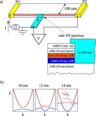
Our samples are grown by solid source molecular beam epitaxy on semi-insulating GaAs (100) substrate. The InAs/GaSb double quantum well is sandwiched between two 50 nm thick AlSb barriers. Details on the growth parameters can be found elsewhere growth . To cover all possible regimes of the InAs/GaSb bilayer spectrum suzuki ; tiemann , we prepare samples with a 10-nm thick GaSb quantum well and different, 10-nm, 12 nm, and 14 nm thick InAs ones, see Fig. 1.
As obtained from standard magnetoresistance measurements, the 10 nm and 14 nm samples are characterized by bulk electron-type conductivity, while it is hole-type for the 12 nm ones. The low-temperature mobility is found to be one order of magnitude higher for bulk electrons ( cm2/Vs) than for holes ( cm2/Vs). These values are in good correspondence with known ones for InAs/GaSb double quantum wells hughes08 ; gasb2 ; gasb4 ; nowack14 ; gasb6 , taking into account low bulk carrier concentration, which is roughly cm-2 in all our samples.
A sample sketch is presented in Fig. 1 (a). The nm high mesa is formed by wet chemical etching down to the bottom GaSb layer. Since the edge effects are of prime interest in InAs/GaSb bilayers hughes08 ; gasb2 ; gasb4 ; nowack14 ; gasb6 , side nbsemi ; nbhgte superconducting contacts are made at the mesa step. They are formed from thermally evaporated 100 nm thick indium film by lift-off with low (1-2 m) mesa overlap, see Fig. 1 (a). Because of the insulating top AlSb barrier, vertical transport is forbidden in the overlap region. We take special care to obtain equally prepared In–InAs/GaSb interfaces. Both the processing steps, wet etching and indium evaporation, are made simultaneously for samples with 10-nm, 12 nm, and 14 nm thick InAs quantum wells. Ohmic contacts are made by thermal evaporation of 100 nm Au film with few nm Ni to improve adhesion.
We study charge transport across a single NS junction between the indium side contact and the InAs/GaSb mesa edge in a standard three-point technique, see Fig. 1 (a): the superconducting electrode is grounded; a current (-2 to +2 A range) is fed to InAs/GaSb bilayer through one of the normal Ohmic contacts, N1 in Fig. 1; the other normal contact (N2, respectively) traces the potential .
To obtain characteristics, the current is additionally modulated by a low ac (20 pA, 110 Hz) component. We measure both, dc () and ac (), components of the potential by using a dc voltmeter and a lock-in, respectively. We check, that the lock-in signal is independent of the modulation frequency in the 60 Hz – 300 Hz range, which is defined by applied ac filters. To extract features specific to the InAs/GaSb bilayer system, the measurements are performed at 30 mK. Similar results are obtained from different samples in several cooling cycles.
III Experimental results
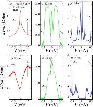
Fig. 2 demonstrates examples of curves for samples with different thickness of InAs quantum well. In a three-point technique, the measured potential reflects in-series connected resistances of the grounded contact and some part of the 2D system. In our experiment the former term is dominant, because of highly resistive junctions, see Fig. 2. The indium lead is superconducting, so characteristics reflect charge transport through a single (grounded) NS interface. To support this conclusion experimentally, the obtained characteristics are verified to be independent of the exact positions of current and voltage probes.
Despite of equally prepared In–InAs/GaSb interfaces, curves demonstrate even qualitative different behavior in samples with different thickness of InAs quantum well in Fig. 2. Since the curves of NS junctions are known to be highly sensitive to the interface potential fluctuations BTK , the top and the bottom panels in Fig. 2 demonstrate maximum device-to-device fluctuations for a given InAs quantum well thickness.
The 10 nm wide InAs quantum well sample demonstrates a typical example of Andreev reflection at the disordered NS interface tinkham , see Fig. 2 (a-b). In (a), the differential resistance is increased within the indium superconducting gap meV to about , so single-particle scattering is significant at the interface BTK . In Fig. 2 (b), there is a resistance drop within meV, as it is expected for cleaner NS interface andreev ; BTK . There is no any additional features for the curves in Fig. 2 (a-b), as it should be anticipated for standard Andreev reflection.

In Fig. 2 (c-d), the subgap resistance is about kOhm in different samples at meV. It is much higher than the normal value kOhm for . Which is specific for the 12 nm samples, there is always well-developed peak within mV bias.
The behavior is even more complicated for the 14 nm samples, see Fig. 2 (e-f). Differential resistance demonstrates sharp peaks at , the subgap and normal values are comparable with the 10 nm case. However, a zero-bias resistance dip appears in Fig. 2 (e-f), which is accompanied by a number of additional resistance peaks of different amplitude. They are well reproducible for a given sample and symmetric in respect to the bias sign.
First of all, we demonstrate that the presented in Fig. 2 curves are connected with superconductivity. Fig. 3 (a) demonstrates that the superconductivity can be completely suppressed above , which well corresponds to the known indium bulk indium critical filed. We fix the zero bias and sweep the magnetic field slowly. The resistance drop is sharp at 30 mK (as shown for the 12 nm sample), while temperature broadening is demonstrated at 1.2 K for the 10 nm sample in Fig. 3. To avoid orbital effects, the field is oriented within the bilayer plane (with accuracy) along the mesa edge, so it is strictly in-plane oriented also for the superconducting film at the mesa step. We obtain similar results for the normally oriented magnetic field. Monotonous suppression is fully consistent with the classical Andreev reflection picture tinkham .
Fig. 3 (b) demonstrates specifics of the low-field behavior for the 14 nm samples. One can see strong mesoscopic-like fluctuations within interval, which are completely suppressed at higher fields.
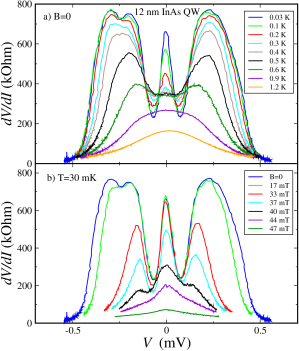
Fig. 4 demonstrates detailed behavior with temperature or magnetic field increase for the 12 nm sample. The resistance peak within mV is well visible for temperatures below K, see Fig. 4 (a), and for magnetic fields below 40 mT in Fig. 4 (b). At the temperature of , curve is still nonlinear because of much higher indium . The superconductivity is gradually suppressed above 30 mT in Fig. 4 (b), further increase of magnetic field results in a nearly flat curve even at lowest mK.
IV Discussion
Within the classical framework of Andreev reflection tinkham , it is not sensitive to details of band structure in a normal lead. However, even qualitative effect on can be seen in Fig. 2 for samples with different InAs quantum well widths. Because the observed subgap features are independent of the maximum device-to-device fluctuations, we have to attribute them to different edge properties of our InAs/GaSb structures, which are defined by bulk spectrum hughes08 ; gasb2 ; gasb4 ; nowack14 ; gasb6 .
No edge specifics can be expected for a trivial insulator in 10 nm thick InAs quantum well samples. Monotonous curves in Fig. 2 (a-b) do not demonstrate subgap features, they are only sensitive to the disorder at the interface BTK .
In the case of 12 nm thick InAs quantum well, the current-carrying edge states appear, because of the inverted band structure. This statement seems to be firmly confirmed by experiments hughes08 ; gasb2 ; gasb4 ; nowack14 ; gasb6 . Moreover, the edge current was directly demonstrated in visualization experiments nowack14 ; imaging to coexist with finite bulk conductivity, most likely due to the edge depletion region. The latter leads to strongly increased differential resistance in Fig. 2 (c-d). The proximity-induced superconducting gap can be expected within the edge state near the indium superconducting lead adroguer .
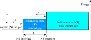
Andreev transport through the intermediate conductive region has been regarded both experimentally heslinga ; klapwijk17 and theoretically akhmerov17 . In a crude qualitative picture, see Fig. 5, the NS’ interface with the region of induced superconductivity S’ is responsible for Andreev reflection at biases below the induced gap , while above this value the NS interface with bulk superconductor governs the reflection process. Because of different single-particle transparency of two interfaces, contains heslinga ; klapwijk17 an additional structure at low biases. The induced gap can be estimated from the width of this structure heslinga ; klapwijk17 in Fig. 2 (c-d) as meV.
Because the edge conductive region is of finite width nowack14 ; imaging , the induced gap should be defined by Thouless energy (see Appendix to Ref. akhmerov17, for recent comprehensive discussion). This statement is in qualitative agreement with our experiment: (i) as expected golubov15 for , the width of the low-bias structure is constant in Fig. 4 (a), until exceeds at 0.9 K; (ii) also, is insensitive golubov15 to partial suppression of the bulk superconducting gap by magnetic field, as we observe in Fig. 4 (b). As for numerical estimations, in the regime of diffusive transport. If we use the bulk values, and nm, we can estimate as 60 nm from the experimental value of meV. This crude estimation corresponds well to the experimentally obtained pribiag15 value nm.
Because of the band inversion, we can also expect tiemann the edge conductive region for samples with 14 nm width of the InAs quantum well. Thus, the zero-bias resistance dip in Fig. 2 (e-f) can also be regarded as the induced gap . However, the subgap resistance peaks in Fig. 2 (e-f) and mesoscopic-like fluctuations in low fields in Fig. 3 (b) resemble modulation akhmerov17 ; chevallier of density of states due to the quasiparticle interference akhmerov17 . It appears adroguer ; tomasch1 for ballistic transport, which seems to be reasonable for nm in the 14 nm samples. In this case, the threshold suppression of the mesoscopic-like fluctuations reflects the interference breakdown in magnetic field. It is important, that we do not observe any subgap features for the 10 nm samples with the similar nm value, where no edge conductive region can be expected. Thus, we can regard the subgap resistance features in Fig. 2 (c-d) and (e-f) as a direct evidence for the proximity-induced superconductivity within the current-carrying edge states in InAs/GaSb structures with band inversion.
V Conclusion
As a conclusion, we experimentally investigate Andreev transport through the interface between an indium superconductor and the edge of the InAs/GaSb bilayer. To cover all possible regimes of InAs/GaSb spectrum, we study samples with 10-nm, 12 nm, and 14 nm thick InAs quantum wells. For the trivial case of a direct band insulator in 10 nm samples, differential resistance demonstrates standard Andreev reflection. For InAs/GaSb structures with band inversion (12 nm and 14 nm samples), we observe distinct low-energy structures, which we regard as direct evidence for the proximity-induced superconductivity within the current-carrying edge state. For 14 nm InAs well samples, we additionally observe mesoscopic-like resistance fluctuations, which are subjected to threshold suppression in low magnetic fields.
Acknowledgements.
We wish to thank Ya. Fominov, D.E. Feldman, V.T. Dolgopolov, and T.M. Klapwijk for fruitful discussions. We gratefully acknowledge financial support by the RFBR (project No. 16-02-00405) and RAS.References
- (1) M. König, S. Wiedmann, C. Brüne, A. Roth, H. Buhmann, L. W. Molenkamp, X.-L. Qi, and S.-C. Zhang, Science 318, 766 (2007).
- (2) G. M. Gusev, Z. D. Kvon, O. A. Shegai et al. , Phys. Rev. B 84, 121302(R) (2011).
- (3) C. Liu, T.L. Hughes, X.-L. Qi, K. Wang, and S.-C. Zhang, Phys. Rev. Lett. 100, 236601 (2008).
- (4) I. Knez, R.-R. Du, and G. Sullivan, Phys. Rev. Lett. 107, 136603 (2011).
- (5) I. Knez, C. T. Rettner, S.-H. Yang, S. S. P. Parkin, L. Du, R.-R. Du, and G. Sullivan, Phys. Rev. Lett. 112, 026602 (2014).
- (6) E.M. Spanton, K.C. Nowack, L. Du, G. Sullivan, R.-R. Du, K.A. Moler, Phys. Rev. Lett. 113, 026804 (2014).
- (7) L. Du, I. Knez, G. Sullivan, and R.-R. Du, Phys. Rev. Lett. 114, 096802 (2015).
- (8) K. Suzuki, Y. Harada, K. Onomitsu, and K. Muraki, Phys. Rev. B 87, 235311 (2013).
- (9) L. Tiemann, S. Mueller, Q.-S. Wu, T. Tschirky, K. Ensslin, W. Wegscheider, M. Troyer, A.A. Soluyanov, and T. Ihn, Phys. Rev. B 95, 115108 (2017).
- (10) L. Du, I. Knez, G. Sullivan, R.-R. Du, Phys. Rev. Lett. 114, 096802 (2015).
- (11) S. Murakami, N. Nagaosa, S.-C. Zhang, Phys. Rev. Lett. 93, 156804 (2004).
- (12) C. L. Kane, E. J. Mele, Phys. Rev. Lett. 95, 146802 (2005).
- (13) B. A. Bernevig, S.-C. Zhang, Phys. Rev. Lett. 96, 106802 (2006).
- (14) Y. Ando, J. Phys. Soc. Jpn. 82, 102001 (2013).
- (15) V.S. Pribiag, A.J.A. Beukman, F. Qu, M.C. Cassidy, C. Charpentier, W. Wegscheider and L.P. Kouwenhoven, Nature Nanotechnology 10, 593–597 (2015).
- (16) F. Nichele, H.J. Suominen, M. Kjaergaard, C.M. Marcus, E. Sajadi, J.A. Folk, F. Qu, A.J.A. Beukman, F.K. de Vries, J. van Veen, S. Nadj-Perge, L.P. Kouwenhoven, B.-M. Nguyen, A.A. Kiselev, W. Yi, M. Sokolich, M.J. Manfra, E.M. Spanton and K.A. Moler, New J. Phys. 18, 083005 (2016).
- (17) L. Fu and C. L. Kane, Phys. Rev. Lett. 100, 96407 (2008).
- (18) S. Hart, H. Ren, T. Wagner, Ph. Leubner, M. Mühlbauer, C. Brüne, H. Buhmann, L. W. Molenkamp and A. Yacoby, Nature Physics 10, 638–643 (2014).
- (19) C.W.J. Beenakker, Annu. Rev. Con. Mat. Phys. 4, 113 (2013).
- (20) For recent reviews, see C. W. J. Beenakker, Annu. Rev. Con. Mat. Phys. 4, 113 (2013) and J. Alicea, Rep. Prog. Phys. 75, 076501 (2012).
- (21) S.B. Bravyi and A.Y. Kitaev, Annals of Physics 298, 210 (2002).
- (22) P. Adroguer, C. Grenier, D. Carpentier, J. Cayssol, P. Degiovanni, and E. Orignac, Phys. Rev. B 82, 081303(R), (2010).
- (23) C. Visani, Z. Sefrioui, J. Tornos, C. Leon, J. Briatico, M. Bibes, A. Barth´el´emy, J. Santamara and Javier E. Villegas, Nature Physics, 8, 539 (2012).
- (24) A.D.K. Finck, C. Kurter, Y.S. Hor, D.J. Van Harlingen, Phys. Rev. X 4, 041022 (2014).
- (25) A. F. Andreev, Soviet Physics JETP 19, 1228 (1964).
- (26) M. Tinkham, Introduction to Superconductivity (2d ed., McGraw–Hill, New York, 1996).
- (27) C. W. J. Beenakker, Physical Review Letters 97 (2006).
- (28) C. W. J. Beenakker, Reviews of Modern Physics 80, 1337 (2008).
- (29) Wei Chen, Liang Jiang, R. Shen, L. Sheng, B. G. Wang, D. Y. Xing EPL 103, 27006 (2013)
- (30) D.R. Heslinga, S.E. Shafranjuk, H. van Kempen, and T.M. Klapwijk, Phys. Rev. B 49, 10484 (1994).
- (31) J. Wiedenmann, E. Liebhaber, J.s Kübert, E. Bocquillon, Ch. Ames, H. Buhmann, T.M. Klapwijk, L.W. Molenkamp, arXiv:1706.01638.
- (32) E.A. Emel’yanov, D.F. Feklin, A.V. Vasev, M.A. Putyato, B.R. Semyagin, A.P. Vasilenko, O.P. Pchelyakov, V.V. Preobrazhenskii, Optoelectronics, Instrumentation and Data Processing, 47, 452 (2011).
- (33) A. Kononov, S. V. Egorov, Z. D. Kvon, N. N. Mikhailov, S. A. Dvoretsky, and E. V. Deviatov, Phys. Rev. B 93, 041303(R) (2016)
- (34) A. Kononov, S. V. Egorov, N. Titova, Z. D. Kvon, N. N. Mikhailov, S. A. Dvoretsky, E. V. Deviatov, JETP Lett., 101 , 41 (2015).
- (35) G.E. Blonder, M. Tinkham, T.M. Klapwijk, Physical Review B, 25, 4515 (1982).
- (36) A. M. Toxen Phys. Rev. 123, 442 (1961)
- (37) K.C. Nowack, E.M. Spanton, M. Baenninger, et al., Nature Materials 12, 787 (2013).
- (38) T.Ö. Rosdahl, A. Vuik, M. Kjaergaard, A.R. Akhmerov, arXiv:1706.08888v1.
- (39) M. Snelder, M.P. Stehno, A.A. Golubov, C.G. Molenaar, T. Scholten, D. Wu, Y.K. Huang, W.G. van der Wiel, M.S. Golden, and A. Brinkman, arXiv:1506.05923.
- (40) D.I. Pikulin and T. Hyart, Phys. Rev. Lett. 112, 176403 (2014).
- (41) D. Chevallier, P. Simon, and C. Bena, Phys. Rev. B 88, 165401 (2013).
- (42) W. J. Tomasch, Phys. Rev. Lett. 16, 16 (1966).