Survey of the class of isovalent antiperovskite alkaline earth-pnictide compounds
Abstract
The few reported members of the antiperovskite structure class of alkaline earth ( = Ca,Sr,Ba) pnictides ( = N,P,As,Sb,Bi) compounds are all based on the B-site anion =N. All fit can be categorized as narrow gap semiconductors, making them of interest for several reasons. Because chemical reasoning suggests that more members of this class may be stable, we provide here a density functional theory (DFT) based survey of this entire class of compounds. We determine first the relative energetic stability of the distribution of pairs of ions in the A and B sites of the structure, finding that the site always favors the small pnictogen anion. The trends of the calculated energy gaps with cation and anions are determined, and we study effects of spin-orbit coupling as well as two types of gap corrections to the conventional DFT electronic spectrum. Because there have been suggestions that this class harbors topological insulating phases, we have given this possibility attention and found that energy gap corrections indicate the cubic structures will provide at most a few topological insulators. Structural instability is addressed by calculating phonon dispersion curves for a few compounds, with one outcome being that distorted structures should be investigated further for thermoelectric and topological character. Examples of the interplay between spin-orbit coupling and strain on the topological nature are provided. A case study of including the effect of strain illustrates how a topological semimetal can be transformed into topological insulator and Dirac semimetal.
I Introduction
Oxide-based perovskites are the most studied class of ternary compounds for several reasons. First, oxygen is abundant and a great deal is known about oxide chemistry. Second, the basic cubic structure ABO3 is simple and is governed to a great extent by ionic bonding. Third, given the near universal valence state , the and cation valences must total six, leaving a large number of combinations 1:5, 2:4, 3:3, 4:2, 5:1, considering the number of atoms that can assume these formal valences. Most importantly perhaps is the vast range of properties displayed by oxide perovskites, including high temperature superconductivity, much unusual magnetism, charge, spin, and orbital ordered phases, large linear responses (viz. Born effective charges that can differ by a factor of two or more from the formal charge), multiferroic states, among others.
Halide-based perovskites, viz. KMnF3 with a monovalent anion, are a closely related class of materials. They are much less prevalent because only 1:2 and 2:1 cation charge pairs are possible, and the higher eletronegativity makes synthesis less straightforward. Less common still are nitrogen based perovskites, because the ion requires cations with formal charge pairs 4:5 or 3:6; higher formal valences are rare. N-based perovskites have been the topic of a high-throughout computational study to determine stable examples.Perez2015
Within a given crystal structure it is uncommon, but possible, to interchange the anion and cation sites. The antiperovskite class discussed here will be denoted AB, where is the (alkaline earth) cation on the oxygen site and A and B are anions that provide charge balance. Anion formal valences are practically limited to 1, 2, and 3, constraining considerably the cation valences. In this paper we will focus on divalent alkaline earth cations, for which the anion formal charges must sum to six, so it can be expected that nearly all of such antiperovskite compounds will have two trivalent anions. Here we consider the class in which both A and B anions are from the pnictogen column of the period table. Given the formal charge balance between divalent cations and trivalent anions, this class can be anticipated to harbor insulators and perhaps semimetals. Sun and coauthors have proposed that topological insulating phases may arise in the BiN group with application of uniaxial strain,Sun2010 providing additional current interest.
Examples of alkaline earth-pnictide antiperovskite compounds have been reported. Some crystallize in cubic structure,chern1992a while others show structural distortionschern1992b or even form distinct structures, e.g. the two compounds Ba3(Sb,Bi)N assume the hexagonal antiperovskite structureniewa2013 , suggested to be due to the presence of large radii alkaline earth ions. The electronic state of this class of materials is insulating, ranging from relatively wide gap insulating to narrow gap semiconducting. The reported compounds will be discussed in Sec. III.4 in relation to our results. Notably, compounds in this class with pnictides other than N inside the octahedron have not been reported.
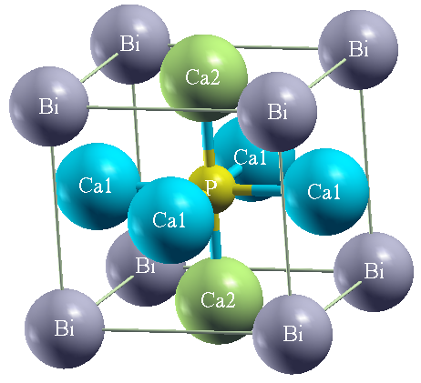
Density functional theory (DFT) based study of insulating Ca3BiN and metallic Ca3PbN provided the underlying electronic structure (as shown in the current paper) of this class of materials.papa1992 DFT based results for the band structure and selected properties (primarily bandgap, elastic, thermoelectric) have been reported for several of these compounds, which are discussed in Sec. III.4 below. Motivated by the relatively few known examples and the broad possibilities for new materials with important properties, we have carried out a survey on the entire class of alkaline earth-pnictide antiperovskite compounds, viz. , where and , using first principles DFT methods. The conventional ordering of atoms and will follow that of a perovskite with general chemical formula , where the cation is 12-fold cub-octahedral coordinated and is 6-fold coordinated by an octahedron of O anions. In the case of antiperovskite , is inside the octahedron while sits in the more open A site.
The manuscript is organized as follows. The computational methods are summarized is Sec. II. Section III contains much of the basic results, and includes a general analysis of the common features of these antiperovskites, the correction to DFT bandgaps that are important for small (or negative) gap compounds, and a synopsis of previously reported or predicted members of this class. The possibility of topological character, and the favorable candidates, are described Sec. IV. Section V addresses the question of structural stability with two examples, and a concise summary is given in Sec. VI.
II Computational Methods
To study the electronic structure of these 75 compounds, the generalized gradient approximation (GGA) exchange-correlation functional of Perdew-Burke-Ernzerhof-1996Perdew1996 was used, as implemented in the full-potential local orbital (FPLO) Koepernik1999 scheme. Self-consistency was obtained on a dense -mesh of to ensure good convergence of the density and thereby the eigenvalues. The fully relativistic Dirac four component equations implemented in FPLO were performed to include spin-orbit coupling and other relativistic corrections. The cubic lattice constants were obtained by minimizing the energy with respect to volume.
In small gap compounds, and especially for potential topological materials where gaps are typically quite small, the underestimate of the band gap by the GGA functional must be dealt with. We have calculated band gap corrections of the Bi subclass using the modified Becke-Johnson (mBJ) exchange-correlation potential. This scheme provides a self-energy-like correction to eigenvalues that has been found to be realistic for several semiconductors and insulators.Becke2006 ; Tran2007 ; Tran2009 A formally well justified means of obtaining self-energy corrections is provided by GW approximation.FHI-gap ; Jiang2016 We have used the FHI-gap implementationFHI-gap in the WIEN2K codeBlaha2001 on four compounds, and make comparison with the mBJ results in Sec. III.3. In this implementation the eigenvalue in is iterated to self-consistency, hence our use of the terminology throughout. The linearized augmented plane wave basis was specified by =7, where in the minimum radius of the atomic spheres and is the largest reciprocal lattice vector. For the version of implemented in FHI-gap, the mixed basis quality was determined by = 3, = 0.75. Unoccupied states up to 1000 eV were summed over, the number of discrete imaginary frequency points was 16, and the k-point mesh was . Increasing the latter to resulted in self-energy changes of the order of 0.01 eV.
III Analysis of Cubic Structures and Spin-Orbit Coupling
III.1 Cell volume and energetic stability
| NB | PB | AsB | SbB | BiB | ||||||||||||||||||||||
| NA | a(Å) | (eV) | (eV) | (eV) | a(Å) | (eV) | (eV) | (eV) | a(Å) | (eV) | (eV) | (eV) | a(Å) | (eV) | (eV) | (eV) | a(Å) | (eV) | (eV) | (eV) | ||||||
| Ca | 4.61 | - | 0. | 0. | 1 | 5.29 | - | SM | M | 1 | 5.42 | - | 0. | 0. | 1 | 5.76 | - | -0.01 | -0.02 | 1 | 5.85 | - | -0.01 | -0.04 | 1 | |
| Sr | 4.99 | - | 0. | 0. | 1 | 5.67 | - | 0. | 0. | 1 | 5.80 | - | 0. | -0.01 | 1 | 6.13 | - | -0.02 | -0.03 | 1 | 6.23 | - | -0.02 | -0.05 | 1 | |
| Ba | 5.33 | - | SM | SM | 1 | 6.03 | - | -0.04 | -0.05 | 1 | 6.18 | - | -0.05 | -0.06 | 1 | 6.52 | - | -0.07 | -0.08 | 1 | 6.61 | - | -0.05 | -0.12 | 1 | |
| PA | Ca | 4.73 | -2.96 | 0.85 | 0.85 | 0 | 5.31 | - | 0.33 | 0.31 | 0 | 5.42 | - | 0.10 | 0.05 | 0 | 5.74 | - | 0. | 0. | 1 | 5.82 | - | 0. | 0. | 1 |
| Sr | 5.09 | -2.55 | 0.45 | 0.45 | 0 | 5.67 | - | 0. | 0. | 1 | 5.79 | - | 0. | 0. | 1 | 6.09 | - | 0. | 0. | 1 | 6.17 | - | 0. | 0. | 1 | |
| Ba | 5.43 | -2.28 | SM | SM | 0 | 6.02 | - | 0.03 | 0.01 | 1 | 6.14 | - | 0. | 0. | 1 | 6.44 | - | 0. | 0. | 1 | 6.53 | - | 0. | -0.10 | 1 | |
| AsA | Ca | 4.78 | -3.38 | 0.77 | 0.72 | 0 | 5.34 | -0.55 | 0.15 | 0.09 | 0 | 5.45 | - | 0. | 0. | 1 | 5.75 | - | 0. | 0. | 1 | 5.84 | - | 0. | 0. | 1 |
| Sr | 5.13 | -2.93 | 0.30 | 0.28 | 0 | 5.70 | -0.50 | 0. | 0. | 1 | 5.81 | - | 0. | 0. | 1 | 6.11 | - | 0. | 0. | 1 | 6.19 | - | 0. | -0.01 | 1 | |
| Ba | 5.47 | -2.64 | SM | SM | 0 | 6.04 | -0.46 | 0. | 0. | 1 | 6.16 | - | 0. | 0. | 1 | 6.46 | - | 0. | -0.02 | 1 | 6.54 | - | 0. | -0.14 | 1 | |
| SbA | Ca | 4.88 | -4.26 | 0.46 | 0.35 | 0 | 5.39 | -1.76 | 0.65 | 0.50 | 0 | 5.49 | -1.2 | 0.40 | 0.22 | 0 | 5.78 | - | 0.07 | 0. | 1 | 5.86 | - | 0. | 0. | 1 |
| Sr | 5.22 | -3.77 | 0.20 | 0.15 | 0 | 5.74 | -1.58 | 0.30 | 0.16 | 0 | 5.84 | -1.08 | 0.10 | 0. | 1 | 6.13 | - | 0. | 0. | 1 | 6.21 | - | 0. | 0. | 1 | |
| Ba | 5.55 | -3.40 | SM | SM | 0 | 6.08 | -1.45 | 0.28 | 0.18 | 0 | 6.19 | -0.99 | 0.13 | 0 | 1 | 6.48 | - | 0. | 0. | 1 | 6.55 | - | 0. | -0.12 | 1 | |
| BiA | Ca | 4.92 | -4.35 | 0.48 | 0.07 | 0 | 5.42 | -1.99 | 0.16 | 0. | 1 | 5.53 | -1.44 | 0. | -0.03 | 1 | 5.81 | -0.29 | 0. | -0.10 | 1 | 5.89 | - | 0. | -0.12 | 0 |
| Sr | 5.26 | -3.86 | 0.25 | 0.01 | 0 | 5.77 | -1.75 | 0. | -0.02 | 1 | 5.88 | -1.26 | 0. | -0.05 | 1 | 6.15 | -0.20 | 0. | -0.10 | 1 | 6.23 | - | 0. | -0.13 | 0 | |
| Ba | 5.59 | -3.47 | SM | SM | 0 | 6.11 | -1.61 | 0. | -0.05 | 1 | 6.22 | -1.17 | 0. | -0.10 | 1 | 6.50 | -0.21 | 0. | -0.18 | 1 | 6.58 | - | 0. | -0.17 | 0 | |
The cubic antiperovskite structure niewa2013 (space group ) has an octahedron, with surrounded symmetrically by eight octahedra, with the primitive cell pictured in Fig. 1a. For the cubic (undistorted) structure, the equilibrium lattice constant has been obtained for all combinations. These results and the following data are presented in Table 1. First is a comparison of the energy difference upon interchange of the two ions. It is always the case that it is energetically favorable to have the smaller ion in the octahedron position. Energy differences, which range from 0.2-4.3 eV, are largest when N is one of the ions, and the magnitude of the difference increases with difference in atomic number of the anions. These trends can be understood from Coulomb energetics: if the smaller anion is surrounded by the cation octahedron, the attractive Coulomb energy will be larger. An additional factor is that the A site naturally accommodates a bigger atom than will the B site, giving better volume filling by atoms. The other data in Table 1 will be discussed below.
III.2 Electronic band structure
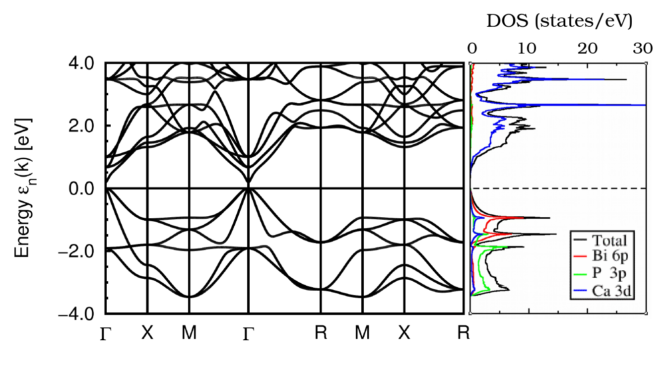
For general orientation, the electronic structure and DOS of a representative compound, Ca3BiP containing the largest and the next to smallest pnictide ions, is shown in Fig. 1b. A generic feature in this class of perovskites is that the smaller bands lie lower than the bands, making the larger ion (which conveniently also has the largest SOC) the one of interest in determining the band gap (or not) and subsequently the topological character. Since both A and B sites have cubic symmetry, both band complexes have threefold degeneracy at the point when SOC is neglected, and SOC separates the eigenvalues into and states, with the latter for forming the top of the valence bands.
In the conduction bands three sets of five bands dominate. Unexpectedly, a “free electron like” band that has no single dominant orbital character, discussed below, lies near the bottom of the conduction bands at and often is the band at the conduction band minimum (CBM). Since the site has tetragonal symmetry, the shell is split by the crystal field into a doublet and three singlets , relative to the local () axis. For some purposes it would be important to consider how these thirty orbitals on six ions form molecular orbitals on the octahedron. Actually performing and applying such a transformation is complicated by the fact that each ions’ orbitals are shared with two octahedra.
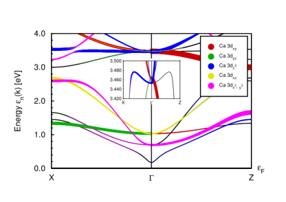
One fundamental interaction at and near is that of the states with the orbitals of the twelve ions coordinating it, and with the diffuse “” band. To assist understanding of the ordering of the characters at the point, the orbital characters in the band region of the apical Ca ion (whose local axis is along the direction) are plotted in Fig. 2. Ca and have orbital density oriented towards four nearest Bi-3 ions and two nearest P-3 ions respectively, and their orbital energies are close and are higher than for the other orbitals. The orbital lies lowest in energy, corresponding to an orbital density directed between negative ions, being lower than the highest orbital by 2.8 eV. This separation changes to 3.6 eV and 3.3 eV by replacing Ca with Sr and Ba respectively. The degenerate , orbitals lie about 0.4 eV above the orbital. The bands approach and mix with the bands around the point, with a substantial band gap throughout the rest of the zone.
Trends in band gaps. We here review the behavior of the gaps of the more stable members, which lie in the lower left triangle of Table I. We consider the bands without SOC, which are simpler from which to derive chemical trends. For NB (N on the B site), the Ca compounds have gaps that decrease from 0.85 eV to 0.48 eV for the progression from PA to BiA. The corresponding Sr compounds have smaller gaps, 0.45 eV to 0.25 eV, and for the Ba compounds there is band overlap (negative overlap). Moving to PB and on to BiB, there is no monotonic progression of gaps, but a clear trend to smaller or zero gaps at the B site atom becomes heavier. Evidently SOC, which splits the valence band maximum (VBM), will decrease the gap size and in some cases lead to gap inversion (reported in the table as zero gap or negative indirect gap).
Topological character. One of the motivations of this survey of 75 compounds was to begin to assess the likelihood of finding topological insulating, or also topological semimetal, phases in these antiperovskites. We return to this topic in Sec. IV. However, in Table I we have provided the topological index for the compounds and structures we have studied, for the GGA+SOC bands. In the lower left subdiagonal of Table I that contains the more stable ordering of the pairs, we find no topological bands in the NB column. However, moving to the heavier columns, many results are obtained. The profusion of these values appear at first sight to promote optimism. There are important caveats, however. First, GGA calculations are known to underestimate bandgaps in insulators. Self-energy corrections to the gap are discussed in Sec. III.3. Secondly, stability of these model compounds is an issue. Only a few have been reported, which we discuss in Sec. III.4. Some may be thermodynamically unstable with respect to more stable phases, while other may be dynamically unstable and distort to a lower symmetry structure with an altered electronic structure. We return to the question of topological character in Sec. IV.
III.3 Energy Gap Correction
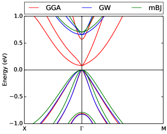
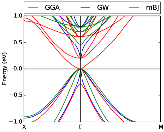
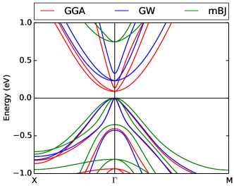
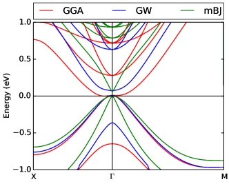
We define the inversion energy as the energy of the diffuse “s” band minus the energy of the VBM (which is that of the A site -band and has negative parity). (In the case the B site atom is N, the VBM is a strong admixture of and N character.) A negative inversion energy indicates the band inversion that is essential for topological character. Table 2 provides the inversion energy and band gap for GGA+SOC eigenvalues, with and without mBJ. Note that the band gap, once SOC is included, usually appears away from the point, thus is not equal to the inversion energy. The effect of including mBJ is a separation of conduction bands from valence bands (inversion energy) of 1.0, 0.7, 0.7, 0.6 eV for N, P, As, Sb, respectively, a very systematic trend independent of the cation Ca, Sr, Ba. The final (GGA+mBJ+SOC) band gap, if nonzero, is less regular because it occurs away from the point and is more dependent of details of the dispersion and inversion energy.
Only the BiSb compounds show negative inversion energy when the mBJ correction is included. has very small positive inversion energy (0.06 eV). The rest are normal insulators. Many of these inversion energies, positive or negative, are small enough that they can be manipulated by pressure or strain, with an example discussed in Sec. IV.
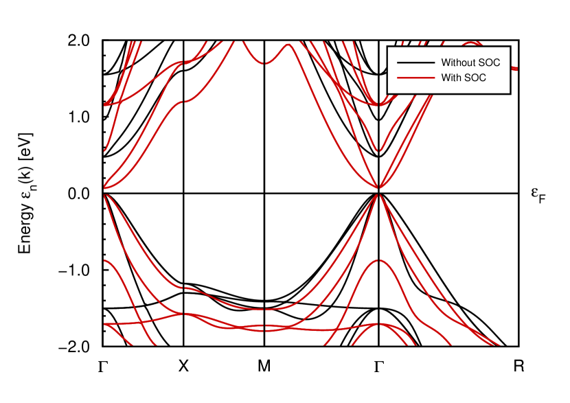
The bands of the four compounds we have chosen are shown in Fig. 3, all being based on Bi on the A site to provide the largest effect of SOC. Ca3BiN in Fig. 3a provides the reference normal insulator situation, with a two-fold level (A atom ) at the VBM and a doublet and a somewhat higher singlet in the lower conduction bands. The bands for the three cases, GGA(SOC), GGA(SOC)+mBJ, GGA(SOC)+GW∘, are aligned at the VBM. The corrections to the valence bands are not very important for our current considerations, but the two corrections are rather small but not necessarily similar. The conduction band corrections are larger in the region pictured, about 0.5 eV, and similar in the low energy region that is shown. Comparison between mBJ and GW corrections have been commented on previously.Camargo-Martinez2012
Fig. 3c shows the Sr analog, Sr3BiN. Its gap is smaller, but more interesting is that the conduction band singlet has dropped close to the doublet. Unexpectedly, the GW∘ correction has dropped to 0.15 eV while mBJ remains near 0.5 eV. The corrections in the valence bands remain small, and again the two corrections are not always similar.
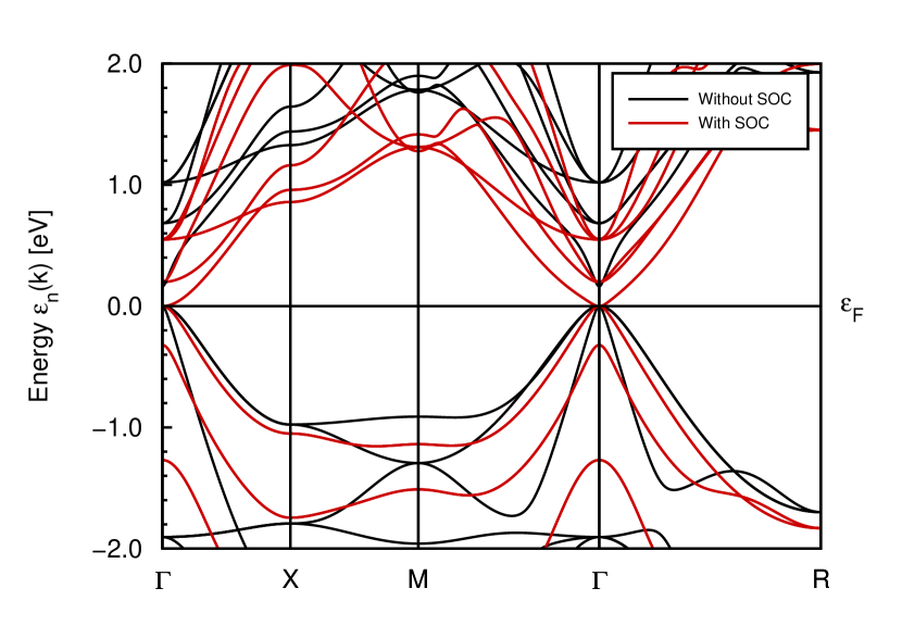
Band inversion occurs for Ca3BiP shown in Fig. 3b, due to the conduction band singlet dropping not only below the doublet, but also below the VBM doublet. One crucial result is that the band structure becomes that of a zero-gap semiconductor. Away from the bands hybridize, complicating the process of following the underlying bands. However, the inversion becomes clear when it is noticed that both self-energy corrections raise the GGA(SOC) eigenvalue at -0.3 eV, consistent with conduction eigenvalue character, which is also confirmed by its positive parity eigenvalue.
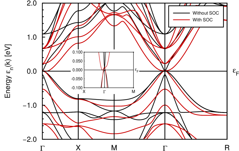
This behavior is repeated for Sr3BiAs shown in Fig. 3d, where the band orderings and corrections are somewhat different than in Ca3BiP and may be easier to follow. Even in GGA(SOC) the low energy band structure can be quite delicate, but becomes more so in the presence of self-energy corrections. This complex behavior will be explored on more detail elsewhere.
| Pn | N | P | As | Sb | |||||||||
| Ae | SOC | SOC + mBJ | mBJ effect | SOC | SOC + mBJ | mBJ effect | SOC | SOC + mBJ | mBJ effect | SOC | SOC + mBJ | mBJ effect | |
| Ca | Inversion Energy | 0.572 | 1.587 | 1.015 | -0.283 | 0.460 | 0.743 | -0.533 | 0.188 | 0.721 | -0.754 | -0.149 | 0.604 |
| Band Gap | 0.081 | 0.706 | 0.625 | 0 | 0.460 | 0.460 | 0 | 0.188 | 0.188 | 0 | 0 | 0 | |
| Sr | Inversion Energy | 0.133 | 1.138 | 1.005 | -0.458 | 0.286 | 0.744 | -0.658 | 0.063 | 0.721 | -0.831 | -0.226 | 0.605 |
| Band Gap | 0.088 | 0.746 | 0.658 | 0 | 0.286 | 0.286 | 0 | 0.063 | 0.063 | 0 | 0 | 0 | |
| Ba | Inversion Energy | 0.003 | 1.010 | 1.007 | -0.264 | 0.464 | 0.727 | -0.427 | 0.283 | 0.709 | -0.633 | -0.034 | 0.599 |
| Band Gap | 0 | 0.483 | 0.483 | 0 | 0.464 | 0.464 | 0 | 0.283 | 0.283 | 0 | 0 | 0 | |
III.4 Reported antiperovskites
Relatively few of this class of antiperovskite compounds have been synthesized, often without full characterization, and only nitrides. Most of these are based on the Ca2+ cation. All four of CaN were reported to be either semiconducting (=Bi,Sb) or insulating (=As,P).chern1992a Our calculated band gaps from Table 1 also indicate semiconducting states, as did previous work on some of these membersbilal2015b and the Sr and Ba counterparts (Sr,Ba)3(Sb,Bi)N.gaebler2004 When Bi is substituted by the smaller pnictides Sb, As, and P, the band gap increases, because as the electronegativity decreases, the energy level of the anion relative to the cation level decreases as well.
Structurally, the =Bi and Sb members of Ca3Bi are cubic, while (presumably) the size mismatch for the smaller ions =As and P anions led to orthorhombic distortion.chern1992b Niewa’s review reported Sr3(Sb,Bi)N as cubic, as well as Mg3(As,Sb)Nchi2002 which are not included in our study.niewa2013 In contrast, a hexagonal structure was reported for Ba3(Sb,Bi)N, built on face-sharing rather than corner-linked octahedra. Such a hexagonal structure tends to be favored by compounds containing alkaline-earth metal species with large radii. Coulomb repulsion between N in face-sharing octahedra and the resulting distance d(N-N) has been suggested to play a role in stabilizing the structure.niewa2013 ; gaebler2004 d(N-N) for Ba3(Sb,Bi)N is 3.30Å, which is sufficiently large to stabilize the hexagonal structure.
Some of these small gap compounds have been calculated to be promising thermoelectric materialsbilal2015 ; bilal2015b with high thermodynamic figure of merit. viz. Sr3(Sb,Bi)N.bilal2015 Magnetic susceptibility and electrical resistivity data indicate that the compounds are diamagnetic semiconductors. The optical band gaps of Sr3SbN and Sr3BiN are reported to be 1.15 eV and 0.89 eV, respectively.gaebler2004
First-principle calculations have been reported for some of the mentioned compounds, largely to assess specific properties such as their elastic behavior and optical response.haddadi2010 ; Rached2009 ; Jha2010 ; Ullah2016 ; Bidai2016 ; hichour2009b ; bilal2014 ; haddadi2009c ; hichour2010 ; moakafi2009 ; haddadi2009 Our survey should be useful in interpretation of those results, by connecting their computed properties to similarities and differences in their electronic structures.
IV On the Possibility of Topological Character
The invariant determines the topological nature of an insulator, and for inversion symmetric crystals the parity criteria proposed by Fu and KaneFu2007 determines the topological character. Specifically, the sum of the parities at occupied states at the time-reversal invariant momenta (TRIM) determines the primary invariant :
| (1) |
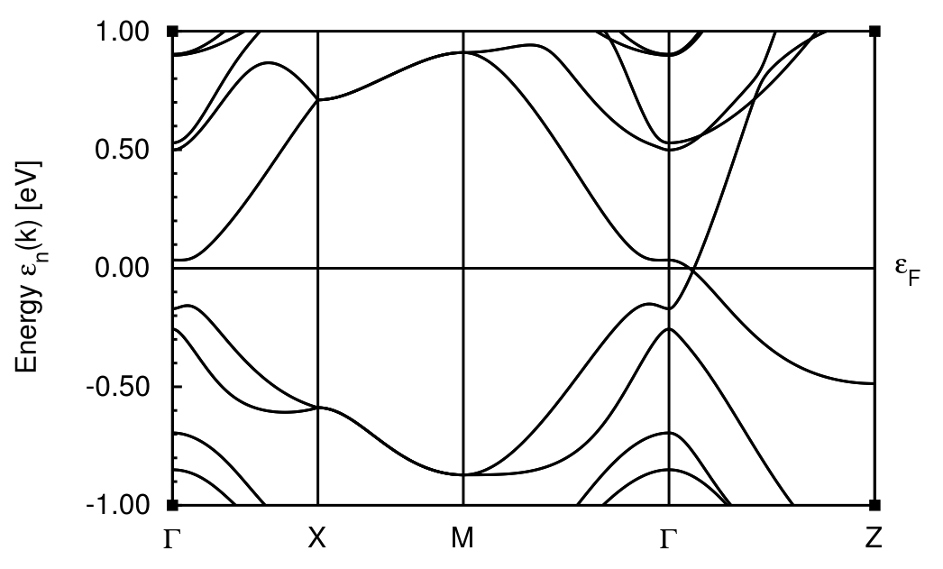
By studying Table 1 it can be found that the electronic structure and topological nature of these compounds can be classified into three categories: (i) small gap with a topologically trivial phase, viz. in Fig. 4a, (ii) the VBM and CBM touch at point with indices of (1;000), as for in Fig. 4b, and (iii) there are (usually tiny) electron and hole pockets along high symmetry lines with indices of (1;000) as in the example of in Fig. 4c.
For the first type, band inversion is not present for the cubic structure but the application of strain may lead to inversion and a topological material.Sun2010 For the second and third types (highlighted in bold in Table 1), the band inversion is induced by SOC of the heavy elements.Jin2013 No gap is opened, however, leaving these systems as topological semimetals. Strain can be used to induce a transition from topological semimetal to topological insulator, provided that the band overlapping (especially for type (iii)) is not greater than the effect of SOC.
A case study of will be used to demonstrate the role that interplay of SOC and strain play in band inversion of the second and third class above. Fig. 5 shows the schematic energy level diagram of at the point, along with the bands around for the same conditions. Cubic has an energy gap of 0.2 eV. At the point, the valence bands comprised of Bi characters and P characters have negative parities, while the character of the CBM has positive parity. (There are substantial gaps at all other TRIMs, so their contributions to Z2 are invariant to all changes and are the same for all of these antiperovskite compounds.) The strong SOC of Bi inverts the conduction band and the valence Bi bands. No gap is opened, however, resulting in a topological semimetal phase.
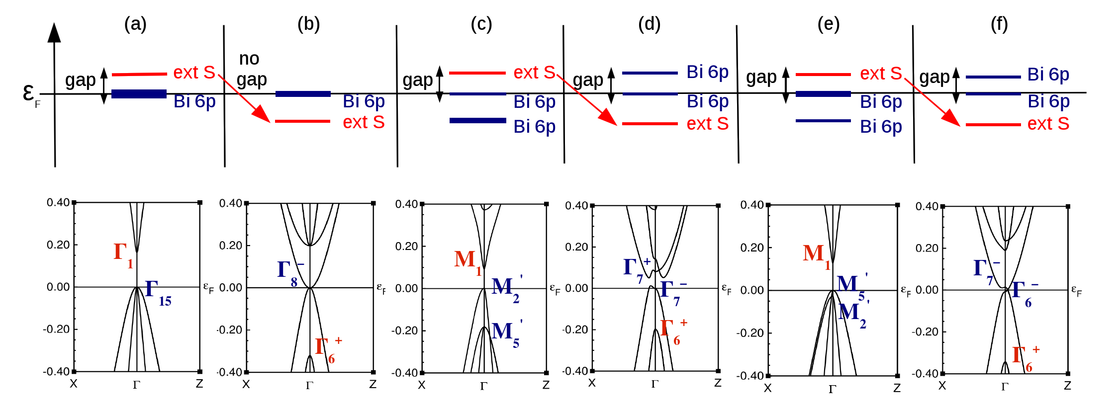
With a tetragonal compression of 5 along (001), the degeneracy is lifted and a small gap of 34 meV is produced while maintaining the inverted band ordering. The strain does not violate inversion symmetry, but merely splits the degeneracy of the band at the Fermi level into two sets of Kramer doublets, with odd parity below the Fermi level and even parity above, so the parity eigenvalues are unchanged. This mechanism is similar to that of and HgTe topological insulators.Fu2007 ; Ando2013 Although HgTe does not have inversion symmetry, it can be argued that this compound in group II-VI can be treated as adding a inversion symmetry breaking perturbation into group IV element, like Tin in the or gray phase.
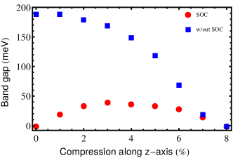
The transition from the topological semimetal state to a topological insulator can also be realized by compressing the lattice parameter by a few percent, which can be accomplished by growth of thin films on a substrate with the corresponding lattice parameter. As shown in Fig. 6, a small energy band gap with SOC is produced within this range, with a maximum gap of 40 meV occurring at compression. The band parity remain odd within this range, but goes back to even at 8 compression. On the other hand, uniaxial expansion along the c-axis opens up a gap except along , where a Dirac-like band crossing occurs, producing a topological Dirac semimetal (Fig. 5f). However, not all direction of strain application will open up a gap. For example, applying uniaxial strain along (111) direction does not open up a gap, because the Bi , and characters still remain equivalent.
V Structural (In)stability
The oxide perovskite structure is notoriously subject to distortion from the ideal cubic structure, for two primary reasons. First, perovskite is not a close-packed structure. Especially the BO2 (001) layer (viz. the CuO2 layer in high temperature superconducting cuprates) is not: atoms are aligned in rows with an empty site of square symmetry. Second, there is tension between the preferred lattice constants of the BO2 layer and the AO layer. The mismatch is quantified by Goldschmidt’s ratio, using established ionic radii and quantifying the mismatch as a percentage. It may be expected that these antiperovskites being studied may be subject to similar issues. Unfortunately, these antiperovskites comprise a new class of compounds for which appropriate ionic radii have not been established.
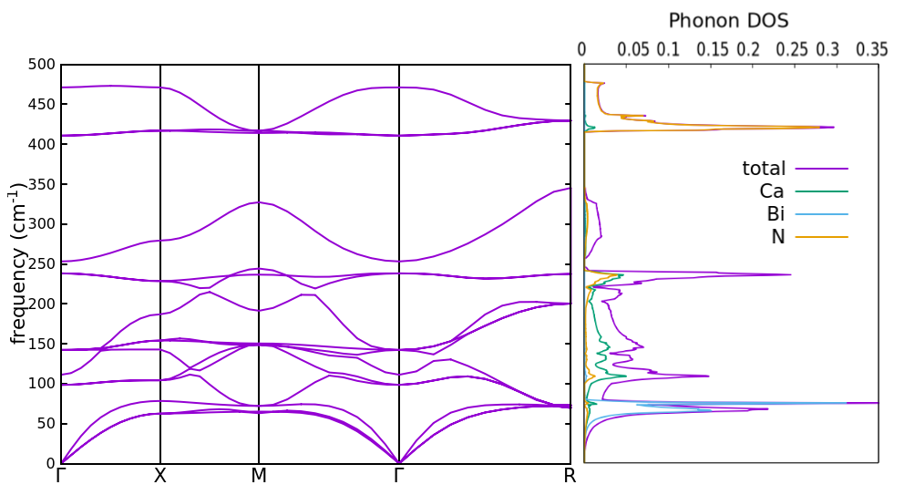
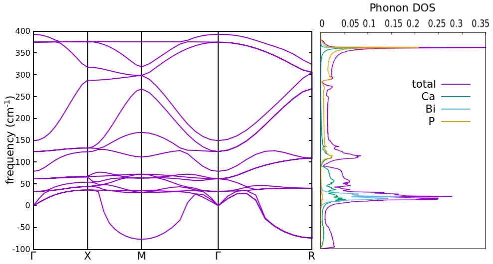
Calculation of the phonon spectrum is commonly used to assess dynamical stability of a compound. Antiperovskites with N atom at the B-site have been studied both experimentally and computationally bilal2015 ; bilal2015b ; chern1992b ; niewa2013 ; gaebler2004 ; haddadi2010 ; Rached2009 ; Jha2010 ; Ullah2016 ; Bidai2016 ; hichour2009b ; bilal2014 ; haddadi2009c ; hichour2010 ; moakafi2009 ; haddadi2009 . However, B-site cations other than N have not yet been incorporated into this structure. We have calculated the phonon dispersion curves for and for to assess their stability. The results are presented in Fig. 7.
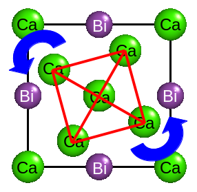
For , all frequencies are positive and the Bi atom dominates the acoustic frequencies up to 75 cm-1. Ca atoms dominate frequencies in the cm-1 range, while the light N atom oscillates in the highest frequency cm-1 region. The phonon spectrum of Ca3BiP is quite different. The overriding feature is the imaginary frequencies around both the M and R points of the zone. The atomic displacements at these points give insight into the structural instability; the unstable modes have Bi+Ca character. At the M point, the Bi and P atoms are fixed while the Ca atoms rotate around the principal axis, thus the crystal is unstable to such rotations. Allowing the octahedron to rotate around z-axis as shown in Fig. 8, the energy is lowered by 0.2 eV. The electronic rearrangement due to this distortion leaves as a conventional insulator.
Distortion of antiperovskites compounds with heavier elements, viz. BiSb with =Ca, Sr, and Ba, were studied as well. Distortions from cubic structure were favored by eV per formula unit. The resulting band structures are those of a Dirac semimetal, hosting Dirac points along the direction as shown for Ca3BiSb in Fig. 9. However, applying the mBJ correction widens that gap to around 0.4 eV and leaves them in conventional insulator states.
VI Summary
The stability, electronic structure and topological aspect of the class of isovalent antiperovskite alkaline earth-pnictide compounds have been studied using DFT. This class with pnictide other than N inside the octahedron is distorted with the octahedron rotated along a principal axis. The electronic structures of these compounds with SOC can be classified into three categories. First, one common class of the topological aspect is that the electronic structure is gapped with a topologically trivial phase. Second, a zero gap semiconductor with VBM and CBM touching at point with a invariant of 1;000. Third, a semimetal consists of electron or hole pockets of maximum 0.1 eV energy and band degenerate at point with a index of 1;000. Strain is required to produce a topological insulator. While the first type (e.g. Sun2010 ) needs both SOC and proper strain to have band ordering inverted, the second and third types (e.g. and ) only need SOC to induce the band inversion, giving a invariant of 1;000, but in a topological semimetal state, whereupon compressive strain may produce a transition to topological insulator. On the other hand, expansive strain may give rise to Dirac semimetals. With proper strain engineering, some may become a promising topological insulator and Dirac semimetal, as witness in and antiperovskite compounds.
VII Acknowledgments
We acknowledge useful comments from Theo Siegrist and Mas Subramanian about pnictide-based antiperovskite and nitride perovskite synthesis. This work was supported by the NSF DMREF program through grant DMR-1534719. Computational data for the compounds in Table I was uploaded to the DOE-supported Materials Project.
References
- [1] R. Sarmiento-Pérez, T. F. T. Cerqueira, S. Körbel, S. Botti and M. A. L. Marques, Prediction of Stable Nitride Perovskites, Chem. Mater. 27, 5957 (2015).
- [2] Y. Sun, X. Q. Chen, S. Yunoki, D. Li and Y. Li, New family of three-dimensional topological insulators with antiperovskite structure, Phys. Rev. Lett. , 216406 (2010).
- [3] M. Y. Chern, D. A. Vennos and F. J. DiSalvo, Synthesis, Structure, and Properties of Anti-perovskite Nitrides Ca3MN, M= P, As, Sb, Bi, Ge, Sn, and Pb, J. Solid State Chem. 96, 415 (1992).
- [4] M. Y. Chern, F. J. DiSalvo, J. Parise and J. A. Goldstone, The Structural Distortion of the Anti-perovskite Nitride Ca3AsN, J. Solid State Chem. 96, 426 (1992).
- [5] R. Niewa, Alkaline-earth Metal Nitrides of the Main-Group Elements: Crystal Structures and Properties of Inverse Perovskites, Z. f. anorg. allg. Chemie 639, 1699 (2013).
- [6] D. A. Papaconstantopoulos and W. E. Pickett, Ternary nitrides BiNCa3 and PbNCa3: Unusual ionic bonding in the antiperovskite structure, Phys. Rev. B 45, 4008 (1992).
- [7] J. P. Perdew, K. Burke and M. Ernzerhof, Generalized gradient approximation made simple, Phys. Rev. Lett. , 3865 (1996).
- [8] K. Koepernik and H. Eschrig, Full-potential nonorthogonal local-orbital minimum-basis band-structure scheme, Phys. Rev. B , 1743 (1999).
- [9] A. D. Becke and E. R. Johnson, A simple effective potential for exchange, J. Chem. Phys. , 221101 (2006).
- [10] F. Tran, P. Blaha and K. Schwarz, Band gap calculations with Becke-Johnson exchange potential, J. Phys.: Condens. Matter. , 196208 (2007).
- [11] F. Tran and P. Blaha, Accurate Band Gaps of Semiconductors and Insulators with a Semilocal Exchange-Correlation Potential, Phys. Rev. Lett. , 226401 (2009).
- [12] H. Jiang, R. I. Gomez-abal, X. Li, C. Meisenbichler, C. Ambrosch-Draxl and M. Scheffler, FHI-gap: a code based on the all-electron augmented plane wave method, Comp. Phys. Commun. 184, 348 (2013).
- [13] H. Jiang and P. Blaha, GW with linearized augmented plane waves extended by high-energy local orbitals, Phys. Rev. B , 115203 (2016).
- [14] P. Blaha, K. Schwarz, G. Madsen, D. Kvasnicka and J. Luitz, WIEN2k: An Augmented Plane Wave + Local Orbitals Program for Calculating Crystal Properties, (Karlheinz Schwarz, Techn. Universität Wien, Austria), 2001.
- [15] J. A. Camargo-Mart nez and R. Baquero, Performance of the modified Becke-Johnson potential for semiconductors, Phys. Rev. B , 195106 (2012).
- [16] M. Bilal, S. Jalali-Asadabadi, R. Ahmad, and I. Ahmad, Electronic Properties of Antiperovskite Materials from State-of-the-Art Density Functional Theory, J. Chem. , 495131 (2015).
- [17] F. Gäbler, M. Kirchner, W. Schnelle, U. Schwarz, M. Schmitt, H. Rosner and R. Niewa, (Sr3N)E and (Ba3N)E (E = Sb, Bi): Synthesis, Crystal Structures, and Physical Properties, Z. anorg. allg. Chem. 630, 2292 (2004).
- [18] E. O. Chi, W. S. Kim, N. H. Hur and D. Jung, New Mg-based antiperovskites PnNMg3 (Pn=As, Sb), J. Solid State Commun. 121, 309 (2002).
- [19] M. Bilal, Saifullah, M. Shafiq, B. Khan, H. A. R. Aliabad, S. J. Asadabadid, R. Ahmad and I. Ahmad, Antiperovskite compounds SbNSr3 and BiNSr3: Potential candidates for thermoelectric renewable energy generators, Phys. Lett. A 379, 2067 (2015).
- [20] K. Haddadi, A. Bouhemadou and L. Louail, Structural, elastic and electronic properties of the hexagonal anti-perovskites SbNBa3 and BiNBa3, Comput. Mater. Sci. 48, 711 (2010).
- [21] M. Hichour, D. Rached, M. Rabah, S. Benalia, R. Khenata and F. Semari, Structural and elastic properties of antiperovskites XNBa3 (X=As, Sb) under pressure effect, Physica B: Condens. Matt. 404, 4034 (2009).
- [22] D. Rached, M. Hichour, M. Rabah, S. Benalia, H. Rached and R. Khenata, Prediction study of the structural, elastic, electronic and optical properties of the antiperovskite BiNBa3, Solid State Commun. , 2002 (2009).
- [23] P. K. Jha and S. K. Gupta, First principles lattice dynamical study of the cubic antiperovskite compounds AsNBa3 and SbNBa3, Solid State Commun. , 1650 (2010).
- [24] I. Ullah, G. Murtaza, R. Khenata, A. Mahmood, M. Muzzamil, N. Amin and M. Saleh, Structural and Optoelectronic Properties of X3ZN (X = Ca, Sr, Ba; Z = As, Sb, Bi) Anti-Perovskite Compounds, J. Elec. Mater. , 3059 (2016).
- [25] K. Bidai, M. Ameri and I. Ameri, A first-principles study on structural, thermodynamics and elastic properties of XNBa3 (X=As, Sb) under pressure and temperature effect, Optik-Int. J. Light Electron Opt. , 3250 (2016).
- [26] M. Bilal, I. Ahmad, H. A. R. Aliabad and S. J. Asadabadi, Detailed DFT studies of the band profiles and optical properties of antiperovskites SbNCa3 and BiNCa3, Comput. Mater. Sci. 85, 310 (2014).
- [27] K. Haddadi, A. Bouhemadou, L. Louail, F. Rahal and S. Maabed, Prediction study of the structural, elastic and electronic properties of ANSr3 (A=As, Sb and Bi), Comput. Mater. Sci. 46, 881 (2009).
- [28] M. Hichour, R. Khenata, D. Rached, M. Hachemaoui, A. Bouhemadou, A. H. Reshak and F. Semari, FP-APW+lo study of the elastic, electronic and optical properties for the cubic antiperovskite ANSr3 (A=As, Sb and Bi) under pressure effect, Physica B: Condens. Matt. 405, 1894 (2010).
- [29] M. Moakafi, R. Khenata, A. Bouhemadou, F. Semari, A. H. Reshak and M. Rabah, Elastic, electronic and optical properties of cubic antiperovskites SbNCa3 and BiNCa3, Comput. Mater. Sci. 46, 1051 (2009).
- [30] K. Haddadi, A. Bouhemadou, L. Louail, S. Maabed and D. Maouche, Structural and elastic properties under pressure effect of the cubic antiperovskite compounds ANCa3 (A=P, As, Sb, and Bi), Phys. Lett. A 373, 1777 (2009).
- [31] L. Fu and C. L. Kane, Topological insulators with inversion symmetry, Phys. Rev. B , 045302 (2007).
- [32] H. Jin, S. H. Rhim, J. Im and A. J. Freeman, Topological oxide insulator in cubic perovskite structure, Sci. Rep. , 1651 (2013).
- [33] Y. Ando, Topological insulator materials, J. Phys. Soc. Jpn. , 102001 (2013).