Atomic-scale identification of novel planar defect phases in heteroepitaxial YBa2Cu3O7-δ thin films
Abstract
We have discovered two novel types of planar defects that appear in heteroepitaxial YBa2Cu3O7-δ (YBCO123) thin films, grown by pulsed-laser deposition (PLD) either with or without a La2/3Ca1/3MnO3 (LCMO) overlayer, using the combination of high-angle annular dark-field scanning transmission electron microscopy (HAADF-STEM) imaging and electron energy loss spectroscopy (EELS) mapping for unambiguous identification. These planar lattice defects are based on the intergrowth of either a BaO plane between two CuO chains or multiple Y-O layers between two CuO2 planes, resulting in non-stoichiometric layer sequences that could directly impact the high- superconductivity.
Recently, a great deal of interest has been focused on thin-film heterostructures comprising YBa2Cu3O7-δ (YBCO123) and other complex oxides, because of novel interfacial interactionsZhang et al. (2009); Varela et al. (2003); Habermeier et al. (2001) that could affect the high-critical temperature () superconductivity.Bacca et al. (2004); Chakhalian et al. (2007)YBCO123 in heteroepitaxial form is known to contain a variety of crystalline defects, as its layered perovskite structure is sensitive to lattice strains induced by the epitaxial mismatch.Ramesh et al. (1992); Zhang et al. (2013); Fendorf et al. (1990); Foltyn et al. (2007); Grigis, Schamm, and Dorignac (1999); Domengès et al. (1991) Since such defects may also affect the microscopic pairing mechanism, it is important to determine their lattice structures at the atomic scale. There is solid experimental evidence to suggest that the interfacial lattice mismatch in heteroepitaxial thin films of complex oxides can, through induced lattice strains, affect the microstructure in the film.
In an earlier study of YBCO123 thin films heterostructured with La2/3Ca1/3MnO3 (LCMO) overlayers, we observed nanoscale domains of YBCO124 and YBCO247 containing CuO-chain intergrowths, which were attributed to the heteroepitaxial strain and also shown to cause attenuation of .Zhang et al. (2013) In the present study, we focus on defect phases associated with Ba-O and Y-O intergrowths in heteroepitaxial YBCO123 thin films both with and without LCMO overlayers. Two novel types of planar defects are unequivocally observed, both deviating from the normal stacking sequence (CuO-BaO-CuO2-Y-CuO2-BaO) of the YBCO123 lattice. The first defect type (henceforth called type D1) consists of a BaO layer sandwiched between two CuO-chain layers. The second defect type consists of the addition of either one (type D2) or two (type D2’) extra Y-O layers between the CuO2 planes.
The samples used in this study include single-layer YBCO123 and bi-layer LCMO/YBCO123 thin films. The layer thickness of YBCO123 was either 25 nm or 50 nm, while the LCMO overlayer thickness was 25 nm. The films were epitaxially grown on (001)-oriented (La,Sr)(Al,Ta)O3 (LSAT) substrates using pulsed laser-ablated deposition (PLD). The films were annealed in-situ by slowly cooling from to in 1 atm of O2 at a rate of /min. Cross-section of the resulting samples were then prepared by FIB and thinned with an Ar beam to 40 - 45 nm in a Fischione Nanomill 1040 instrument operated at 900eV. Imaging by scanning transmission electron microscopy (STEM) and spectroscopy of electron energy loss (EELS) were carried out with an FEI Titan3 TEM, equipped with a CEOS-designed hexapole-based aberration corrector for both the probe-forming lens and imaging lens. The instrument is fitted with a high brightness electron source, in order to achieve sub-angstrom resolution Botton, Lazar, and Dwyer (2010). Measurements were performed at 200 keV in order to reduce knock-on damage. EELS spectra were recorded on a high resolution Gatan GIF Tridiem spectrometer. The convergence semi-angle for STEM was 20 mrad, the inner acceptance semi-angle for High Angle Annular Dark Field (HAADF) imaging was 50 mrad, the collection semi-angle for EELS was 110 mrad.
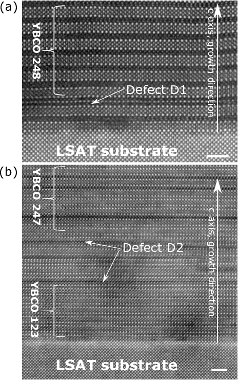
Fig. 1 shows -contrast STEM images (in which the intensity is proportional to , and is the atomic number) taken using the HAADF technique on single-layer YBCO123 films. As was seen in our previous study, local domains of YBCO248 and YBCO247, resulting from intergrowth of CuO chains, are present in the matrix of YBCO123. In the case of orthorhombic YBCO123 grown on and between cubic perovskites, Cu-O stacking faults have previously been observed Fendorf et al. (1990) and are associated with the formation of defect phases such as YBCO124, YBCO247, YBCO125 and YBCO249 (for which the first number corresponds to the number of Y in a unit cell and the subsequent second and third number Ba and Cu, respectively), depending on the number of CuO chains per unit cell.Ramesh et al. (1992); Grigis, Schamm, and Dorignac (1999) Also visible in Fig. 1(a) are type D1 defects, which is related to an excess BaO layer between two CuOx chains. In previous studies Ramesh et al. (1992); Grigis, Schamm, and Dorignac (1999), these defects were interpreted mainly as YO-CuO or as BaO/YO interconversion from HRTEM image analysis; however, Domenges et al.Domengès et al. (1991) has pointed out the unfavourable nature of the YO-CuO structure, which would distort the environment of the YO8 cage. More recently, Gazquez et al.Gazquez et al. (2012) have interpreted this defect type in terms of Ba-CuOx intergrowth. In our present study, atomic-scale HAADF imaging was used in conjunction with elemental EELS mapping to elucidate the exact lattice structure and atomic composition of the D1 defect structure, as we present below.
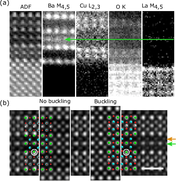
As shown in 2(a), the D1 defect type we observed can be systematically identified in terms of BaO-CuO1-δ intergrowth using atomic-scale EELS mapping whereby an extra Ba layer is detected in the Ba M4,5 map (pointed out with a green arrow in 2(a)). The D2 defect type, according to the elemental maps seen on Figure 3(a) (deduced from the Y L2,3 edge intensity), contain additional Y-O2 layers between the CuO2 planes (shown by red and blue arrows in 3(b)). Care was taken such that the application of weighted principal component analysis (PCA) within the multivariate statistical analysis plugin developed by M. Watanabe Bosman et al. (2006) was only increasing the already good contrast in the elemental maps and not altering it or introducing artefacts. In Fig. 2(b) we first note that the Ba atoms in the BaO layer are displaced away from the CuO chainHott et al. (2004); Tsuei and Kirtley (2000). This displacement is similar to the buckling distortion seen in the CuO2 plane of all cuprate superconductors, where the four oxygen atoms from the CuO2 plane are displaced towards the Y spacer layer to form a CuO5 pyramid with the apical oxygen atoms. Although buckling of the CuO2 planes is expected to have a stronger effect on the of YBCO123Sardar and Bhattacharjee (2001); Chmaissem et al. (1999) than buckling of the BaO planes, the latter does significantly increase the Ba-Ba separation about the CuO-chain layer.Okamura et al. (1987); Tsuei and Kirtley (2000) This increased Ba-Ba separation (easily noticeable from HAADF-STEM images) effectively increases the Cu-O apical bond length, and could thus inhibit the charge transfer between chain and plane. Taking into account these buckling effects on the YBCO123 latticeAkimitsu (1992); Swinnea and Steinfink (1987); Sato et al. (1988),11footnotemark: 1, we consider two structural models for the D1 defect, which are overlaid as simulated images in Fig. 2(b) for side-by-side comparison with the experimental HAADF images. HAADF images were simulated using the multislice method carried out with the code developed by Kirkland.Kirkland et al. (1991) A Gaussian broadening was applied to these simulated images to consider, as a first approximation, the finite source size and to improve the accuracy of the comparison with the experimental data.Nellist and Rodenburg (1994) The experimental HAADF images were Fourier-filtered to reduce the noise. For the lattice position of Ba, better agreement with the experimental image is obtained by assuming a similar buckling in the outer BaO layers (highlighted by open circle) as in fully-oxygenated YBCO123 (YBa2Cu3O7), and an absence of distortion in the central BaO plane. The larger spacing between the BaO planes on each side of the defect (9.2 Å for empty chains versus 8.7 Å for full chains) indirectly suggests (in conjunction with the absence of heavy atoms from HAADF imaging) that the CuO chains are oxygen-deficient in this particular area (see Supplementary material). The simulated image with empty chains surrounding the BaO defect layer is shown as an overlay in Figure 2(b), and is in excellent agreement with the experimental image. The dimmer intensity of both the O K-edge EELS map shown in Fig. 2(a) and the HAADF images in Fig. 1(a) gives further indication that this intercalated BaO plane is surrounded by oxygen-deficient CuO1-δ chains. Therefore, we can infer the defect structure D1 as having a local stoichiometry of YBa3Cu4O9-δ. The difference between these values is several times greater than the precision achievable through STEM imaging (around 10pm) making these assumptions on oxygen stoichiometry trustworthy.
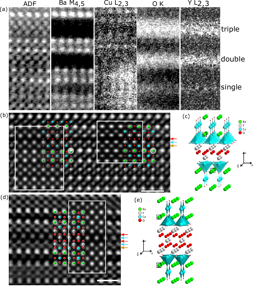
The D2 defect type we observed is shown in Fig. 3(a) and 3(b) and also visible in Fig. 1(b), and to our best knowledge has never been reported before in YBCO compounds. HAADF images of the ribbon structures formed by the double-layered (D2)(Y-O2-Y) and triple-layered (D2’) (Y-O2-Y-O2-Y) intergrowths are shown in Fig. 3(b) and 3(d) respectively. It is worth noting that a very dark band between the Y bright layers may indicate the presence of an additional layer (of a low- element) not visible by HAADF imaging. Precise structural determination of this defect type is non-trivial, requiring a priori knowledge about ideal interplanar distances for YBCO123Akimitsu (1992); Swinnea and Steinfink (1987); Sato et al. (1988) and structural comparisons with other cuprate superconductors, as discussed below.111 According to structural refinement by x-ray crystallography, the Ba atom is vertically displaced by 0.32 Å (0.499 Å) relative to the apical O for fully-oxygenated (under-oxygenated) YBCO123 Sato et al. (1988); Okamura et al. (1987). Thus the Ba-Ba distance about the CuO-chain layer is 4.336 Å or 4.598 Å respectively, which is sizable compared with the value of 3.7 Å for an ideal lattice with no bucklingAkimitsu (1992)..
In a general manner, high- cuprate superconductors can be represented by the formula unit AmE2Yn-1CunO2n+m+2+y where A and E denote atoms in the EO/(AOx)m/EO charge reservoir (here E=Ba and A=Cu, stacked with n CuO2 superconducting planes and n-1 Y spacer layers) and conveniently abbreviated as A-m2(n-1)n.Hott et al. (2004) By this nomenclature, YBCO123 can be represented as Cu-1212. The spacing between the oxygen atoms of the CuO2 plane and Y layers is 1.418 Å in YBa2Cu3O7Sato et al. (1988), due to the buckling of the CuO2 planes discussed earlier (O shifted towards the Y plane). Similarly in the Pr-based cuprate of the Hg-1222 and Tl-1222 families Domengès et al. (1991); Hervieu et al. (1995), a second Pr plane is intercalated between the CuO2 planes, the distance between the Pr and O ions being 1.4 Å. This spacing is remarkably identical to the spacing observed between each Pr layer and the central O2 layer in this 1222 structure.Domengès et al. (1991); Hervieu et al. (1995) In the HAADF image shown in Fig. 3(b), the spacing between the two Y layers is about twice as large (2.8 Å) as the spacing between the Y and CuO2 planes, suggesting the presence of a similar O2 plane between the Y layers in the D2 defect structure.
Using these structural analogies, we establish a model for the double-layered Y-O2 defect as shown in Fig. 3(c). A model for the triple-layered Y-O2 defect can be similarly established as shown in Fig. 3(e). Details of our structural models, corresponding to the D2 and D2’ defect types, are given respectively in Supplementary Materials. HAADF images were also simulated from the D2 and D2’ defect lattices plotted as overlays in Fig. 3(b) and 3(d) for comparison with the experimental HAADF images. We note that, as in the case of the BaO defect discussed above, the Ba-Ba spacing shows better agreement between the simulated and experimental images when buckling of the CuO2 and BaO planes is conserved as in the previous case. In terms of interplanar spacings, the Ba and Cu positions in the experimental image are better explained by assuming oxygen-rich CuO chains on both sides of this defective BaO-CuO2-Y-O2-Y-CuO2-BaO unit (see Supplementary material).
As for the D2 defect shown in Fig. 3(b), comparison of the Ba-Ba spacing between the experimental image and the simulated image for under-oxygenated YBCO123 (YBa2Cu3O6) suggests that these CuO1-δ chains are oxygen-deficient in this particular area. Thus the D2 and D2’ defects correspond to local stoichiometries of Y2Ba2Cu3O10 and Y3Ba2Cu3O12-δ respectively. Here it should be noted that O K-edge maps cannot be directly used to determine oxygen content, as the contrast is strongly influenced by channeling of the neighboring columns of heavy atoms; nonetheless a hint on the O content in layers with the same environment (or coordination sphere) can be postulated. In the oxygen mapping of Fig. 3(a), we do notice a strong increase in the intensity of the -edge map versus the number of Y layers, confirming the presence of oxygen atoms between the Y planes.
It is remarkable to note that, while neither D1, D2 and D2’ defect structure appears to modify the buckling of the BaO and CuO2 planes, the zigzag ribbon structure of the double Y-O2 layer in the D2 case effectively breaks inversion symmetry of the YBCO123 lattice about the Y plane. This structural peculiarity is physically significant, in that the resulting lack of a center of symmetry along the c-axis could profoundly affect the electron pairing in the CuO2 layersBauer and Sigrist (2012); Tsuei and Kirtley (2000), either by allowing spin-singlet/triplet mixing or by introducing a Rashba spin-orbit term in the pairing Hamiltonian, especially when strong electron correlations are present. Prior studies of such non-centrosymmetric superconductors have been limited to a few intermetallic materials with rather low , such as CePt3Si, Li2Pd3B and KOs2O6Bauer et al. (2004); Yuan et al. (2006); Shibauchi et al. (2006). Our observation of the D2 defect structure, and its role in forming a YBCO lattice with broken inversion symmetry, suggests that it is potentially useful as a building block for synthesizing non-centrosymmetric high- superconductors via heteroepitaxial oxide engineering. According to geometrical phase analysis (see supplementary material for details) the D2 type defect locally affects the and family of planes but not the planes. These D2 defects are linked to some antiphase boundary delimiting an intergrowth region. This boundary might act as pinning center for vortices as discussed previously for BaZrO3 or other type of foreign intergrowths.Gazquez et al. (2012); Llordés et al. (2012); Guzman et al. (2013) In contrast, the defect D1 does not influence any of the three aforementioned families of planes.
Finally, we discuss generic implications of the defect structures identified above, in relation to the superconducting properties of the high- cuprates. First, it should be noted that since the volume fraction of these defects is rather small, a direct measurement of their influence on the superconductivity of the film is thus not possible. Nevertheless, by virtue of their novel stacking sequence, the primary effects of these defect structures on fully-oxygenated YBCO123 (structure type 1212) can be inferred from analogies with similar defect structures observed in the bulk form of more complex cuprates. For the D1 defect (structure type 2312), carrier localization within this BaO-CuO1-δ-BaO-CuO1-δ-BaO block may occur as a result of inhibited conduction within the oxygen-depleted chains. For the D2 defect (structure type 1222), insertion of YO2 layers (which follows the fluorite structureGrigoraviciute, Yamauchi, and Karppinen (2007); Martin et al. (1989)) between the CuO2 planes increases the spacing between the two CuO2 planes, and could thus directly affect as in the case of Tl- and Hg-based cuprates.Domengès et al. (1989); Hervieu et al. (1995) Furthermore, for the D2 defect, it is conceivable for excess oxygen within the YO2 layers to more tightly bind together the CuO2 layers and reduce their spacing to the Y plane, thus enhancing the hole concentration within them.Abrikosov (1999); Bianconi, Poccia, and Ricci (2010) Since the high- cuprates that contain these fluorite-type defects are predominantly tetragonal, we can infer that the presence of these defects in YBCO123 tends to weaken its orthorhombicity, thereby reducing the oxygen content and thus the hole concentration in the CuO chains.
In summary, we have performed atomic-scale STEM, via Z-contrast HAADF imaging and elemental EELS mapping, of defect structures in heteroepitaxial YBCO123 thin-film samples grown on LSAT substrates by PLD. We focused on the observation of two novel types of planar defects associated with Ba-O and Y-O intergrowths, and used atomic-scale data analysis with model simulations to unequivocally identify their lattice structures. One defect type (D1) consists of a BaO layer between two oxygen-deficient CuO1-δ chains corresponding to the formula unit of YBa4Cu4O9-δ; the other defect type (D2 and D2’) consists of either a Y-O2-Y or Y-O2-Y-O2-Y fluorite-like block sandwiched between the CuO2 planes, corresponding to Y2Ba2Cu4O10 and YBa3Cu4O12-δ respectively. While the D1 defect is expected to localize charge carriers in the CuO chains, the D2 and D2’ defects are expected to directly impact the high- pairing by increasing the CuO2 bilayer spacing. Remarkably, the D2 defect is shown to break inversion symmetry of the YBCO123 lattice, and could thus serve as a building block for synthesizing non-centrosymmetric high- superconductors. Our STEM study demonstrates that the combined use of atomic-scale HAADF imaging and EELS mapping can effectively identify defect structures in complex materials.
Acknowledgements
We are thankful to Julia Huang for FIB TEM sample preparation. This work is supported by NSERC (through Discovery Grants to GAB and JYTW) and CIFAR. The electron microscopy work was carried out at the Canadian Centre for Electron Microscopy, a National Facility supported by McMaster University, the Canada Foundation for Innovation and NSERC. N.G. acknowledges H. Idrissi for useful discussions.
References
- Zhang et al. (2009) Z. L. Zhang, U. Kaiser, S. Soltan, H.-U. Habermeier, and B. Keimer, Applied Physics Letters 95, 242505 (2009).
- Varela et al. (2003) M. Varela, A. R. Lupini, S. J. Pennycook, Z. Sefrioui, and J. Santamaria, Solid-State Electronics 47, 2245 (2003).
- Habermeier et al. (2001) H.-U. Habermeier, G. Cristiani, R. Kremer, O. Lebedev, and G. van Tendeloo, Physica C: Superconductivity 364-365, 298 (2001).
- Bacca et al. (2004) E. Bacca, F. Pérez, K. Gross, P. Prieto, O. Morán, and R. Hott, Annalen der Physik 13, 93 (2004).
- Chakhalian et al. (2007) J. Chakhalian, J. W. Freeland, H.-U. Habermeier, G. Cristiani, G. Khaliullin, M. van Veenendaal, and B. Keimer, Science (New York, N.Y.) 318, 1114 (2007).
- Ramesh et al. (1992) R. Ramesh, A. Inam, T. Sands, and C. Rogers, Materials Science and Engineering: B 14, 188 (1992).
- Zhang et al. (2013) H. Zhang, N. Gauquelin, G. A. Botton, and J. Y. T. Wei, Applied Physics Letters 103, 052606 (2013).
- Fendorf et al. (1990) M. Fendorf, C. P. Burmester, L. T. Wille, and R. Gronsky, Applied Physics Letters 57, 2481 (1990).
- Foltyn et al. (2007) S. R. Foltyn, L. Civale, J. L. Macmanus-Driscoll, Q. X. Jia, B. Maiorov, H. Wang, and M. Maley, Nature materials 6, 631 (2007).
- Grigis, Schamm, and Dorignac (1999) C. Grigis, S. Schamm, and D. Dorignac, Journal of Materials Research 14, 2732 (1999).
- Domengès et al. (1991) B. Domengès, M. Hervieu, B. Raveau, J. Karpinski, E. Kaldis, and S. Rusiecki, Journal of Solid State Chemistry 93, 316 (1991).
- Botton, Lazar, and Dwyer (2010) G. A. Botton, S. Lazar, and C. Dwyer, Ultramicroscopy 110, 926 (2010).
- Gazquez et al. (2012) J. Gazquez, M. Coll, N. Roma, F. Sandiumenge, T. Puig, and X. Obradors, Superconductor Science and Technology 25, 065009 (2012).
- Bosman et al. (2006) M. Bosman, M. Watanabe, D. T. L. Alexander, and V. J. Keast, Ultramicroscopy 106, 1024 (2006).
- Hott et al. (2004) R. Hott, R. Kleiner, T. Wolf, and G. Zwicknagl, in Frontiers in Superconducting Materials, edited by Prof. Dr. Anant V. Narlikar (Springer Berlin Heidelberg, 2004) pp. 1–70.
- Tsuei and Kirtley (2000) C. C. Tsuei and J. R. Kirtley, Reviews of Modern Physics 72, 969 (2000).
- Sardar and Bhattacharjee (2001) M. Sardar and S. Bhattacharjee, Physica C: Superconductivity 349, 89 (2001).
- Chmaissem et al. (1999) O. Chmaissem, J. D. Jorgensen, S. Short, A. Knizhnik, Y. Eckstein, and H. Shaked, Nature 397, 45 (1999).
- Okamura et al. (1987) F. P. Okamura, S. Sueno, I. Nakai, and A. Ono, Proceedings of the Japan Academy. Ser. B: Physical and Biological Sciences 63, 165 (1987).
- Akimitsu (1992) J. Akimitsu, Japanese Journal of Applied Physics Series 7, 20 (1992).
- Swinnea and Steinfink (1987) J. S. Swinnea and H. Steinfink, Journal of Materials Research 2, 424 (1987).
- Sato et al. (1988) S. Sato, I. Nakada, T. Kohara, and Y. Oda, Acta Crystallographica Section C 44, 11 (1988).
- Note (1) According to structural refinement by x-ray crystallography, the Ba atom is vertically displaced by 0.32 Å (0.499 Å) relative to the apical O for fully-oxygenated (under-oxygenated) YBCO123 Sato et al. (1988); Okamura et al. (1987). Thus the Ba-Ba distance about the CuO-chain layer is 4.336 Å or 4.598 Å respectively, which is sizable compared with the value of 3.7 Å for an ideal lattice with no bucklingAkimitsu (1992).
- Kirkland et al. (1991) A. I. Kirkland, D. A. Jefferson, D. Tang, and P. P. Edwards, Proceedings of the Royal Society A: Mathematical, Physical and Engineering Sciences 434, 279 (1991).
- Nellist and Rodenburg (1994) P. Nellist and J. Rodenburg, Ultramicroscopy 54, 61 (1994).
- Hervieu et al. (1995) M. Hervieu, G. Van Tendeloo, C. Michel, C. Martin, A. Maignan, and B. Raveau, Journal of Solid State Chemistry 115, 525 (1995).
- Bauer and Sigrist (2012) E. Bauer and M. Sigrist, eds., Non-Centrosymmetric Superconductors: Introduction and Overview, lecture no ed., Vol. 847 (Springer-Verlag Berlin Heidelberg, 2012).
- Bauer et al. (2004) E. Bauer, G. Hilscher, H. Michor, C. Paul, E. W. Scheidt, A. Gribanov, Y. Seropegin, H. Noël, M. Sigrist, and P. Rogl, Physical Review Letters 92, 027003 (2004).
- Yuan et al. (2006) H. Q. Yuan, D. F. Agterberg, N. Hayashi, P. Badica, D. Vandervelde, K. Togano, M. Sigrist, and M. B. Salamon, Physical Review Letters 97 (2006).
- Shibauchi et al. (2006) T. Shibauchi, L. Krusin-Elbaum, Y. Kasahara, Y. Shimono, Y. Matsuda, R. D. McDonald, C. H. Mielke, S. Yonezawa, Z. Hiroi, M. Arai, T. Kita, G. Blatter, and M. Sigrist, Physical Review B 74 (2006).
- Llordés et al. (2012) A. Llordés, A. Palau, J. Gázquez, M. Coll, R. Vlad, A. Pomar, J. Arbiol, R. Guzmán, S. Ye, V. Rouco, F. Sandiumenge, S. Ricart, T. Puig, M. Varela, D. Chateigner, J. Vanacken, J. Gutiérrez, V. Moshchalkov, G. Deutscher, C. Magen, and X. Obradors, Nature materials 11, 329 (2012).
- Guzman et al. (2013) R. Guzman, J. Gazquez, V. Rouco, a. Palau, C. Magen, M. Varela, J. Arbiol, X. Obradors, and T. Puig, Applied Physics Letters 102, 081906 (2013).
- Grigoraviciute, Yamauchi, and Karppinen (2007) I. Grigoraviciute, H. Yamauchi, and M. Karppinen, Journal of the American Chemical Society 129, 2593 (2007).
- Martin et al. (1989) C. Martin, D. Bourgault, M. Hervieu, C. Michel, J. Provost, and B. Raveau, Modern Physics Letters B 03, 993 (1989).
- Domengès et al. (1989) B. Domengès, M. Hervieu, C. Martin, D. Bourgault, C. Michel, and B. Raveau, Phase Transitions 19, 231 (1989).
- Abrikosov (1999) A. A. Abrikosov, Physica C: Superconductivity 341-348, 97 (1999).
- Bianconi, Poccia, and Ricci (2010) A. Bianconi, N. Poccia, and A. Ricci, Advances in Condensed Matter Physics 2010 (2010).