Sensitive spin detection using an on-chip SQUID-waveguide resonator
Abstract
Precise detection of spin resonance is of paramount importance to achieve coherent spin control in quantum computing. We present a novel setup for spin resonance measurements, which uses a dc-SQUID flux detector coupled to an antenna from a coplanar waveguide. The SQUID and the waveguide are fabricated from 20 nm Nb thin film, allowing high magnetic field operation with the field applied parallel to the chip. We observe a resonance signal between the first and third excited states of Gd spins in a CaWO4 crystal, relevant for state control in multi-level systems.
Solid state spin-based qubits are studied for quantum computing due to their relatively long coherence timeMorton and Lovett (2011); Gershenfeld and Chuang (1997). Typical implementations of these qubits are molecule-based magnetsBertaina et al. (2008); Ardavan et al. (2007); Shiddiq et al. (2016); Bader et al. (2014), nitrogen-vacancy (NV) centers in diamondJelezko et al. (2004) and quantum spins in crystalsBertaina et al. (2007, 2009); Nellutla et al. (2007); Baibekov et al. (2017). These spin-based qubits are designed such that the spins are well separated in the crystal, leading to an increased decoherence time due to weak spin dipolar interactions.
Among the rare-earth ions, S-state lanthanide ions doped in a crystal have a rich energy level structure due to their large spin. Multi-level systems are promising for implementing few-qubits algorithmsLeuenberger and Loss (2001) or as quantum memoriesBlencowe (2010); Chiorescu et al. (2010); Schuster et al. (2010); Wu et al. (2010). For quantum technology applications, a higher sensitivity electron spin resonance (ESR) measurement is needed to be able to manipulate spins in mesoscopic crystals placed on superconducting chipsSaito et al. (2013); Bienfait et al. (2016); Abeywardana et al. (2016); Antler et al. (2013); Sigillito et al. (2014).
Compared to other ultra-high sensitivity ESR measurementsBaumann et al. (2015); Artzi, Twig, and Blank (2015), the use of Josephson junctions can increase significantly the spatial resolution of the magnetic detection while allowing an on-chip implementation. For instance, the magnetic signal of one nanoparticle is detectable if placed on the junction of a micrometer sized superconducting quantum interference device (micro-SQUID)Wernsdorfer et al. (1997). We present a novel setup for ESR measurements, which combines the high spin sensitivity of an on-chip micro-SQUID and the flexibility of a coplanar waveguide for microwave excitation. Different dc-SQUID implementations were also used to detect molecularWernsdorfer et al. (2004); Cage et al. (2005) and dilutedToida et al. (2016) spins. In our case, the coupling of the two devices generates a cavity effect, which amplifies the microwave power seen by the spins. When using micro-SQUIDs, the samples are positioned close to their loop for increased sensitivity since the device can work under in-plane magnetic fields in the range of Tesla Wernsdorfer and Sessoli (1999); Chen et al. (2010, 2016).
Using this setup, we successfully measured the resonance signal of Gd3+ ions diluted in a CaWO4 single crystal with a concentration of . Moreover, the resonance is between the first and third excited states at K, demonstrating high sensitivity for applications in spin control in multi-level quantum system.
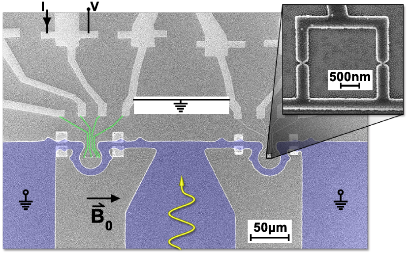
The device is etched from a 20 nm thin film of Nb to allow its operation in static magnetic fields parallel to the film. The Nb is sputtered on a Si chip coated with 300 nm SiO2. A broadband 50 coplanar waveguide is fabricated using ultra-violet lithography. The coplanar waveguide sends the microwave excitation into a central line of width 150 \textmugreekm, which is narrowed at the end and terminated with two shortcircuits shaped like letter , with internal radius of 15 \textmugreekm, towards the lateral ground planes as shown in Fig. 1. The micro-SQUIDs are fabricated in the middle of the -loops by means of electron beam lithography. The SQUID loop is 2.2 \textmugreekm 2.2 \textmugreekm with two Dayem bridge Josephson junctionsAnderson and Dayem (1964) of size 100 nm100 nm (see Fig. 1 inset). The middle wires provide the ground for all SQUIDs (see the horizontal line in the inset). Each loop contains three SQUIDs and each one can be individually read using the current-voltage line indicated in Fig. 1.
With this device, microwave pulses can generate a B-field component perpendicular to the chip plane in the middle of the -loop. In absence of a SQUID detector in the -loop, the waveguide is a 50 broadband device. By inserting a SQUID, an inductive coupling with the -loop allows the microwave energy to drain into the SQUID. This induces a cavity effect with a strong mode defined by the length of the patterned waveguide and with regions of maximum B-field at its ends. One can thus place a sample containing a small number of spins atop of the loop, to be excited by the microwave field. By using an external superconducting coil, a magnetic field is applied to SQUID plane. Such a planar field provides the desired Zeeman splitting for the spins while leaves the SQUID almost unaffected.
The functioning principle of a dc-SQUID is based on the well-known modulation of its switching current as a function of flux penetrating its loop, which has a period of one flux quanta with Planck’s constant and the electron charge.
The switching current is measured by monitoring the presence (switch event) or absence (non-switch event) of voltage pulses when a current pulse is injected in the SQUID (see the and lines in Fig. 1). The percentage of switching events defines the switching probabilityChiorescu et al. (2003) . A weak-link SQUID has a reduced depth of modulation, compared to a tunnel junction SQUID but can work under very large static fields. Fig. 2 shows the at K as a function of the current pulse height (vertical axis) and magnetic flux (horizontal axis). The switching current is sharply defined as the pulse height such that , at the transition between the regions (dark blue) and 1 (light blue). The modulation allows the detection of a signal coming from a magnetic sample.
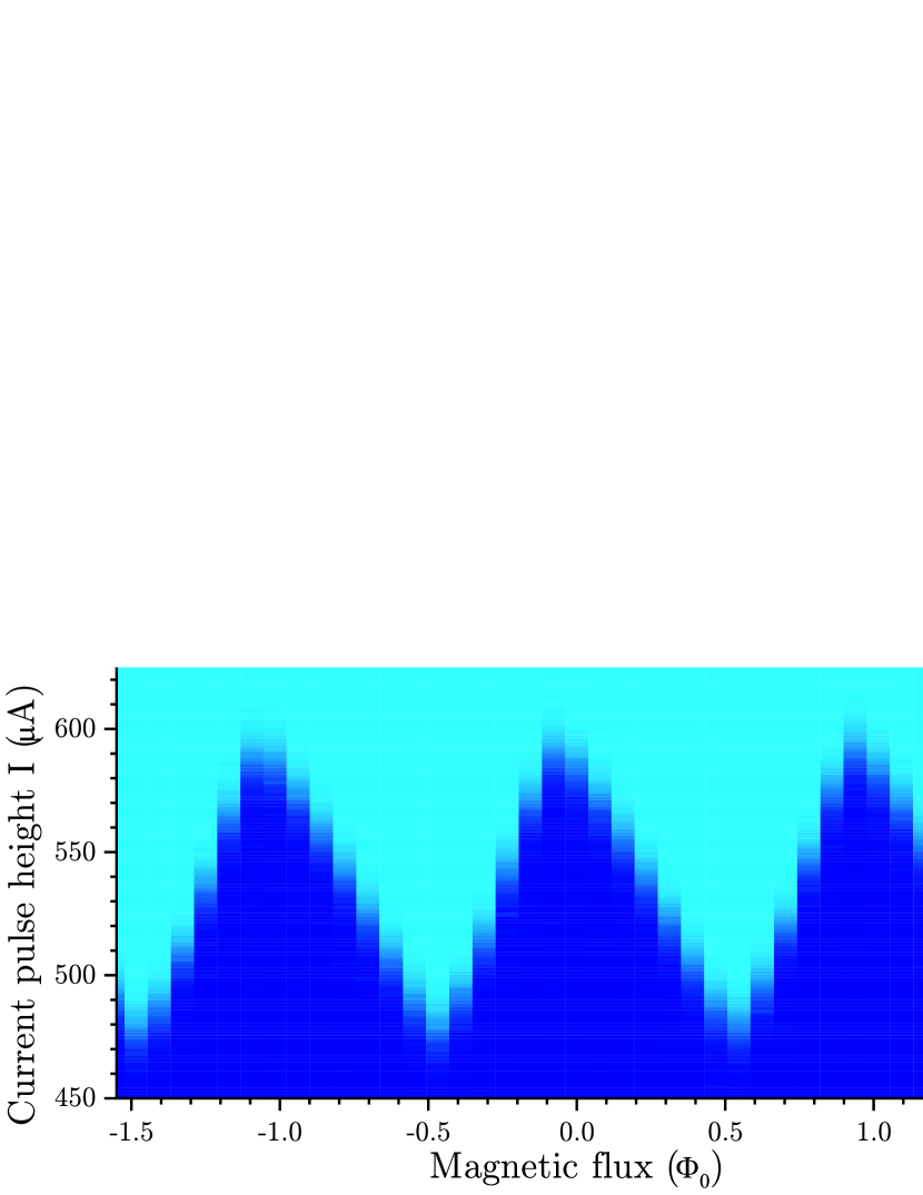
The switching probability is also highly sensitive to the presence of microwave radiation. When the SQUID is biased with a current pulse close to , microwave radiation can excite the SQUID and thus generate a switching event, similar to a thermal activation process Clarke and Braginski (2006); Lefevre-Seguin et al. (1992). One can therefore use the micro-SQUID as both magnetic flux and microwave detector, to detect magnetization changes, the usual case of magnetometers, or microwave emission of spins, as in traditional ESR, respectively. If the magnetic flux change is larger than , a feedback coil can be used to fix the SQUID’s working point and track the change of Wernsdorfer and Sessoli (1999); Chen et al. (2010). Here, the flux changes due to spin excitations are expected to be very small and the working point location in the plot of Fig. 2 is essentially fixed by a normal static field arrising from an imperfect field alignement in the SQUID plan.
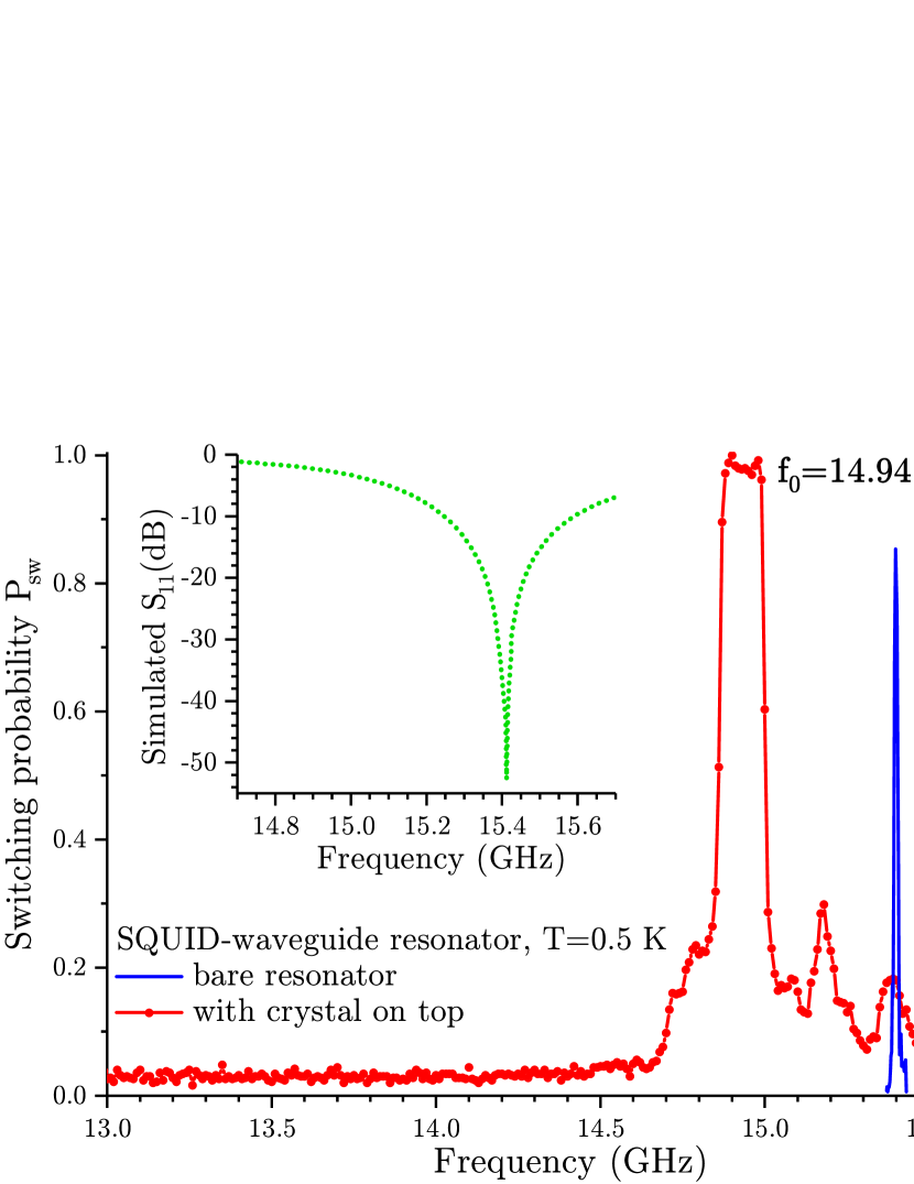
To verify the design, the SQUID is measured at 0.5 K under microwave excitation as a function of frequency, with and without a crystal of Gd-doped CaWO4 placed on top of the chip. The CaWO4 has a permitivittyKim, Kim, and Lee (2006) and therefore a shift of the resonance frequency is to be expected when the crystal is placed on top of the chip. The blue line in Fig. 3 shows the SQUID response in the case of an unloaded resonator with an estimated power at the chip entrance of dBm. Given the large amount of power, the bias current has a low value of 45 \textmugreekA, which allows to select the fundamental resonance at 15.4 GHz. The red dots show for a loaded cavity and indicate a resonance shift to GHz. To show the versatility of the device, in the loaded case, the power is reduced by 35 dB, which allows to operate at a higher bias current (329 \textmugreekA). Outside the resonance, there are very few switching events () likely due to thermal activation. Under these conditions, other very low intensity modes are observed above 15 GHz. One notes that the SQUID is not shunted by a designated capacitance, the modes are independent on bias and at a temperature of 0.5 K one cannot observe SQUID’s internal level structure. During the ESR experiment, the microwave frequency is fixed at the main mode GHz and the external field can tune the spins in and out of resonance. The resonance is sufficiently broad to neglect in-plane field and microwave power induced shifts.
To confirm the cavity effect we have performed finite element simulations in COMSOL, in which we discretized the structure of the chip numerically and computed the values of the S-parameters as a function of frequency. The SQUID was simulated as a COMSOL lumped port defined between the -loop and the ground metallic plane on which the Si chip is fixed. The port impedance defines the amount of absorbed energy and thus the resonance effect inside the waveguide structure. For the physical dimensions of the current device, the optimal value is . The corresponding simulated frequency dependence of is given in Fig. 3 (inset) and it shows a clear resonance at 15.4 GHz.
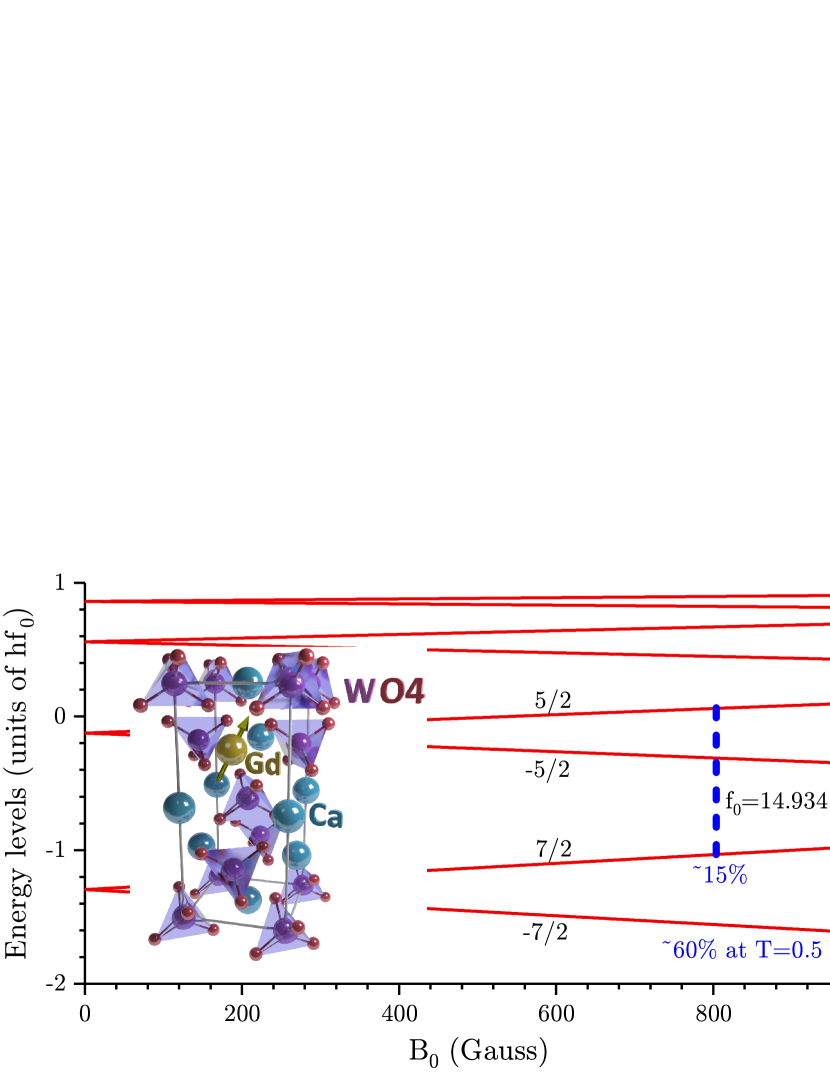
The spin Hamiltonian for the Gd3+ ions diluted in CaWO4 (tetragonal symmetry , see inset of Fig. 4) is the followingBaibekov et al. (2017):
| (1) |
where is magnetic field along the crystallographic -axis, are Stevens operatorsStevens (1952), is Bohr magneton, is the g-factor along the axis, and the crystal field parameters are (in units of MHz) and . has a detectable temperature dependenceHarvey and Kiefte (1971). Instead of a valueBaibekov et al. (2017) of MHz at 293 K, our data indicates that at 0.5 K, its value should be MHz. The obtained eigenvalues of are shown in Fig. 4; the blue dashed line indicates the field location of the resonance , at G. The shift in frequency caused by the loading of the resonator is larger than our expectations and no ground-state transitions fell within the appropiate experimental conditions. However, it is noteworthy that a successful measurement of such excited transition is relevant to show both the high sensitivity of the device as well as the potential of performing coherence control of multiple levels using this resonator and detection system.
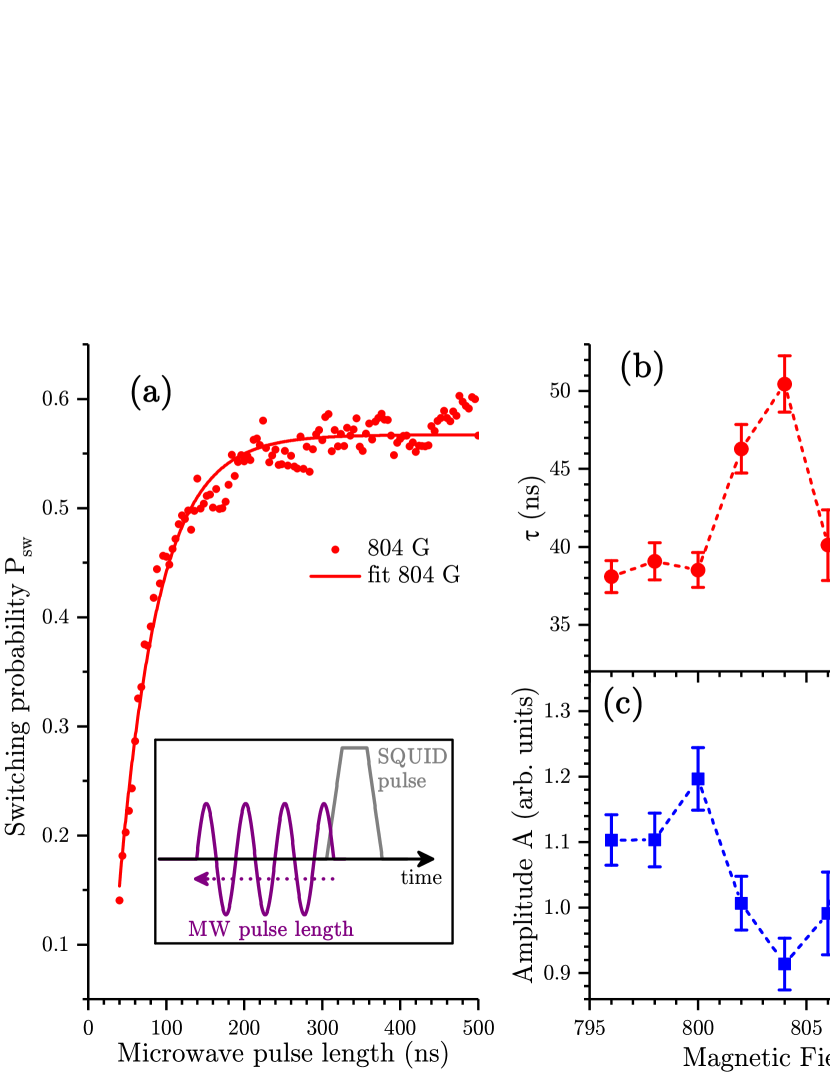
At 6 K, the Gd spins have a typical relaxation timeBaibekov et al. (2017) of the order of 10 ms and likely larger at our operating temperature of 0.5 K. Consequently the repetition frequency of the current pulse is decreased to 40 Hz to allow some amount of relaxation between consecutive measurements. The microwave excitation can be applied in either CW or pulsed modeChiorescu et al. (2003). The end point of the microwave pulse is chosen such that it barely overlaps with the micro-SQUID readout pulse, as sketched in the inset of Fig. 5(a). In this way, the SQUID can detect flux changes due to spin rotation as well as energy absorption without saturating the SQUID readout. Once the overlap is fixed, the length of the microwave pulse can be varied by changing its start time, as indicated with a dashed left-arrow. For each length, the value of is obtained by repeating the shown pulses for 3,000 times and recording the percentage of SQUID switching events. The current SQUID pulse is fixed at \textmugreekA and 2.1 \textmugreeks.
A single crystal of Gd-doped CaWO4 with dimensions of 0.63 mm 2.4 mm 0.95 mm was placed over both shortcircuits shown in Fig. 1 such that the external magnetic field is parallel to its -axis (also -axis) with a precision of . Using dedicated direct-current and high frequency electronics, the SQUID switching probability can be recorded as a function of temperature, magnetic field and microwave pulse characteristics. At K, frequency and power dBm, Fig. 5(a) shows vs. microwave pulse length at the resonance field G. As increases, the amount of energy pumped in the SQUID increases and therefore increases up to a saturation level reached around ns. The data is fitted with function where and are fit parameters, as shown in Fig. 5(a) with a continous line. The measurements are repeated with a 2 G step in the resonance region and the obtained and parameters and their uncertainties are shown in Fig. 5(b) and (c).
At the resonance field 804 G, the characteristic time has a peak, while has a dip, which are due to the absorption of energy by resonant spins (slower saturation towards a smaller plateau). This indicates the resonant absorption of microwave energy corresponding to the transition. The linewidth of the resonance signal is about 4 G or 25 MHz in frequency units, which is a typical value for diluted spin systems (decoherence time of the entire spin ensemble 40 ns). Spin-echo detection and Rabi oscillations at higher microwave powers are needed to characterize the decoherence time. The SQUID-waveguide device discussed here does offer the flexibility needed for such future studies.
The microwave pulse can excite only the spins situated in the very close proximity of the chip surface. The numerical simulations show that the microwave field inside the -loop decays fast with height: from a surface value of 0.15 G (corresponding to an estimated -10 dBm input power in our experiments), the field halves at 11 \textmugreekm above the chip. Due to the \textmugreekm size of the SQUID and the fast decay of the microwave field, the effective detected sample volume is estimated as in Ref. [Toida et al., 2016] to be \textmugreekm3 size, which corresponds to spins in the case of the CaWO4:Gd3+ sample discussed here.
To perform Rabi oscillations with well-defined nutation rates, it is important to have an homogenous microwave field in the sample. This can be achieved by using very thin samples, which can be prepared, for instance, by chemical growth in 2D configurations, using radiation to generate defects or by cuting ultra-thin samples using a focused ion beam. Typical decoherence times in diluted spin systems are of the order of \textmugreeksBaibekov et al. (2017); Bertaina et al. (2009), requiring Rabi frequencies of MHz and microwave fields of several Gauss. Such values are attainable in future implementations of the technique presented here, by using higher microwave pulsed fields while operating the SQUID in its classical regime ( K). It is expected that the signal size will actually increase due to population inversion generated by full spin rotation.
We present a sensitive on-chip detection scheme able to measure the first excited transition in a multi-level quantum spin system, at low temperatures. Gd spins diluted in a CaWO4 crystal are in resonance with the microwave excitation contained in a small volume around an -shaped shortcircuit. A rough estimation of the number of detected spins is . This SQUID-based resonator can be used in future studies to perform gated control of spin rotations.
This work was supported by the NSF Grant No. DMR-1206267 and CNRS-PICS CoDyLow. The NHMFL is supported by the Cooperative Agreement Grant No. DMR-1157490 and the State of Florida. We acknowledge support from the Strategic Priority Research Program of the Chinese Academy of Sciences (Grant No. XDB04000000). We are thankful to Dr. A. Tkachuk for providing the Gd sample and to X. Lian, S. Zhang and Dr. Xiong for the support in device fabrication.
References
- Morton and Lovett (2011) J. J. L. Morton and B. W. Lovett, Annual Review of Condensed Matter Physics 2, 189 (2011).
- Gershenfeld and Chuang (1997) N. A. Gershenfeld and I. L. Chuang, Science 275, 350 (1997).
- Bertaina et al. (2008) S. Bertaina, S. Gambarelli, T. Mitra, B. Tsukerblat, A. Müller, and B. Barbara, Nature 453, 203 (2008).
- Ardavan et al. (2007) A. Ardavan, O. Rival, J. J. L. Morton, S. J. Blundell, A. M. Tyryshkin, G. A. Timco, and R. E. P. Winpenny, Physical Review Letters 98, 057201 (2007).
- Shiddiq et al. (2016) M. Shiddiq, D. Komijani, Y. Duan, A. Gaita-Ariño, E. Coronado, and S. Hill, Nature 531, 348 (2016).
- Bader et al. (2014) K. Bader, D. Dengler, S. Lenz, B. Endeward, S.-D. Jiang, P. Neugebauer, and J. van Slageren, Nature Communications 5, 5304 (2014).
- Jelezko et al. (2004) F. Jelezko, T. Gaebel, I. Popa, M. Domhan, A. Gruber, and J. Wrachtrup, Physical Review Letters 93, 130501 (2004).
- Bertaina et al. (2007) S. Bertaina, S. Gambarelli, A. Tkachuk, I. N. Kurkin, B. Malkin, A. Stepanov, and B. Barbara, Nature Nanotechnology 2, 39 (2007).
- Bertaina et al. (2009) S. Bertaina, L. Chen, N. Groll, J. Van Tol, N. S. Dalal, and I. Chiorescu, Physical Review Letters 102, 050501 (2009).
- Nellutla et al. (2007) S. Nellutla, K.-Y. Choi, M. Pati, J. van Tol, I. Chiorescu, and N. S. Dalal, Physical Review Letters 99, 137601 (2007).
- Baibekov et al. (2017) E. I. Baibekov, M. R. Gafurov, D. G. Zverev, I. N. Kurkin, A. A. Rodionov, B. Z. Malkin, and B. Barbara, Physical Review B 95, 064427 (2017).
- Leuenberger and Loss (2001) M. N. Leuenberger and D. Loss, Nature 410, 789 (2001).
- Blencowe (2010) M. Blencowe, Nature 468, 44 (2010).
- Chiorescu et al. (2010) I. Chiorescu, N. Groll, S. Bertaina, T. Mori, and S. Miyashita, Physical Review B 82, 024413 (2010).
- Schuster et al. (2010) D. I. Schuster, A. P. Sears, E. Ginossar, L. DiCarlo, L. Frunzio, J. J. L. Morton, H. Wu, G. A. D. Briggs, B. B. Buckley, D. D. Awschalom, and R. J. Schoelkopf, Physical Review Letters 105, 140501 (2010).
- Wu et al. (2010) H. Wu, R. E. George, J. H. Wesenberg, K. Mølmer, D. I. Schuster, R. J. Schoelkopf, K. M. Itoh, A. Ardavan, J. J. L. Morton, and G. A. D. Briggs, Physical Review Letters 105, 140503 (2010).
- Saito et al. (2013) S. Saito, X. Zhu, R. Amsüss, Y. Matsuzaki, K. Kakuyanagi, T. Shimo-Oka, N. Mizuochi, K. Nemoto, W. J. Munro, and K. Semba, Physical Review Letters 111, 107008 (2013).
- Bienfait et al. (2016) A. Bienfait, J. J. Pla, Y. Kubo, M. Stern, X. Zhou, C. C. Lo, C. D. Weis, T. Schenkel, M. L. W. Thewalt, D. Vion, D. Esteve, B. Julsgaard, K. Mølmer, J. J. L. Morton, and P. Bertet, Nature Nanotechnology 11, 253 (2016).
- Abeywardana et al. (2016) C. Abeywardana, V. Stepanov, F. H. Cho, and S. Takahashi, Journal of Applied Physics 120, 123907 (2016).
- Antler et al. (2013) N. Antler, E. M. Levenson-Falk, R. Naik, Y.-D. Sun, A. Narla, R. Vijay, and I. Siddiqi, Applied Physics Letters 102, 232602 (2013).
- Sigillito et al. (2014) A. J. Sigillito, H. Malissa, A. M. Tyryshkin, H. Riemann, N. V. Abrosimov, P. Becker, H.-J. Pohl, M. L. W. Thewalt, K. M. Itoh, J. J. L. Morton, A. A. Houck, D. I. Schuster, and S. A. Lyon, Applied Physics Letters 104, 222407 (2014).
- Baumann et al. (2015) S. Baumann, W. Paul, T. Choi, C. P. Lutz, A. Ardavan, and A. J. Heinrich, Science 350, 417 (2015).
- Artzi, Twig, and Blank (2015) Y. Artzi, Y. Twig, and A. Blank, Applied Physics Letters 106, 084104 (2015).
- Wernsdorfer et al. (1997) W. Wernsdorfer, E. Bonet Orozco, K. Hasselbach, A. Benoit, D. Mailly, O. Kubo, H. Nakano, and B. Barbara, Physical Review Letters 79, 4014 (1997).
- Wernsdorfer et al. (2004) W. Wernsdorfer, A. Müller, D. Mailly, and B. Barbara, Europhysics Letters 66, 861 (2004).
- Cage et al. (2005) B. Cage, S. E. Russek, D. Zipse, J. M. North, and N. S. Dalal, Applied Physics Letters 87, 082501 (2005).
- Toida et al. (2016) H. Toida, Y. Matsuzaki, K. Kakuyanagi, X. Zhu, W. J. Munro, K. Nemoto, H. Yamaguchi, and S. Saito, Applied Physics Letters 108, 052601 (2016).
- Wernsdorfer and Sessoli (1999) W. Wernsdorfer and R. Sessoli, Science 284, 133 (1999).
- Chen et al. (2010) L. Chen, W. Wernsdorfer, C. Lampropoulos, G. Christou, and I. Chiorescu, Nanotechnology 21, 405504 (2010).
- Chen et al. (2016) L. Chen, H. Wang, X. Liu, L. Wu, and Z. Wang, Nano Letters 16, 7726 (2016).
- Anderson and Dayem (1964) P. W. Anderson and A. H. Dayem, Physical Review Letters 13, 195 (1964).
- Chiorescu et al. (2003) I. Chiorescu, Y. Nakamura, C. J. P. M. Harmans, and J. E. Mooij, Science 299, 1869 (2003).
- Clarke and Braginski (2006) J. Clarke and A. Braginski, eds., The SQUID Handbook, Vol. 1 (Wiley-VCH Verlag GmbH & Co. KGaA, 2006) p. 409.
- Lefevre-Seguin et al. (1992) V. Lefevre-Seguin, E. Turlot, C. Urbina, D. Esteve, and M. H. Devoret, Physical Review B 46, 5507 (1992).
- Kim, Kim, and Lee (2006) E. S. Kim, S. H. Kim, and B. I. Lee, Journal of the European Ceramic Society 26, 2101 (2006).
- Stevens (1952) K. W. H. Stevens, Proceedings of the Physical Society. Section A 65, 209 (1952).
- Harvey and Kiefte (1971) J. S. M. Harvey and H. Kiefte, Canadian Journal of Physics 49, 995 (1971).