Edge magnetism impact on electrical conductance and thermoelectric properties of graphenelike nanoribbons
Abstract
Edge states in narrow quasi two-dimensional nanostructures determine, to a large extent, their electric, thermoelectric and magnetic properties. Non-magnetic edge states may quite often lead to topological insulator type behavior. However another scenario develops when the zigzag edges are magnetic and the time reversal symmetry is broken. In this work we report on the electronic band structure modifications, electrical conductance and thermoelectric properties of narrow zigzag nanoribbons with spontaneously magnetized edges. Theoretical studies based on the Kane-Mele-Hubbard tight-binding model show that for silicene, germanene and stanene both the Seebeck coefficient and the thermoelectric power factor are strongly enhanced for energies close to the charge neutrality point. Perpendicular gate voltage lifts the spin degeneracy of energy bands in the ground state with antiparallel magnetized zigzag edges and makes the electrical conductance significantly spin-polarized. Simultaneously the gate voltage worsens the thermoelectric performance. Estimated room-temperature figures of merit for the aforementioned nanoribbons can exceed a value of 3 if phonon thermal conductances are adequately reduced.
pacs:
73.63.Kv,72.25.-b,73.50.LwI Introduction
Recently there has been enormous interest in the physical properties of graphene nanostructures and other similar quasi two-dimensional systems. It is believed that these systems will soon enter the field of modern nanoelectronics, including spintronics and calorytronics. Here we study the latter two issues. The question how to improve the thermoelectric performance of nanostructures has been addressed in many scientific reports. It is worth mentioning in this context the following methods aimed at achieving this purpose: shape and grain boundary manipulations [Sevi12, ; TUDPRB15, ], energy spectrum engineering [Karamitaheri12, ; Zheng15, ], and magnetism-related concepts based on magnetic proximity effects coming from substrates (staggered magnetization) and the impact of the external magnetic field [Wierzb15, ]. The existence of edge magnetism in the case of narrow high quality graphene nonoribbons is now well documented [Joly10, ; Tao11, ; Gao13, ; Magda14, ; Li14, ]. It is very probable that similar evidences in support of edge magnetism in other graphenelike nanostructures will also be demonstrated soon. The best known graphenelike nanostructures (e.g. silicene, germanene and stanene) are quasi two-dimensional rather than strictly 2-dimensional because their sublattices are shifted with respect to each other by the so-called buckling distance in the off-plane direction [Guzman2007, ; Cahangirov2009, ; Liu2011, ; Kamal2015, ; Ezawa2015, ; Gomez16, ]. In contrast to graphene the buckled structures usually have a non-negligible intrinsic spin-orbit coupling which strongly influences their electronic energy band structures and physical properties of interest here.
II Model and Methodology
In order to catch the essential physics of graphenelike nanoribbons (GLNRs) we use a tight-binding Hamiltonian with Hubbard-type electron correlations, intrinsic spin-orbit interaction (ISOI), and an extra term describing the effect of the gate voltage applied in a perpendicular way. Noteworthily, the presence of the ISOI introduces anisotropy, so it is necessary to include in the Hubbard part of the Hamiltonian both the spin diagonal correlations and the off-diagonal ones. The total Hamiltonian reads:
| (1) | |||||
with
| (2) |
| (3) |
| (4) |
In Eq. (2) the summation runs over the next nearest-neighbors, and the factor , depending on whether the path from i to j is clockwise or counterclockwise. The factor , in turn, equals 1 (-1) for sublattice A (B). Other symbols have the following meaning: is the hopping integral, is the intraatomic Coulomb repulsion, corresponds to the in-plane (out-of-plane) configuration, are annihilation (creation) operators, and and stand for a lattice site and spin, respectively, whereas and , . Angular brackets stand for expectation values over the ground state, and
| (5) |
| (6) |
| (7) |
The electronic band structure is determined from the eigenequation
| (8) |
where the matrix describes coupling between 2 neighboring super-cells (as shown in Fig.1). Explicitly for 8 atoms in the super-cell:
| (9) |
with , , and (nearest neighbor hopping).
In order to determine which of the possible configurations constitutes the ground state, grand canonical potentials are computed from the following expression (with a correction due to the last terms in Eqs. II)
| (10) |
The configurations in question are those with in-plane (IN) or out-of-plane (OUT) magnetization arrangements, and parallel (P) or antiparallel (AP), respectively, magnetic orientations of the opposite zigzag edges (abbreviations: In-AP, Out-AP, IN-P and OUT-P).
III Electronic band structure and edge magnetic moments
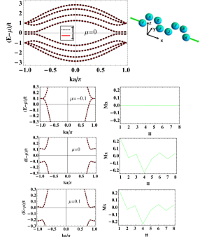
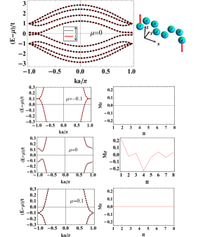
Studies of nanoribbons with magnetic moments are computationally much more demanding than those corresponding to nonmagnetic ones [SK11, ]. This is so because magnetic moments, and thereby also electronic band structures, depend strongly on the chemical potential position. Hence, for each the band structure has to be determined again and again. This is visualized in Figs 2 and 3, which show that bands in the vicinity of the K and K’ points differ from one another depending on whether magnetic moments do or do not exist. Moreover it is readily seen that on the one hand in the Out-AP case the energy spectrum may be valley-polarized (different energy gaps at K and K’ points) and on the other hand the edge magnetism disappears with increasing earlier in that case than in the In-AP configuration (cf magnetization profiles for ). Incidentally, in the case of graphene there is neither ISOI nor magnetic anisotropy, that is why the configurations IN and OUT are equivalent.
Theoretical studies of graphenelike nanoribbons are usually carried out for the out-of-plane configuration [Soriano10, ; Lu14, ], but it is now known that the in-plane configuration is often energetically the most stable one [Lado2014, ; WBK2015, ; SKNanotech2016, ]. Here most of our attention is directed to this very configuration which constitutes the ground state for energies close to the charge neutrality point (CNP).
IV Electronic transport and thermoelectric performance
The following standard relations are used for the electrical conductance, Seebeck coefficient and electronic heat conductance (Ref. [Karamitaheri12, ] and references therein):
| (11) |
Above and are fundamental physical constants, and T denotes the temperature. G, S, stand for the conductance, Seebeck coefficient and electronic thermal conductance (with corresponding units in brackets), respectively. is the (ballistic) transmission matrix equal to the number of forward propagating modes. Finally, is the Fermi-Dirac distribution function, and denotes the chemical potential. The temperature is set equal to 300K, in view of the fact that room temperature magnetic order on zigzag edges of narrow nanoribbons has been recently reported [Magda14, ].
Other quantities of interest here are thermoelectric power factor and figure of merit and , respectively.
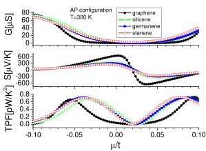
We have performed comparative calculations for graphene, silicene, germanene and stanene using sets of parameters according to [Ezawa2015, ]. It should be noted that apart from graphene these materials possess finite and buckling parameters and have comparable lattice constants (a) and hopping integrals (t). The latter two parameters for graphene differ considerably from those for the other graphenelike materials. This is why the results for silicene, germanene and stanene differ less from one another than from those for graphene. This is clearly visible in Figs. 4. In the IN-AP configuration and at 300K both TPFs and Seebeck coefficients always have pronounced extrema in the vicinity of the charge neutrality point. The conductances (G) close to the CNP, in turn, are nearly zero because, as shown in Fig.2, the systems have nonzero energy gaps. Of course at elevated temperatures the gap effects get strongly reduced and smeared. The results for G, S and TPF in the case of graphene are similar to those reported in [Karamitaheri12, ] where a significant enhancement of the thermoelectric performance was achieved by introducing extended line defects (ELD). It follows from this comparison that the enhancement of the Seebeck coefficient due to edge magnetism might outperform that due to the ELD by a factor of 2, whereas the TPFs are roughly the same. Similar conclusions result from an analogous comparison of the S-factor with that from [Zheng15, ] where the enhancement comes from the application of ferromagnetic leads and gating of the central region (germanene nanoribbon).
IV.1 Figure of merit
As concerns figures of merit, following the practice of other authors, we assume that the phonon thermal conductance () may be substantially suppressed mainly by substrates, structural imperfections, defects and isotopic inhomogeneities [Seol2010, ; Zheng15, ; gunstPRB11, ; Wierzb15, ; TUDPRB15, ; Sevi12, ]. Because this type of effects is not explicitly included in the present theory, is replaced by with the scaling factor ().gunstPRB11 ; Zberecki2013 Suppressions corresponding to and in graphene were measured in [Seol2010, ] and predicted theoretically in [Sevi12, ], respectively. The former result was due to the effect of a substrate, whereas the latter was found via a combination of geometrical structuring and isotope engineering. Moreover, a 100-fold reduction in thermal conductivity was also measured in rough silicon nanowires.Hochbaum08
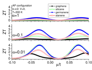
The -values for all systems studied here were taken from Ref. [Peng2016, ]. Figure 5 shows that in the case of (no phonon suppression) only germanene has ZT nearly equal to 1, but with decreasing the graphenelike nanostructures reveal quite high ZT-values. In particular, silicene, germanene and stanene have relatively large ZT factors attractive from the point of view of potential practical applications provided their phonon thermal conductances are reduced by 90% or more. In fact, systems with are already regarded as good thermoelectric materials, and those having would be competitive with the best of the conventional energy conversion devices. gunstPRB11 However it should be kept in mind that experimental realization of the GLNRs of interest here is a big challenge, although at present good-quality nanoribbons of the necessary chirality can be fabricated, Tang13 ; Magda14 ; Li14 and advanced experimental techniques for electrical and thermal transport measurements are very well developed.Bauer12 ; Lee12 ; Xu14
The present findings show that the existence of edge magnetism improves the electrical performance of the GLNRs. On the one hand graphene which is known to be an inefficient thermoelectrical material [Balendhran2015, ], according to the present theory has ZT close to 1.5 (Fig.5, bottom panel). On the other hand our results for silicene and germanene are consistent with those in [Yang14, ] (and in [Hochbaum08, ] for Si nanowires) for ; moreover the ZT values still increase rapidly with further decreasing .
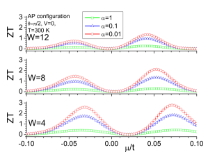
So far the case of ultra narrow (4 atom wide) infinitely long graphenelike nanoribbons has been considered in detail. This case corresponds to the width of ca. 1nm (accessible experimentally [Magda14, ; Li14, ]). The results for ZT coefficients as a function of the nanoribbon width, presented in Fig. 6, show that with increasing width the enhancement of thermoelectric characteristics becomes less and less pronounced. Noteworthily, in the case of stanene 12 zigzag lines in width (roughly 5 nm) the maximum value of ZT is still slightly above 1. From the experimental side it is known [Magda14, ]) that for 7 8 nm wide graphene nanoribbons the energy gap collapses, which, according to the present theory, implies drastic worsening of thermoelectric properties.
IV.2 Gate voltage effect
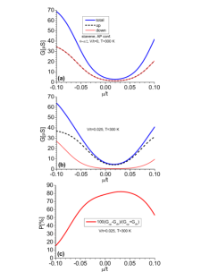
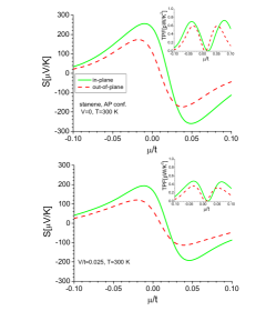
The gate voltage effect has been intensively studied by many authors.Drummond2012 ; Ezawa2015 ; Tsai2013 If there is no edge magnetism, a small ISOI-induced energy gap gets closed for . The case of graphenelike nanoflakes with magnetic edges has been studied in Ref. [SKNanotech2016, ] and it has been found that then the critical is substantially increased. Here, as an example, V/t has been set equal to 0.025 for stanene, so as to guarantee a significant spin splitting without suppressing of the edge magnetism. In the absence of any vertical gate voltage the electrical conductances are not spin-split in the AP arrangement (Fig.7(a)), but the degeneracy is lifted at finite (panel (b)) resulting in the achievement of a relative spin-polarization of more than 80% (panel (c)). Unfortunately, a similar trick is not possible for a graphene monolayer since then the A and B sublattice atoms are coplanar and there is no way to gate them independently. As regards the thermoelectric properties, the Seebeck coefficients (S) and the TPFs are the biggest in the case of the in-plane configuration. Moreover, as clearly shown in Fig.8, in the presence of a finite gate voltage the thermoelectric performance slightly worsens. Additionally, it should be emphasized that in the case of systems with no band gap, i.e. with parallel alignment of edge magnetizations, or non-magnetic edges, the thermoelectric performance is extremely poor.
V Summary
In this paper we have analyzed the impact of the edge magnetism on the electrical transport and thermoelectric properties of selected graphenelike nanoribbons (silicene, germanene, stanene, plus graphene for comparison). It has been found that the ground state of these nanoribbons corresponds to the IN-AP magnetic configuration, i.e. the in-plane antiparallel arrangement of edge magnetic moments. Close to the charge neutrality point (CNP) the systems are small gap semiconductors at low temperatures. At room temperature both the Seebeck coefficient and the thermopower factor reveal high peaks for energies in the vicinity of the CNP. The same applies to the ZT factors whose values can exceed 3 provided that their phonon thermal conductance is appropriately reduced. As concerns the perpendicular gate voltage, its effect is quite promising for possible spintronic applications connected with spin-polarized current (cf. [Tsai2013, ]).
Acknowledgements.
This project was supported by the Polish National Science Centre from funds awarded through the decision No. DEC-2013/10/M/ST3/00488.References
- (1) Lehmann T, Ryndyk D A and Cuniberti G 2015 Phys. Rev. B 92 035418
- (2) Sevinçli H, Sevik C, Çaǧin T and Cuniberti G 2013 Scientific Reports 3 1228
- (3) Karamitaheri H, Neophytou N, Pourfath M, Faez R and Kosina H 2012 J. Appl. Phys. 111 054501
- (4) Zheng J, Chi F and Guo Y 2015 J. Phys.: Condens. Matter 27 295302
- (5) Wierzbicki M, Barnaś J and Świrkowicz R 2015 Phys. Rev. B 91 165417
- (6) Joly V L J, Kiguchi M, Hao S J, Takai K, Enoki T, Sumii R, Amemiya K, Muramatsu H, Hayashi T, Kim Y A, Endo M, Campos-Delgado J, López-Urías F, Botello-Méndez A, Terrones H and Terrones M 2010 Phys. Rev. B 81 245428
- (7) Gao D, Si M, Li J, Zhang J, Zhang Z, Yang Z and Xue D 2013 Nanoscale Res. Lett. 8 129
- (8) Tao C, Jiao L, Yazyev O V, Chen Y C, Feng J, Zhang X, Capaz R B, Tour J M, Zettl A, Louie S G, Dai H and Crommie M F 2011 Nat. Phys. 7 616
- (9) Magda G Z, Jin X, Hagymasi I, Vancso P , Osvath Z, Nemes-Incze P, Hwang C, Biro P P and Tapaszto L 2014 Nature 514 608
- (10) Li Y Y, Chen M X, Weinert M and Li L 2014 Nat. Commun. 5, 4311
- (11) Guzmán-Verri G G, Lew Yan Voon L C 2007 Phys. Rev. B 76 075131
- (12) Cahangirov S, Topsakal M, Akturk E, Sahin H and Ciraci S 2009 Phys.Rev. Lett. 102 236804
- (13) Liu C -C, Jiang H and Yao Y 2011 Phys. Rev. B 84, 195430
- (14) Kamal C, Chakrabarti A and Ezawa M 2015 New J. Phys. 17 083014
- (15) Ezawa M 2015 J. Phys. Soc. Jap. 84 121003
- (16) Castellanos-Gomez A 2016 Nat. Phot. 10 202
- (17) Krompiewski S 2011 Nanotechnology 22 445201
- (18) Soriano D and Fernández-Rossier J 2010 Phys. Rev. B 82 161302
- (19) Lu Y, Zhao S, Zhang Y, Liu H, Lu W and Liang W 2014 Mater. Res. Express 1 045009
- (20) J. L. Lado J L and Fernández-Rossier J 2014 Phys. Rev. Lett. 113 027203
- (21) Weymann I, Barnaś J and Krompiewski S 2015 Phys. Rev. B 92 045427
- (22) Krompiewski S 2016 Nanotechnology 27 315201
- (23) Gunst T, Markussen T, Jauho A P and Brandbyge M 2011 Phys. Rev.B 84 155449
- (24) Seol J H, Jo I, Moore A L, Lindsay L, Aitken Z H, Pettes M T, Li X, Yao Z, Huang R and Broido D, 2010 Science 328 213
- (25) Zberecki K, Wierzbicki M, Barnaś J and Świrkowicz R 2013 Phys. Rev. B 88, 115404
- (26) Hochbaum A I, Chen R, Delgado R D, Liang W, Garnett E C, Najarian M, Majumdar A and Yang P, 2008 Nature 451 163
- (27) Peng Bo, Zhang Hao, Shao Hezhu, Xu Yuanfeng, Ni Gang, Zhang Rongjun, and Zhu Heyuan 2016 Phys. Rev. B, 94 245420
- (28) Q. Tang and Z. Zhou, Prog. Mater. Sci. 58, 1244 (2013).
- (29) G. E. W. Bauer, E. Saitoh, and B. J. van Wees, Nat. Mater. 11, 391 (2012).
- (30) E. K. Lee, L. Yin, Y. Lee, J. W. Lee, S. J. Lee, J. Lee, S. N. Cha, D. Whang, G. S. Hwang, K. Hippalgaonkar, A. Majumdar, C. Yu, B. L. Choi, J. M. Kim, and K. Kim, Nano Lett. 12, 2918 (2012).
- (31) Y. Xu , Z. Li , and W. Duan, Small, 10, 2182 (2014).
- (32) Balendhran S , Walia S, Nili H , Sriram S and Bhaskaran M 2015 small 11 640
- (33) Yang K, Cahangirov S, Cantarero A, Rubio A and D’Agosta R 2014 Phys. Rev. B, 89, 125403
- (34) Tsai W -F, Huang C -Y, Chang T -R, Lin H, Yeng H -T and Bansil A 2013 Nat. Commun. 4 1500
- (35) Drummond N D, Zólyomi V and Fal ko V I 2012 Phys. Rev. B 85 075423