Quantum confined Stark effect in a MoS2 monolayer van der Waals heterostructure
Abstract
The optics of dangling-bond-free van der Waals heterostructures containing transition metal dichalcogenides are dominated by excitons. A crucial property of a confined exciton is the quantum confined Stark effect (QCSE). Here, such a heterostructure is used to probe the QCSE by applying a uniform vertical electric field across a molybdenum disulfide (MoS2) monolayer. The photoluminescence emission energies of the neutral and charged excitons shift quadratically with the applied electric field provided the electron density remains constant, demonstrating that the exciton can be polarized. Stark shifts corresponding to about half the homogeneous linewidth were achieved. Neutral and charged exciton polarizabilities of and at relatively low electron density () have been extracted, respectively. These values are one order of magnitude lower than the previously reported values, but in line with theoretical calculations. The methodology presented here is versatile and can be applied to other semiconducting layered materials as well.
The recent emergence of optically-active layered semiconductors Mak et al. (2010); Splendiani et al. (2010), such as molybdenum disulfide (MoS2), and of the so-called van der Waals heterostructures (vdWhs) Geim and Grigorieva (2013); Novoselov et al. (2016) pave the way towards engineered quantum structures. Excitons in MoS2 and other transition metal dichalcogenides have particularly large exciton binding energies Chernikov et al. (2014) such that excitons dominate the optical properties, even at room temperature. Therefore, the fundamental properties of the excitons need to be elucidated. A basic feature of semiconductor nanostructures is the quantum confined Stark effect (QCSE), the change in optical response on applying an electric field perpendicular to the layers Miller et al. (1984). On the one hand, the QCSE characterizes the sensitivity of the exciton energy to charge noise as charge noise results in a fluctuating electric field within the device. The QCSE is therefore important in optimizing and understanding optical linewidths. On the other hand, the QCSE can be exploited to trap and manipulate excitons on the nano-scale by applying a locally varying vertical electric field High et al. (2008); Schinner et al. (2013).
When a DC electric field is applied perpendicular to a MoS2 monolayer (-axis), electrons and holes will tend to move apart in order to decrease their electrostatic potential energy. The resulting energy shift of the exciton energy is known as the QCSE and is given by where is the component of the electric field, the excitonic dipole moment and the excitonic polarizability along the -direction. Owing to the reflection symmetry about the molybdenum plane, in a MoS2 monolayer embedded in a symmetric dielectric environment Schuller et al. (2013) such that the QCSE is expected to be quadratic in .
Measurement of the Stark shift of the A-exciton in a MoS2 monolayer has been reported Klein et al. (2016). However, the experiment was performed on monolayers encapsulated in standard oxides (aluminium and silicon oxides) which have poor optical quality and, most probably, contain a significant density of charge traps Guo et al. (2015). Lately, a theoretical study Pedersen (2016) has predicted to be more than one order of magnitude below the reported experimental value. An unambiguous measure of the QCSE in MoS2 is therefore missing. A particular challenge is that the exciton energies depend strongly on the electron density in the MoS2 monolayer Chernikov et al. (2015). Furthermore, the description of the optical excitations in the high-density regime has a strong many-electron flavor: the quasi-particles are no longer the simple excitons Sidler et al. (2016); Efimkin and MacDonald (2017). These considerations mean that the QCSE should be measured at a low and constant electron density.
In this Letter, high quality MoS2 monolayers, obtained by encapsulation in hexagonal boron nitride (h-BN), are used to determine precisely the QCSE of the neutral X0 and negatively charged X- A-excitons. The photoluminescence (PL) spectra of these samples show narrow linewidths ( 8 meV), close to the ideal limit ( Cadiz et al. (2017)), allowing the X0 and X- to be identified unambiguously. Both spectral features shift when applying an electric field. However, at the same time, the ratio between the integrated intensities of X- and X0 varies. The change in this ratio signifies a change in the electron density which, in turn, shifts the emission energies. To separate carefully QCSE and doping contributions to the energy shifts, additional measurements were performed on a directly contacted MoS2 device. These measurements quantify precisely both the X- to X0 intensity ratio and the exciton energy shifts as a function of the electron density. We use this information to find a region in the encapsulated device where the electric field can be changed at a constant and relatively low electron density. In this region, we demonstrate a clear QCSE. We determine excitonic polarizabilities typically one order of magnitude smaller than the values reported in Ref. Klein et al., 2016 but in good agreement with calculations in Ref. Pedersen, 2016.
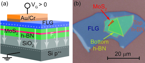
The QCSE was measured using the encapsulated device with geometry as depicted in Fig. 1(a): two thick h-BN layers are used as dielectric spacers and the top few-layer graphene (FLG) acts as a transparent electrode (see Methods for a description of the fabrication process). Applying a DC voltage between the FLG and the highly doped bottom Si substrate creates a uniform electric field in the MoS2 monolayer, oriented perpendicular to the basal plane of the sample. PL spectra were recorded at 4 K as a function of in a home-built confocal microscope (see Methods).

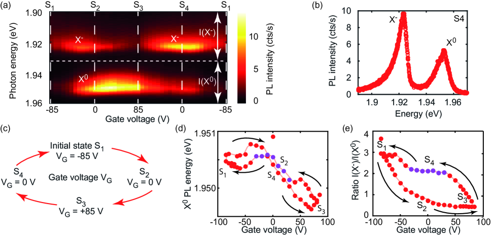
Figure 2(a) shows typical PL spectra recorded over a voltage loop as illustrated in Fig. 2(c): V varies from the initial state (S1) at V to V (S3) via S2 (0 V) and then back to S1 via S4 (0 V). Two prominent features can be clearly identified (see Fig. 2(b)): a low-energy peak near and a high-energy peak near attributed to the negatively charged X- and the neutral X0 A-excitons Mak et al. (2013); Cadiz et al. (2017), respectively. The emission energies of X- and X0 change with , as seen in Fig. 2(d) where the X0 energy has been plotted. However, as demonstrated in the colormap in Fig. 2(a), the intensities of the X- and X0 features also vary with . The ratio between the integrated PL intensities of X- and X0, (Fig. 2(e)), cannot be explained by the QCSE as it depends on the gate voltage sweep direction. Instead, the change in relative intensity arises from a change in the electron density Manassen et al. (1996).
In order to monitor the carrier density and its relation to , a reference sample consisting of an encapsulated yet contacted MoS2 monolayer was fabricated as sketched in the inset to Fig. 3(c). In this case, the MoS2 layer is directly contacted by a few-layer graphene sheet. This is a capacitive device and as such the electron density in the sample is expected to change linearly with the applied gate voltage Mak et al. (2013). This expectation was confirmed experimentally by measuring the energetic separation between the X0 and X- features in the PL spectra: we find a linear dependence of the X0 and X- energy separation with gate voltage (see Fig. 3(a)). At low electron densities, the energetic separation between X0 and X- scales linearly with the Fermi level, as ionization of X- requires that an electron is moved up to the Fermi level Hawrylak (1991); Mak et al. (2013). Given the linear dependence of Fermi energy on electron density for a two-dimensional system, the PL itself demonstrates that the reference sample charges as a capacitive device (with a capacitance ). It is noteworthy that the X0 and X- emission energies show opposite dependences on the electron density (Fig. 3(b)): X0 blue-shifts while X- red-shifts with increasing electron density Chernikov et al. (2015). As in the main sample, the reference sample shows hysteresis effects on ramping the voltage up and down due to photodoping from the surrounding h-BN Ju et al. (2014); Epping et al. (2016). The voltage at which the electron density is close to zero changes depending on the history of the device. However, we find a robust relationship between the intensity ratio and the X0, X- splitting, equivalently the electron density. Fig. 3(c) plots as a function of the electron density extracted from the PL spectra recorded at various gate voltages on the reference sample. This means that the ratio can be used as a measure of the electron density. The monotonic increase of this ratio with the electron density can be well described by a phenomenological exponential fit. This is used here as a calibration curve to evaluate the electron density in the main sample from the ratio.
Using the density calibration from the reference sample, the variation of the intensity ratio along the voltage loop displayed in Fig. 2(e) indicates a total variation of the electron density of in the main sample. This change in electron density when applying a gate voltage might arise as a combined consequence of photodoping effects Ju et al. (2014); Epping et al. (2016), tunneling Choi et al. (2013) from the FLG top gate through the insulating h-BN top layer, and charge trapping Wang et al. (2010) at the SiO2/h-BN interface. In order to isolate the QCSE contribution to the exciton energy, it is important to identify regions where the gate voltage can be swept without changing the ratio . Inspection of the data in Fig. 2(e) shows that there are no significant changes in MoS2 electron density around S3 and S4. These two regions are therefore good candidates for measuring the QCSE in MoS2.
Between S2 and S3, the ratio is small and corresponds to a region where MoS2 has a low electron density (). In this region, the X- signal is weak and evaluation of the ratio becomes unreliable. It is therefore difficult to attest that the Fermi level in this region remains absolutely constant. Moreover, it is in this range of Fermi energy that photo-induced doping from the h-BN layers occurs leaving charged defects in the h-BN that potentially induce electric field screening Ju et al. (2014). The region around S3 is therefore problematic with regards to the QCSE. The region around S4, between V and V, exhibits a stronger X- feature and the ratio can therefore be reliably measured. From this ratio, the electron density is evaluated to be in this region using the calibration curve displayed in Fig. 3(c) and remains constant to within 5%.
Fig. 4 displays the change in X- and X0 emission energies, and respectively, in the region around S4. was determined by dividing by the electrode-to-electrode distance of 300 nm and adding a constant built-in electric field of . This value was chosen such that and vanish at , i.e. it is assumed that . This built-in electric field arises from space charge within the layers of the heterostructure. Both and exhibit a quadratic dependence on , equivalently a linear dependence on , as shown in Fig. 4. This is the signature of a QCSE. We argue that the experiment reveals a QCSE and not a residual effect of any small changes in carrier density. First, for each point the measurement error in results in an uncertainty in the carrier density which leads to possible changes in and even without a QCSE. However, these changes (shown by the error bars in Fig. 4) are considerably smaller than the and values observed experimentally: the uncertainties in electron density cannot account for the shifts in X- and X0 emission energies. Second, both X0 and X- red-shift around S4 yet a change in electron density would result in and values of opposite sign (see Fig. 3(b)). (Note that X0 and X- are measured simultaneously.) From a fit to a second order polynomial, and versus , excitonic polarizabilities of and are deduced at an electron density of . These values are nearly one order of magnitude lower than the previously reported values Klein et al. (2016).
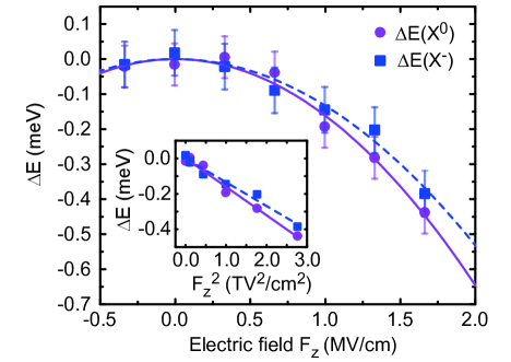
Although the polarizabilities were measured at an electron density of , and should remain constant for carrier densities lower than where the conventional excitonic picture is valid Sidler et al. (2016); Efimkin and MacDonald (2017). The transition to a many-body description occurs at higher electron densities than those used here. The slightly smaller polarizability of X- with respect to X0 can be explained by Coulomb effects. Specifically, in the X- complex there is an additional decrease in the exciton binding energy with electric field. This is induced by the localization of the two electrons on one side of the monolayer, increasing the electron-electron repulsion Shields et al. (1998). The excitonic polarizabilities have been theoretically calculated with a finite barrier quantum well model Pedersen (2016). Using barriers of 2.8 eV Choi et al. (2013) for both electron and hole, a quantum well thickness of 0.65 nm and effective electron and hole masses of 0.35 bare electron mass Mak et al. (2013), an exciton polarizability of is deduced which is in good agreement with the values reported here.
In conclusion, the QCSE of excitons has been extracted from photoluminescence measurements on a high quality MoS2 monolayer embedded in a vdWh. As the electron density in the monolayer is observed to vary with electric field, a careful data analysis exploiting reference measurements on a directly contacted MoS2 device was performed. Regions were identified in which the carrier density in the monolayer remains constant as the electric field is varied. Having ruled out any contribution of a changing electron density to the exciton energy shift, a QCSE was unambiguously identified. The small exciton polarizability is in line with theoretical computation Pedersen (2016). The maximum QCSE achieved here corresponds to just half the homogeneous linewidth despite the fact that large eletric fields were applied. The insensitivity of the exciton to an electric field in MoS2 has profound implications on its optical properties. On the one hand, we believe that the minute QCSE renders the exciton energy insensitive to charge noise. This, along with the super-fast radiative decay, explains the observation of optical linewidths close to the homogeneous limit in MoS2 vdWhs Cadiz et al. (2017). On the other hand, electrical control of the exciton based on the QCSE would require larger polarizabilities or a non-zero dipole moment as observed in heterobilayers for instance Rivera et al. (2015). The methodology used here to determine the QCSE in MoS2 can be used also in other semiconducting monolayers, where similar values of the polarizability should be obtained owing to the extreme out-of-plane confinement of both electrons and holes.
Acknowledgements.
We thank M. Munsch for fruitful discussions. We acknowledge financial support from SNF Project 200020_175748, Swiss Nanoscience Institute, QCQT PhD School, NCCR QSIT and Graphene Flagship. Growth of hexagonal boron nitride crystals was supported by the Elemental Strategy Initiative conducted by the MEXT, Japan and JSPS KAKENHI Grant Numbers JP15K21722.I Methods
Device fabrication
Van der Waals heterostructures were fabricated by stacking two-dimensional materials via a dry-transfer technique Zomer et al. (2014). All layers were mechanically exfoliated from bulk crystals (natural MoS2 crystal from SPI Supplies, synthetic h-BN Taniguchi and Watanabe (2007) and natural graphite from NGS Naturgraphit). MoS2 monolayers were treated by a bis(tri-fluoromethane)sulfonimide (TFSI) solution following Ref. Amani et al., 2015 before full encapsulation between h-BN layers. Few-layer graphene was employed as a top transparent electrode or as a contact electrode to MoS2 Yu et al. (2014). Metal contacts to FLG were patterned by electron-beam lithography and subsequent metal deposition of Au (45 nm)/Cr (5 nm). The flake thickness of each layer was characterized by a combination of optical contrast, atomic force microscopy, PL and Raman spectroscopy. The data shown in this Letter were measured on a device consisting of SiO2 (300 nm)/h-BN (5.4 nm)/MoS2 (0.65 nm)/h-BN (12 nm)/FLG (17 nm).
Photoluminescence measurements
Photoluminescence spectroscopy was performed in a liquid He bath cryostat using a home-built confocal microscope setup. The main sample and the reference sample were optically excited using a linearly polarized diode laser at photon energy 2.32 eV (wavelength 535 nm) and a HeNe laser at photon energy 2.09 eV (wavelength 594 nm) with an intensity below , respectively. The collected light was dispersed onto a charged-coupled device array by a single monochromator equipped with a 1500 grooves/mm grating.
References
- Mak et al. (2010) K. F. Mak, C. Lee, J. Hone, J. Shan, and T. F. Heinz, “Atomically Thin : A New Direct-Gap Semiconductor,” Phys. Rev. Lett. 105, 136805 (2010).
- Splendiani et al. (2010) A. Splendiani, L. Sun, Y. Zhang, T. Li, J. Kim, C.-Y. Chim, G. Galli, and F. Wang, “Emerging Photoluminescence in Monolayer ,” Nano Lett. 10, 1271–1275 (2010).
- Geim and Grigorieva (2013) A. K. Geim and I. V. Grigorieva, “Van der Waals heterostructures,” Nature 499, 419–425 (2013).
- Novoselov et al. (2016) K. Novoselov, A. Mishchenko, A. Carvalho, and A. Castro Neto, “2D materials and van der Waals heterostructures,” Science 353, aac9439 (2016).
- Chernikov et al. (2014) A. Chernikov, T. C. Berkelbach, H. M. Hill, A. Rigosi, Y. Li, O. B. Aslan, D. R. Reichman, M. S. Hybertsen, and T. F. Heinz, “Exciton Binding Energy and Nonhydrogenic Rydberg Series in Monolayer ,” Phys. Rev. Lett. 113, 076802 (2014).
- Miller et al. (1984) D. A. B. Miller, D. S. Chemla, T. C. Damen, A. C. Gossard, W. Wiegmann, T. H. Wood, and C. A. Burrus, “Band-edge electroabsorption in quantum well structures: The quantum-confined Stark effect,” Phys. Rev. Lett. 53, 2173–2176 (1984).
- High et al. (2008) A. A. High, E. E. Novitskaya, L. V. Butov, M. Hanson, and A. C. Gossard, “Control of exciton fluxes in an excitonic integrated circuit,” Science 321, 229–231 (2008).
- Schinner et al. (2013) G. J. Schinner, J. Repp, E. Schubert, A. K. Rai, D. Reuter, A. D. Wieck, A. O. Govorov, A. W. Holleitner, and J. P. Kotthaus, “Confinement and interaction of single indirect excitons in a voltage-controlled trap formed inside double InGaAs quantum wells,” Phys. Rev. Lett. 110, 127403 (2013).
- Schuller et al. (2013) J. A. Schuller, S. Karaveli, T. Schiros, K. He, S. Yang, I. Kymissis, J. Shan, and R. Zia, “Orientation of luminescent excitons in layered nanomaterials,” Nat. Nanotechnol. 8, 271–276 (2013).
- Klein et al. (2016) J. Klein, J. Wierzbowski, A. Regler, J. Becker, F. Heimbach, K. Müller, M. Kaniber, and J. J. Finley, “Stark effect spectroscopy of mono- and few-layer MoS2,” Nano Lett. 16, 1554–1559 (2016).
- Guo et al. (2015) Y. Guo, X. Wei, J. Shu, B. Liu, J. Yin, C. Guan, Y. Han, S. Gao, and Q. Chen, “Charge trapping at the MoS2-SiO2 interface and its effects on the characteristics of MoS2 metal-oxide-semiconductor field effect transistors,” Appl. Phys. Lett. 106, 103109 (2015).
- Pedersen (2016) T. G. Pedersen, “Exciton Stark shift and electroabsorption in monolayer transition-metal dichalcogenides,” Phys. Rev. B 94, 125424 (2016).
- Chernikov et al. (2015) A. Chernikov, A. M. van der Zande, H. M. Hill, A. F. Rigosi, A. Velauthapillai, J. Hone, and T. F. Heinz, “Electrical tuning of exciton binding energies in monolayer WS2,” Phys. Rev. Lett. 115, 126802 (2015).
- Sidler et al. (2016) M. Sidler, P. Back, O. Cotlet, A. Srivastava, T. Fink, M. Kroner, E. Demler, and A. Imamoğlu, “Fermi polaron-polaritons in charge-tunable atomically thin semiconductors,” Nat. Phys. 13, 255 (2016).
- Efimkin and MacDonald (2017) D. K. Efimkin and A. H. MacDonald, “Many-body theory of trion absorption features in two-dimensional semiconductors,” Phys. Rev. B 95, 035417 (2017).
- Cadiz et al. (2017) F. Cadiz, E. Courtade, C. Robert, G. Wang, Y. Shen, H. Cai, T. Taniguchi, K. Watanabe, H. Carrere, D. Lagarde, M. Manca, T. Amand, P. Renucci, S. Tongay, X. Marie, and B. Urbaszek, “Excitonic linewidth approaching the homogeneous limit in MoS2-based van der Waals heterostructures,” Phys. Rev. X 7, 021026 (2017).
- Mak et al. (2013) K. F. Mak, K. He, C. Lee, G. H. Lee, J. Hone, T. F. Heinz, and J. Shan, “Tightly bound trions in monolayer MoS2,” Nat. Mater. 12, 207–211 (2013).
- Manassen et al. (1996) A. Manassen, E. Cohen, A. Ron, E. Linder, and L. N. Pfeiffer, “Exciton and trion spectral line shape in the presence of an electron gas in GaAs/AlAs quantum wells,” Phys. Rev. B 54, 10609–10613 (1996).
- Hawrylak (1991) P. Hawrylak, “Optical properties of a two-dimensional electron gas: Evolution of spectra from excitons to Fermi-edge singularities,” Phys. Rev. B 44, 3821–3828 (1991).
- Ju et al. (2014) L. Ju, J. Velasco Jr, E. Huang, S. Kahn, C. Nosiglia, H.-Z. Tsai, W. Yang, T. Taniguchi, K. Watanabe, Y. Zhang, et al., “Photoinduced doping in heterostructures of graphene and boron nitride,” Nat. Nanotechnol. 9, 348–352 (2014).
- Epping et al. (2016) A. Epping, L. Banszerus, J. Güttinger, L. Krückeberg, K. Watanabe, T. Taniguchi, F. Hassler, B. Beschoten, and C. Stampfer, “Quantum transport through MoS2 constrictions defined by photodoping,” arXiv preprint arXiv:1612.01118 (2016).
- Choi et al. (2013) M. S. Choi, G.-H. Lee, Y.-J. Yu, D.-Y. Lee, S. H. Lee, P. Kim, J. Hone, and W. J. Yoo, “Controlled charge trapping by molybdenum disulphide and graphene in ultrathin heterostructured memory devices,” Nat. Commun. 4, 1624 (2013).
- Wang et al. (2010) H. Wang, Y. Wu, C. Cong, J. Shang, and T. Yu, “Hysteresis of electronic transport in graphene transistors,” ACS Nano 4, 7221–7228 (2010).
- Shields et al. (1998) A. Shields, J. Osborne, M. Simmons, D. Whittaker, F. Bolton, D. Ritchie, and M. Pepper, “Stark effect of negatively and positively charged excitons in semiconductor quantum wells,” Physica E 2, 87–92 (1998).
- Rivera et al. (2015) P. Rivera, J. R. Schaibley, A. M. Jones, J. S. Ross, S. Wu, G. Aivazian, P. Klement, K. Seyler, G. Clark, N. J. Ghimire, et al., “Observation of long-lived interlayer excitons in monolayer MoSe2–WSe2 heterostructures,” Nat. Commun. 6 (2015).
- Zomer et al. (2014) P. Zomer, M. Guimarães, J. Brant, N. Tombros, and B. Van Wees, “Fast pick up technique for high quality heterostructures of bilayer graphene and hexagonal boron nitride,” Appl. Phys. Lett. 105, 013101 (2014).
- Taniguchi and Watanabe (2007) T. Taniguchi and K. Watanabe, “Synthesis of high-purity boron nitride single crystals under high pressure by using Ba–BN solvent,” J. Cryst. Growth 303, 525–529 (2007).
- Amani et al. (2015) M. Amani, D.-H. Lien, D. Kiriya, J. Xiao, A. Azcatl, J. Noh, S. R. Madhvapathy, R. Addou, K. Santosh, M. Dubey, et al., “Near-unity photoluminescence quantum yield in MoS2,” Science 350, 1065–1068 (2015).
- Yu et al. (2014) L. Yu, Y.-H. Lee, X. Ling, E. J. G. Santos, Y. C. Shin, Y. Lin, M. Dubey, E. Kaxiras, J. Kong, H. Wang, and T. Palacios, “Graphene/MoS2 hybrid technology for large-scale two-dimensional electronics,” Nano Lett. 14, 3055–3063 (2014).