Evolution and Recent Developments of the Gaseous Photon Detectors Technologies
Abstract
The evolution and the present status of the gaseous photon detectors technologies are reviewed. The most recent developments in several branches of the field are described, in particular the installation and commissioning of the first large area MPGD-based detectors of single photons on COMPASS RICH-1. Investigation of novel detector architectures, different materials and various applications are reported, and the quest for visible light gaseous photon detectors is discussed. The progress on the use of gaseous photon detector related techniques in the field of cryogenic applications and gaseous or liquid scintillation imaging are presented.
keywords:
Photon detectors , gaseous detectors , MPGD , THGEM , CsI , photocathodes1 Introduction
The development of gaseous detectors started more than 100 years ago and provided the fundamental physics research community with great inventions: the Wire Counter, the Cloud Chamber, the Geiger-Mueller Counter, the Spark Chamber, the Bubble Chamber, the Parallel Plate Avalanche Chamber, the Multi-Wire Proportional Chamber (MWPC), the Drift Chamber, the Time Projection Chamber (TPC), the Limited Streamer Tubes, the Resistive Plate Chamber and many other detectors allowed to perform critical and previously impossible measurements. In the last 30 years various technologies, collectively named Micro-Pattern Gaseous Detectors (MPGDs) have been introduced to overcome the particle flux capability limitations of MWPCs and achieve higher space resolution, starting from the Micro-Strip Gas Counter (MSGC) [1], followed by the successful and wide-spread MicroMegas (MM) [2] and Gas Electron Multiplier (GEM) [3] detectors.
The use of old gaseous detector technologies is declining but an impressive development of new techniques, based both on the consolidation and spread of recent ideas and on the appearance of new elements is opening fascinating perspectives for the years to come.
A similar evolution took place in the domain of photon detection leading to the introduction of many successful devices and techniques; nowadays both vacuum based Photon Detectors (PDs), in particular Multi-Anode PhotoMultiplier Tubes and Micro-Channel Plates and solid state based PDs, in particular Si-PMTs and Avalanche Photo-Diodes are commercially available technologies and provide excellent and greatly improving performance; their use is increasing and their application range is spreading.
Gaseous PDs instead are not commercially available, but they offer specific and unique characteristics: a cost-effective solution to cover very large areas with photosensitive detectors, very low material budget and minimal sensitivity to magnetic fields.
Gaseous PDs have played an essential role in establishing Ring Imaging CHerenkov Counters (RICHs) technology and the continuous development of gaseous PDs has recently been accelerated.
This article aims to illustrate this acceleration, after mentioning some of the main characteristics and achievements in the field of gaseous PDs, and to describe some of the present activities which can potentially lead to important future advancements.
2 MWPC-based PDs
The need from High Energy Physics Experiments of performing hadron identification in a wide range of momenta and over a wide angular acceptance motivated the quest for equipping large area of efficient detectors of single Cherenkov photons at affordable cost. In 1980 suitable photo-ionizing agents: Tri-Ethyl-Amine (TEA) [4] and Tetrakis Dimethylamine Ethylene (TMAE) [5] became available and could be coupled with large area position sensitive gaseous detectors (MWPCs). Two conflicting requirements however had to be composed: a high efficiency in conversion and detection of Cherenkov UV photons, implying a multiplication gain large enough to allow detecting single photoelectrons and a limited sensitivity to the UV photons copiously emitted in the large avalanche process without using a photon quencher which would kill the primary signal.
The first solution was the Multi-step Avalanche Chamber, developed by Charpak and Sauli [6] and used by the RICH of E605 Experiment [7] [8] at FNAL with TEA vapour and CaF2 windows. MWPC-based PDs with TEA and CaF2 windows were also used by CLEO III [9]. Using TEA in a CH4 atmosphere, the detected photon wavelength range is limited to the far UV interval between 135 and 165 nm, where very few materials are transparent and the chromatic dispersion is large: E605 indeed used He, the lowest chromaticity gas, as radiator.
TMAE has a low photo-ionization threshold (5.3 eV) and is compatible with the use of fused silica windows: the resulting effective wavelength range for photon detection is between 160 nm and 220 nm. The largest RICH detectors ever built: the DELPHI RICHs [10], the SLD CRID [11] and the OMEGA RICH [12] [13] used TMAE and a PD based on the TPC RICH concept [14]. Due to the low TMAE vapor pressure at room temperature the photon conversion gap needs to be centimeters thick and the detectors were operated at high temperature (40 degrees or even 50 degrees in the case of CERES RICH [15]). The photoelectrons were drifted in a uniform electric field toward MWPCs to obtain a 3D imaging, which was needed to correct for the parallax error affecting the photon conversion in a thick gap. The long drift time made these detectors intrinsically slow and spurious signals were generated by the conversion of photons produced in the amplification process; against them special blinds had been inserted between wires in the RICH MWPCs [16]. The extreme chemical reactivity of TMAE severely restricts the choice of detector materials and the tolerance of gas impurities [17].
TMAE emits visible light: TMAE-based optical readout of RICH detectors [18] was implemented in the NA35 Experiment [19].
The photo-converting property of a thin film of CsI for UV photons is known since 1956 [20], and vacuum operated photocathodes had been developed for space astronomy [21]. The first position sensitive gas detectors with CsI photocathodes were developed at the end of the 80s [22] [23].
Semi-transparent CsI photocathodes are commonly used in vacuum-based PDs, and they could as well be used for gaseous-based PDs. Their photon conversion efficiency is limited by the need to deposit a thin conductive layer on the window which absorbs a non-negligible fraction of UV photons and by the need to optimize the thickness of the CsI layer [24]: a thinner layer has lower photon absorption probability, a thicker one has a lower escape probability for the photoelectron. The strict requirement on CsI thickness uniformity makes the production of large area semitransparent CsI photocathodes technically difficult. The reflective option has indeed been chosen for all CsI gaseous-based PD photocathodes used in large experiments.
Due to its sensitivity to the substrate and its degradation in the presence of humidity many years were needed to develop an optimized procedure for production and handling of large area CsI photocathodes for gaseous PDs. This technology was pioneered by T. Ypsilantis ad J. Séguinot [25] and developed by the RD26 Collaboration [26] coordinated by F. Piuz. The technology of large area gaseous PDs with solid photo-converter for RICH applications represented a real breakthrough; it is based on the use of MWPCs with thin gap (2 mm), cathode wires of 100 m diameter and 2 mm pitch, anode wires of 20 m diameter and 4 mm pitch and CsI photocathodes segmented in 8 8 mm2 pads. [27]. The PDs are operated in pure CH4 to minimize the photoelectron backscattering [28].
An optimized photocathode production procedure [29] [30] for achieving high QE was defined, involving proper substrate preparation (Cu-clad PCB coated with 7 m Ni and 0.5 m Au), ultrasonic bath cleaning and out-gassing, a slow deposition (1 nm/s) of a 300 nm thick CsI layer by thermal evaporation (at about 10-7 mbar) followed by a thermal treatment (8 h at 60 ∘C). Essential parts of the procedure are: the mapping of the local photocathode response, the encapsulation and flushing with dry gas during storage and the handling under controlled atmosphere using glove-boxes.
RD26-type MWPC-based PDs have been [31] and still are successfully used by several experiments: NA44 [32] at CERN, HADES [33] at GSI, COMPASS [34] at CERN (5.5 m2 active area), STAR [35] at RHIC, HALL-A [36] at JLAB, ALICE [37] at CERN (10 m2 active area), etc. The impact of MWPC-based PDs on the physics results of the experiments is very relevant and they can be considered the classical successful gaseous PDs. Their use had been proposed for the upgrade of ALICE HMPID [38].
The aging of CsI has been investigated in detail [39] and is reported to result in a severe decrease of the quantum efficiency after a total collected charge of few mC/cm2. Aging is mainly caused by the Ion Back-Flow (IBF) to the photocathode, namely the bombardment of the CsI layer by the positive ions generated in the multiplication process.
The CsI photocathodes used in gaseous PDs preserve their QE over a period of many years with at most a modest decrease [40] [41] [42].
MWPC-based PDs have intrinsic limits on rate capability and time resolution; they have to operate at relatively low gain, because of their open geometry: secondary effects from photon feedback and large ionization events can otherwise generate electrical instabilities [43]. Their readout signals derive from the slow motion of ions and they have long detector memory, even when coupled to upgraded front-end electronics [44]. The aging is accelerated by their large IBF. To achieve the higher performance needed in high rate applications, a technology change was needed [45].
3 GEM-based PDs
The progress of photo-lithography and other technologies in mastering the production of complex patterns with accuracy at the 10 m level or better allowed the development of many MPGDs (MSGCs [1], Micro-Gap [46], Micro-Dot [47], Compteur à Trous [48], MM [2], GEM [3], Micro-Groove [49], Micro-Wire Chamber [50], Micro-Pin Array [51] Micro-Pixel [52], Field Gradient Lattice [53], etc.). Among them MM and GEM are fully mature and consolidated technologies, ubiquitously used for the detection of particles.
MMs are parallel plate chambers built with a thin metal grid stretched and kept at a small, uniform distance (about 100 m) from the readout electrode by isolating supports; operated with electric field above 30 kV/cm they provide proportional multiplication of the electric charge entering the high field region from the open spaces of the grid. MMs are robust and have low sensitivity to small gap variation or imperfections. They provide good energy resolution and, thanks to the large difference in the electric field in the regions above and below the grid, a dominant fraction of the ions produced in the multiplication is collected by the grid [54].
GEM consist of 50 m thin, copper-clad polyimide foils with a high density regular matrix of holes, produced by photo-lithography and chemical etching processes. Inserted between a drift and a collection electrode and properly biased, they provide proportional multiplication of the ionization electrons produced in the drift region and efficient transfer of electrons into the collection region. The multiplication occurs mainly inside the holes of the GEM, the chamber readout electrode is physically independent from the GEM and the signal is fast, being generated only by electrons. Several GEM layers can be cascaded in the same detector [55], allowing discharge free operation, good space and time resolution [56] [57] and high rate capability [58].
Detectors based on a triple-GEM amplification have been pioneered by the COMPASS experiment at CERN [59], and are routinely used in particle physics experiments (LHCb [60], PHENIX [61], KLOE-2 [62] TOTEM [63]) and proposed for the upgrade of CMS [64] [65] [66].
The MPGD developers community is actively improving the MM, GEM and other technologies; it has a reference, world-wide forum of discussion, where common standards are defined and access to common facilities is granted, in the RD51 Collaboration [67] at CERN. Innovative proposals and freshly obtained test results are frequently compared and new ideas continuously appear and compete in this forum.
The use of a GEM as a first amplifier in a gaseous PD [68] was proposed as soon as the GEM was invented, to exploit its low optical transparency. After a first prototype with a semi-transparent photocathode [69], a multi-layer GEM structure having a CsI coating on the top of the first GEM [70] was developed and successfully operated by PHENIX-HBD [71]. This detector represents the first application of MPGD-based photon counters in an experiment. The PDs [72] are triple GEMs covering about 1.5 m2. The detector is windowless and operates with a gain of about 5000 in pure CF4. The CsI layer on the first GEM converts the Cherenkov photons produced in the 50 cm thick radiator gas volume, over a wide wavelength range (108-200 nm). The large (6.2 cm2) readout pads provide collective signals from several (5 to 10) Cherenkov photons. The identification of low-mass di-leptons requires efficient hadron blindness which is achieved by using CF4 as radiator medium (so that hadrons in the momentum range studied by PHENIX do not emit Cherenkov photons) and a slightly reversed field in the radiator region which repels the ionization electrons released by charged particle tracks.
GEM-based PDs provide fast signals (time resolution 2 ns) [70] and do suppress the photon feedback thanks to their closed geometry, but in order to efficiently detect single photons they should operate at higher gain than in the PHENIX-HBD case and to be suitable for high rate operation they should limit the IBF to the photocathode, to preserve it from aging and avoid secondary effects causing electrical instability.
IBF in multi-GEM structures with semi-transparent [73] or reflective [74] photocathodes can be reduced to 2% and 10% respectively without affecting the total gain; less than 1% IBF is obtained with very low values of the drift field [75]; this option however is not suited for a PD with reflective photocathode because the CsI photoelectron extraction efficiency at low electric field values at the CsI surface is too low.
More elaborate GEM structures have been introduced to achieve higher IBF suppression. The Micro Hole and Strip Plate (MHSP) [76] has one of the two GEM surfaces segmented and equipped with microstrips allowing for further amplification or for ion trapping [77]: an IBF of 310-4 at a gain of 105 in Ar/CH4 95/5 has been obtained using multiple MHSPs in reverse bias mode [78]. Extremely low values of the IBF ( 10 have been achieved using specially shaped MHSP called COBRA [79]. The possibility to collect a large fraction of the ions in the intermediate electrodes is of particular interest for visible light gaseous PDs and for TPC applications [80] [81]; for the latter case all GEM electrodes can be used for IBF suppression. An optimization of GEM detectors for the ALICE-TPC upgrade [82] achieved less than 1% IBF in a quadruple GEM structure with largely unbalanced transfer field values and different hole patterns in different GEM layers [83]. GEM-based PDs have been proposed for cryogenic applications too.
The typical gain of multi-GEM detectors used as trackers in experiments is mostly below or around 104, despite the fact that they achieve 105 or more in laboratory tests.
A high-gain alternative electron multiplier has been introduced for the detection of single photons.
4 THGEM-based PDs and the Hybrid PD’s of COMPASS RICH-1
Thick-GEMs (THGEMs) are gaseous electron multipliers derived from the GEM design, scaling the geometrical parameters and changing the production technology: standard Printed Circuit Boards (PCBs) are used instead of the copper-clad polyimide foils and the holes are obtained by drilling. They were introduced in parallel by several groups [84] [85] [86] [87] [88].
THGEMs are simple, mechanically stiff, electrically robust and cost effective; they have typical thickness of 0.2-1.2 mm, cylindrical holes with diameter in the 0.2-1.0 mm range and pitch of 0.4-2.0 mm. Their holes can be provided with a rim, a clearance ring in the Cu layers around the holes which can vary from 0.0 to 0.2 mm in width. They can be industrially manufactured in large series and large size using standard PCB drilling and etching techniques.
In comparison with the GEM case, the space resolution provided by THGEM-based detectors is modest [89] (1 mm) and the material budget is large, but the electron collection and transport is more effective [90] (for THGEMs the electron transverse diffusion is smaller than the hole diameter) and the achievable gains are larger [91] [92].
THGEMs with different geometrical parameters have been extensively characterized and their role as electron multipliers and as reflective photocathode has been studied in detail [93] [94] [95] [96] [97]. A special role is played by the rim: the maximum achievable gain increases exponentially with the rim size [93] but large gain variations over time and significant gain dependence on the irradiation history [98] [99] are seen for large rim THGEMs.
Apart from standard THGEMs, produced from PCB material (FR4), special THGEMs have been produced using different substrate materials, including noble substrates (ceramic [100], glass [101] [102] [103]), organic substrates (Kevlar, PTFE [104], etc.) or using different production procedures, including water jet or laser drilling and chemical etching. The technology for Capillary Plates (CP) production, typically used in vacuum-based PDs, provides multipliers for hole-type MPGDs which could be included in the THGEM category too.
THGEMs can be treated to have the holes covered by highly isolating films (polyurethane) or the electrodes covered by resistive layers: an intense investigation of this design, called RETGEM (PCBs covered with resistive kapton layers) has been performed [105].
Interesting THGEMs with different structures have been produced, in particular the analogue of the GEM COBRA: the THCOBRA [106], discussed in Section 5, the Multi-layer THGEM [107] and the Blind-THGEM, also called WELL [108] (from the name of a MPGD proposed in 1999 by Bellazzini [109]) namely a THGEM with a closed bottom anode, also in the resistive-anode version, discussed in Section 5 too.
Chambers hosting multilayer standard THGEMs arrangements with CsI coating on the top of the first THGEM [93] have been built and operated in Ar-based and in Ne-based gas mixtures [110] [111].
High gain, stable operation in laboratory and at test beam lines [112] have been reported for small-size prototypes of various configurations, in particular with triple identical THGEMs, the first one being CsI-coated: effective gain in the range of 105-106 [113] are commonly achieved, and time resolutions below 10 ns [114] are typical.
Obtaining the same performance in terms of gain and stability with large or medium size (300 300 cm2) triple THGEM PDs was more challenging: a dedicated R&D program [95] [115] investigating the origin of non-uniformity of the detector response and the spark rates as well as the performance of different PD configurations provided a specific procedure for large area THGEM production [116], quality assessment and configuration optimization. An investigation of the IBF [117], which in a standard triple THGEM configuration approaches 30%, showed that it can be reduced by a complete misalignment of the holes in different layers and using unbalanced values of the electric field in the transfer regions between THGEMs (as in the GEM case [80]).
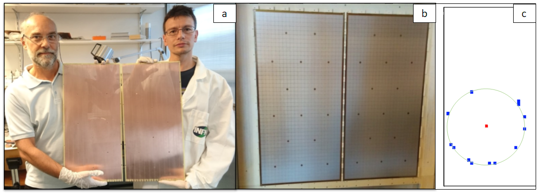
To achieve a further IBF suppression an alternative architecture combining MM and THGEM technologies was tested and provided better results in terms of PD performance and stability for large area prototypes [118]. This hybrid configuration has been chosen for the COMPASS RICH-1 upgrade [119], performed in 2016: four new MPGD-based PDs [120], covering a total active area of 1.4 have been installed replacing MWPC-based PDs which were in operation since 2002; for the first time MPGD-based detectors of single photons were used in a running experiment [121].
The new detector architecture consists in a hybrid MPGD combination (see Fig.1) of two THGEMs, the first acting as reflective photocathode, and a Micromegas on a pad segmented anode.
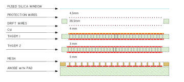
Each of the four PDs covers a 600 600 mm2 active area and is formed by two identical modules (600 300 mm2), arranged side by side. Two planes of wires are located respectively at 4 mm from the CsI coated THGEM and at 4.5 mm from the fused silica window of the PD. They allow the tuning of the electric field in the region above the photocathode in order to optimize the photoelectron collection and repel the ionization electrons. All THGEMs (Fig. 2, a) have the same geometrical parameters: they are 470 m thick (400 m dielectric and 2 35 m Cu), their holes have 400 m diameter, 800 m pitch and no rim. Holes located along the external borders have 500 m diameter. The electrodes are segmented in 24 mm wide strips and the voltage bias is individually provided to each sector of the THGEMs through protection resistors; accurate raw material selection, post-production treatments and validation tests were performed.
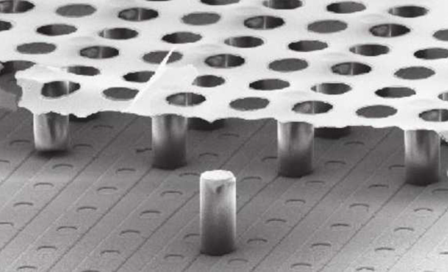
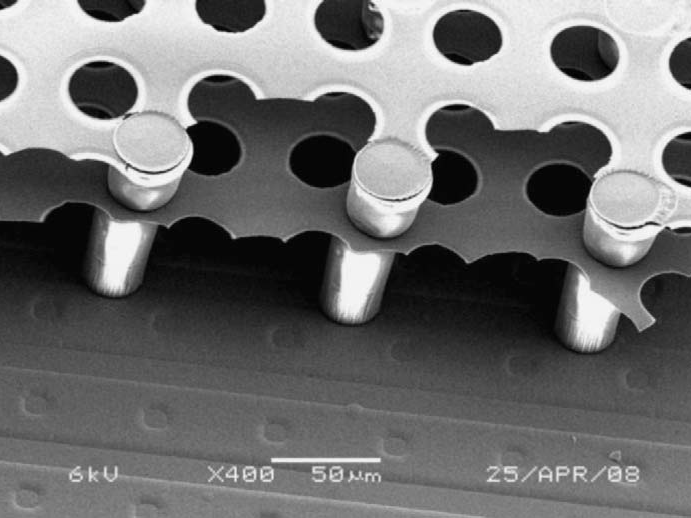
The two THGEM layers are mounted at a distance of 3 mm, in a configuration of complete hole misalignment, to achieve the maximum charge spread; 5 mm separate the middle THGEM from the MMs. The MMs (Fig. 2, b) were produced at CERN using the bulk technology procedure [122] [123]: they have a 128 m gap, 18 m woven stainless steel wire mesh with 63 m pitch; a square array of 300 m diameter pillars with 2 mm pitch keeps the micromesh in place, on a PCB specifically designed for COMPASS RICH-1. The square anode pads facing the micromesh have 8 mm pitch and 0.5 mm inter-pad clearance and are biased at positive voltage; the micromesh, which is the only non-segmented electrode, is kept at ground potential. Each anode pad receives the biasing voltage via an individual 470 M resistor.
The signal is transmitted from the anode pad via capacitive coupling to a readout pad facing it, buried inside the anode PCB (at 70 m distance from the anode pad) and connected by a short path to the front-end board connector. The resistive-capacitive pad scheme dumps the effects of discharges and protects the front-end electronics [44], which is based on the APV25 chip.
COMPASS hybrid PDs operate with an Ar/CH4 50/50 gas mixture, at transfer field values of 1.5 kV/cm between THGEMs and 0.8 kV/cm between the MM and the THGEMs. The typical effective gain values are few 104 and the noise level is 900 equivalent electrons r.m.s. [120]. The IBF to the photocathode is 3%. A high voltage monitoring program stabilizes the gain by tuning the biases applied to MM and THGEMs to compensate for the environmental changes of temperature and pressure.
The COMPASS hybrid PDs have been commissioned in 2016 and provided stable performance during the 2017 run: an example of their Cherenkov rings is presented in Fig. 2, c. The validity of the MPGD-based PD approach for RICH applications is confirmed by the successful operation of COMPASS hybrid PDs.
5 Other gaseous PDs sensitive in the UV domain
Some gaseous PDs could provide unique characteristics for special applications: very high space resolution, extremely reduced material budget, precise timing etc. Few examples are mentioned in this section.
Following the idea of active pixel readout of GEMs [124] a UV-sensitive gaseous detector [125], based on a CsI semi-transparent photocathode, a GEM charge multiplier and a self-triggering CMOS analog pixel chip with 105 k pixels at 50 m pitch was built and shown to achieve an accuracy of 4 m rms in the coordinates of each GEM avalanche.
A similar hybrid architecture able to provide excellent space resolution for single UV photon detection is based on the use of InGrid technology [126] consisting of a MM (Al micro-grid) directly integrated by wafer post-processing production onto a CMOS pixel detector with the complete readout system (see Fig.3).
The micro-grid is sustained on pillars located at the intersection of four adjacent pixels while the array of micro-grid round holes corresponds to the array of CMOS pixel centers (square pattern with 55 m pitch). CsI coating of the micro-grid, which has an optical transparency of 20%, provides photo-sensitivity. Using a He/i-C4H10 80/20 gas mixture a gain of 6104 has been obtained. Several other detectors with similar architectures (produced by wafer post-processing) have been tested, including a TwinGrid [127] with a double metal grid onto the CMOS pixel chip. The use of a 10 m thick protection layer of hydrogenated amorphous silicon or silicon-rich nitride with high resistivity is shown [128] to quench the sparks and limit the maximum charge provided by discharge signals. Detectors based on the combination of InGrids with the Timepix ASIC [129], called GridPix [130] have also been used as TPC readout elements and for X-Ray detection (in the CAST experiment at CERN).
An option to minimize the material budget of a PD is the use of GEMs with Al clad or thinner Cu clad or even with the Cu etched away (leaving only the 100 nm thik Cr layer normally used as a tie coat for the adhesion of Cu): a reduction down to 10-3 X0 [131] [132] could be reached.
Windowless GEMs with CsI are proposed for particle identification at a future Electron Ion Collider [133] facility for a focusing RICH and a for a combined TPC/Cherenkov detector, both operating with pure CF4 or CF4-rich gas mixtures. For the focusing RICH a prototype with 1 m long CF4 radiator, a mirror with high reflectivity at 120 nm and windowless quintuple-GEMs + CsI, has recently been tested [134]. It is proposed to operate the central tracking TPC with CF4 and equip it with gaseous PDs located inside the TPC gas volume, performing UV photon conversion and electron multiplication in the same gas; these PDs could be similar to PHENIX HBD GEM-based ones and could use Cherenkov light signals to identify electrons with the PHENIX HBD technique. The compatibility of these PDs with the delicate TPC operation is being actively investigated [135].
The THCOBRA [106] is a THGEM having one of the faces equipped with additional anode strips winding between circular cathode strips. Primary avalanches occurring within the holes are followed by additional ones at the anode-strips vicinity.
The THCOBRA has been used coupled with THGEMs for IBF suppression [136]. An evolution of the THCOBRA concept, namely a THCOBRA having the other face segmented in strips orthogonal to the COBRA strips (see Fig. 5) has been used as both electron multiplier and readout element, allowing for a position sensitive detector to be built without a separate anode readout systems. A small PD consisting of a THGEM with CsI, a second THGEM and the strip THCOBRA (see Fig. 4 and 5) has been built and demonstrated to provide good VUV sensitivity and space resolution with very simple electronics readout.
The Resistive-Plate WELL (RPWELL) [137] is a novel gaseous multiplier based on the WELL concept. It is made of a single-sided copper-clad THGEM electrode, coupled to a segmented readout anode (pads or strips) through a thin high bulk-resistivity plate. It demonstrated discharge-free operation at high gas-avalanche gains and over a broad ionization range [138] [139]. It has recently been proposed to exploit the high stability of the RPWELL multiplier to develop a gaseous PD similar to the COMPASS RICH Hybrid one, with Micromegas replaced by RPWELLs (see Fig. 6), making use of silicate glass resistive plates with 109 cm [140].
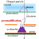
The quest for a detector able to provide very high time resolution in a high rate environment triggered the investigation of a Cherenkov light detector with minimal time jitter [141]. A Micromegas PD has been constructed in order to study the potential for 20 ps timing for charged particles [142]. It consists of a small amplification gap (64 m), a thin mesh (10 nm Al) coated with CsI to act as a reflective photocathode or, in the semitrasparent version, a CsI photocathode window separated by a small gap with voltage bias large enough to provide preamplification: in the latter condition (Fig. 7, left), a single photon time resolution of 200 ps has been measured, providing encouraging indications for the possibility to achieve the desired time resolution goal.
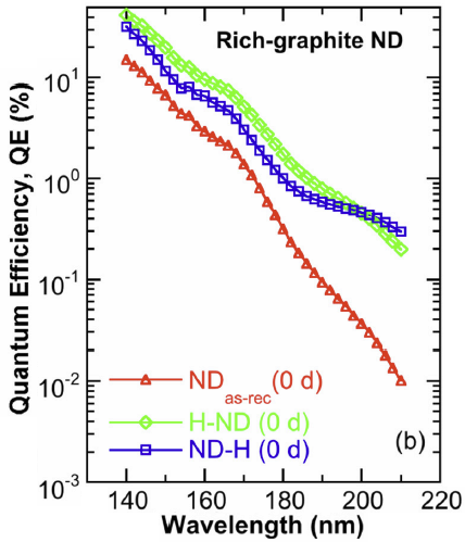
(left) and measured QE of hydrogenated rich-graphite nanodiamond grains (right).
An important element for a future extensive use of Cherenkov photon conversion in harsh environments is a robust photocathode: intensive studies for alternatives to standard CsI are ongoing on either protective layers (graphene shield enhanced photocathodes [143] or different UV photocathode materials. A promising candidate has recently been identified: hydrogenated rich-graphite nano-diamond grains of 250 nm offer robustness and high QE [144] (see Fig. 7, right)
6 The quest for visible light gaseous PDs
The detection of Cherenkov light in the visible range brings several great advantages with respect to the far UV case: larger photon yield thanks to the larger bandwidth, better angular resolution thanks to the reduced chromaticity of the radiator, wider range of optical media with good transparency, including silica aerogel and larger tolerance to contaminants.
Combining these advantages with the opportunities offered by gaseous PDs (cost-effectiveness for large area, low material budget, magnetic insensibilty) is extremely appealing and a large R&D effort is being invested in developing the visible-light gaseous PD technology.
Due to the high chemical reactivity and the fragility of visible light photo-converters (alkali-antimony, bi- and multi-alkali), their use in gaseous detectors is a challenging task: most of the commonly used materials are incompatible with these photo-converters, ion-induced secondary electron emission is copious and aging by ion bombardment is quite fast. Coating photocathodes with protective films seriously reduces the QE [145].
Different detector architectures have been investigated for visible light gaseous PDs, from grid photomultipliers [146] to CP-based PDs [147]. A CP is a plate made of a bundle of fine glass capillaries fused together, uniformly arranged in a two-dimensional array. Typically, a CP thickness is ranging from 0.4 mm to 1 mm, and the capillary holes can be from 5 m to 50 m wide. A CP used as a hole-type MPGD [148] has metallic electrodes deposited on both surfaces. CPs have high temperature resistance and low out-gassing, making them suited for sealed devices, as in vacuum-based Micro Channel Plate (MCP)-PMT application. CPs have been used coupled to MM [149], also with the capillaries inclined [150] to achieve further reduction of the IBF. A recent development of funnel glass CP allows achieving 83% of surface area opening, and thus a higher photoelectron collection efficiency for semitransparent photocathode PDs. [151].
GEM-based gaseous PDs with bialkali photocathodes have been built and tested in sealed mode operation [152] [153], with an ion-blocking gate [154] or incorporating a Micro-Hole and Strip Plate (MHSP) into a Multi-GEM cascaded multiplier [155] or with flipped reverse-bias MHSP [156]: in the last case an IBF rate of 310-4 was achieved for a gain of 105. The polyimide GEMs material seems however to be incompatible with visible light photocathodes [157].
Good compatibility (no degradation after 2 y) is instead seen when using using MPGDs made of Pyrex glass plates and treated by sand micro-blasting, coupled with a Micromegas [158]. A dedicated system to study the gaseous PD QE degradation [159] allowed to measure for a semitransparent bialkali photocathode in a sealed gaseous PMT with micro-blasted glass CP and a 0.9 atm. of Ne/CF4 90/10 a QE reduction of about 20% after an integrated charge of 0.4 C/mm2.
Using two micromeshes with conical holes, produced by chemical etching, having holes of different diameter (120 m in the first and 80 m in the second micromesh) and common pitch of 250 m, arranged in a staggered pattern, with a bialkali photocathode and Ne/CF4 90/10 at 1 bar, a gain of 104 and an IBF of 610-4 have been obtained [160].
A recently explored alternative to overcome the IBF problem is the use of graphene, which is a single layer of carbon atoms arranged in a honeycomb lattice and is the thinnest material to date. A suspended graphene monolayer could be used as a micromesh with no transparency for gas molecules, atoms and ions, and possibly large transparency for electrons with kinetic energy of few eV [161]: if demonstrated to be effective and practically usable over large areas it could represent the ideal solution for the IBF suppression and open the way to the production of visible light gaseous PDs.
7 Cryogenic applications
Attempts to obtain high, stable electron multiplication directly in noble gases and liquids at cryogenic temperatures using open geometry gaseous multipliers (wires, needles or microstrips) have not been very successful [162] [163] until GEM-based detectors, called CRyogenic Avalanche Detectors (CRAD) [164] were introduced. With triple GEM detectors providing gains approaching 104 [165] the possibility to develop of a dual-phase CRAD equipped with CsI photocathode, able to detect both the charge ionization signal and the primary scintillation signals from liquid Ar (LAr) was demonstrated [166].
The use of THGEMs, (also called large Electron Multipliers: LEMs) was soon proposed [167] in view of giant LAr scintillation, Cherenkov and charge imaging experiment; THGEMs were indeed tested to be as effective as GEMs [168] for cryogenic applications [169] [170].
It has recently been shown [104] that THGEMs made of PTFE (Polytetrafluoroethylene) are particularly suited for cryogenic low noise applications because of their radiopurity.
A wide variety of gaseous PDs have been proposed and tested
[171]: they can be divided into three classes:
- PDs performing photon conversion and charge multiplication in a gas
separated by a window from the pure noble liquid (or gas) of the cryogenic detector.
- PDs operated directly in the noble gas of a dual-phase cryogenic detector.
- PDs immersed in the cryogenic noble liquid.
An example belonging to the first class is the Gaseous PhotoMultiplier (GPM) [172] formed by a triple THGEM (each having thickness = 0.4 mm, hole diameter = 0.4 mm, hole pitch = 0.8 mm, rim = 50 m) with active diameter of 100 mm, held 2 mm apart, with CsI on the first one, operated in Ne/CH4, coupled through a UV window to a small dual-phase LXe TPC. It has recently demonstrated the ability to record both single photon and massive electro-luminescence signals in the same operating conditions, with maximal gain above 105, assuring high single photon detection efficiency and stable operation.
A member of the second class is the dual-phase CRAD prototype [173] consisting of four THGEMs (10 10 cm2), two horizontally immersed in the LAr at 48 mm distance, biased to form a drift region in the liquid which covered the second THGEM by 4 mm, forming an electron emission region. A double-THGEM assembly with the first THGEM acting as the anode was placed 18 mm above the liquid surface, to form an electro-luminescence gap and provide multiplication. A matrix of Geiger Avalanche Photo-Diodes and cyogenic PMTs with wavelength shifters registered the scintillation light. A systematic study of the proportional electro-luminescence was performed. A recent measurement [174] showed that a small (50 ppm) N2 doping level of the Ar enhances the CRAD sensitivity to the proportional electro-luminescence signal.
A representative of the third class is the Liquid Hole Multiplier [175], proposed as a cascade of THGEMs (or analogous hole multipliers) with CsI photocathodes deposited on their surfaces, immersed in the noble liquid. Photoelectrons from primary scintillation or ionization electrons are focused into the electrode holes and give origin to electro-luminescence in the intense electric field in the liquid inside the holes; the amplification of the UV photons in the cascaded THGEM structure could result in detectable signals. Liquid Xe proportional electro-luminescence in THGEM holes was indeed observed [176] and its large intensity attributed to the possible presence of bubbles (local dual-phase conditions) near the THGEM holes [177], which have recently been directly observed [178]. The possibility to exploit this phenomenon in large-volume local dual-phase liquid TPCs is fascinating.
8 Scintillation imaging and other detectors
Scintillation proportional counters [181] exploit the photon emission process induced by electron-molecule collisions; this emission can be so copious to allow the use of external optical imaging.
A two-dimensional detector with high spatial resolution can be established by incorporating an imaging element, such as a charge-coupled device (CCD), detecting the scintillation light produced during the charge amplification process. For thermal neutron imaging a triple GEM operating in 3He-CF4 gas mixtures [182] has exploited the CF4 strong scintillation component in the visible (500 nm - 700 nm) which matches the spectral sensitivity of CCD cameras; recently a glass GEM combined with a mirror-lens-CCD system has been used for high-resolution X-Ray 3D computed tomography [183]; coupled to a micro-structured 10B foil [184] it has been used for neutron imaging. Gaseous X-ray detectors can provide good energy resolution and space resolution at the same time [185].
MPGD-based scintillating imaging detectors have extraordinary potential, could find application in many different fields outside physics research and help advancement in novel detector invention.
9 Conclusions
Gaseous PDs are the most effective approach to instrument large surfaces at affordable costs. MPGD-based PDs overcome the limitations of open geometry gaseous PDs. A large effort to refine and consolidate MPGD-based PD technologies is taking place. Large hybrid THGEM-Micromegas PDs, covering 1.4 have been successfully operated for the 2016 run on the COMPASS RICH-1 detector. Many promising developments are advancing in the UV and visible light detection, and in the very dynamic fields of cryogenic detectors and scintillation light imaging. Projects in several domains, in particular PID, neutrino physics, DM search, medical applications, X-Ray and neutron imaging, etc. are proposing the use of gaseous PDs related technologies. The field has a bright future: technology consolidation and new applications are taking place, large scale projects are progressing, new techniques are being developed and new ideas are proposed.
References
References
- [1] A.Oed, Nucl. Instr. and Meth. A 2663 (1988), p. 351.
- [2] I.Giomataris et al., Nucl. Instr. and Meth. A 376 (1996), p. 29.
- [3] F.Sauli, Nucl. Instr. and Meth. A 386 (1997), p. 531.
- [4] J.Séguinot et al., Nucl. Instr. and Meth. 173 (1980), p. 283.
- [5] D.F.Anderson et al., Nucl. Instr. and Meth. 178 (1980), p. 125.
- [6] G.Charpak and F.Sauli et al., Phys. Letters 78 B (1978), p. 523.
- [7] M.Adams et al., Nucl. Instr. and Meth. 217 (1983), p. 237.
- [8] R.McCarty et al., Nucl. Instr. and Meth. A 248 (1986), p. 69.
- [9] M.Artuso et al., Nucl. Instr. and Meth. A 505 (2003), p. 91.
- [10] E.Albrecht et al., Nucl. Instr. and Meth. A 433 (1999), p. 47.
- [11] J.Va’vra et al., Nucl. Instr. and Meth. A 433 (1999), p. 59.
- [12] H.-W.Siebert et al., Nucl. Instr. and Meth. A 343 (1994), p. 60.
- [13] U.Müller et al., Nucl. Instr. and Meth. A 371 (1996), p. 27.
- [14] R.J.Apsimon et al., Nucl. Instr. and Meth. A 248 (1986), p. 76.
- [15] R.Baur et al., Nucl. Instr. and Meth. A 343 (1994), p. 87.
- [16] E.G.Anassontzis et al., Nucl. Instr. and Meth. A 323 (1992), p. 351.
- [17] G.D.Hallewell et al., Nucl. Instr. and Meth. A 343 (1994), p. 250.
- [18] A.Breskin et al., Nucl. Instr. and Meth. A 273 (1988), p. 798.
- [19] J.Baechler et al., Nucl. Instr. and Meth. A 343 (1994), p. 213.
- [20] E.A.Taft and H.R.Philipp et al., Phys. Chem. Solids 1 (1956), p. 159.
- [21] G.R.Carruthers, Appl. Opt. 8 (1969) 633; 12 (1973) 2501; 14 (1975) 1667.
- [22] G.Charpak et al., Proceedings of Symposium on Particle Identification at High Luminosity Hadron Colliders, Fermilab, Batavia, IL, 1989, p. 295.
- [23] J.Séguinot et al., Nucl. Instr. and Meth. A 297 (1990), p. 133.
- [24] C.Lu and K.T.McDonald, Nucl. Instr. and Meth. A 343 (1994), p. 135.
- [25] J.Séguinot et al., Nucl. Instr. and Meth. A 371 (1996), p. 64.
- [26] F.Piuz et al., Nucl. Instr. and Meth. A 433 (1999), p. 178.
- [27] A.Di Mauro et al., Nucl. Instr. and Meth. A 433 (1999), p. 190.
- [28] A.Di Mauro et al., Nucl. Instr. and Meth. A 371 (1996), p. 137.
- [29] A.Braem et al., Nucl. Instr. and Meth. A 502 (2003), p. 205.
- [30] H.Hoedlmoser et al., Nucl. Instr. and Meth. A 566 (2006), p. 338.
- [31] F.Piuz, Nucl. Instr. and Meth. A 502 (2003), p. 76.
- [32] C.W.Fabjan et al., Nucl. Instr. and Meth. A 367 (1995), p. 240.
- [33] K.Zeitelhack et al., Nucl. Instr. and Meth. A 433 (1999), p. 201.
- [34] F.Tessarotto et al., Journal of Instrumentation 9 (2014) C09011.
- [35] A.Braem et al., Nucl. Instr. and Meth. A 499 (2003), p. 720.
- [36] M.Iodice et al., Nucl. Instr. and Meth. A 553 (2005), p. 231.
- [37] A.Di Mauro et al., IEEE Transactions on Nuclear Science NS52 (2005) 972.
- [38] T.V.Acconcia et al., Nucl. Instr. and Meth. A 767 (2014), p. 50.
- [39] H.Hoedlmoser et al., Nucl. Instr. and Meth. A 574 (2007), p. 28.
- [40] G.De Cataldo et al., Nucl. Instr. and Meth. A 766 (2014), p. 19.
- [41] M.Alexeev et al., Journal of Instrumentation 9 (2014) P01006.
- [42] M.Alexeev et al., Nucl. Instr. and Meth. A 766 (2003), p. 199.
- [43] E.Albrecht et al., Nucl. Instr. and Meth. A 553 (2005), p. 215.
- [44] P.Abbon et al., Nucl. Instr. and Meth. A 567 (2006), p. 104.
- [45] S.Dalla Torre, Nucl. Instr. and Meth. A 639 (2011), p. 111.
- [46] F.Angelini et al., Nucl. Instr. and Meth. A 335 (1993), p. 69.
- [47] S.F.Biagi et al., Nucl. Instr. and Meth. A 361 (1995), p. 72.
- [48] F.Bartol et al., J. Phys. III France 6 361 (1996), p. 337.
- [49] R.Bellazzini et al., Nucl. Instr. and Meth. A 424 (1998), p. 444.
- [50] B.Adeva et al., Nucl. Instr. and Meth. A 435 (1999), p. 402.
- [51] P.Rehak et al., IEEE Transactions on Nuclear Science NS47 (2000) 1426.
- [52] A.Ochi et al., Nucl. Instr. and Meth. A 478 (2002), p. 196.
- [53] L.Dick et al., Nucl. Instr. and Meth. A 535 (2004), p. 347.
- [54] P.Colas, Nucl. Instr. and Meth. A 535 (2004), p. 226.
- [55] A.Bressan et al., Nucl. Instr. and Meth. A 424 (2006), p. 321.
- [56] B.Ketzer et al., Nucl. Instr. and Meth. A 535 (2004), p. 314.
- [57] D.Mörman et al., Nucl. Instr. and Meth. A 530 (2004), p. 258.
- [58] J.Benlloch et al., Nucl. Instr. and Meth. A 419 (1998), p. 410.
- [59] C.Altunbas et al., Nucl. Instr. and Meth. A 490 (2002), p. 177.
- [60] G.Bencivenni et al., Nucl. Instr. and Meth. A 488 (2002), p. 493.
- [61] Z.Fraenkel et al., Nucl. Instr. and Meth. A 546 (2005), p. 466.
- [62] G.Bencivenni et al., Nucl. Instr. and Meth. A 581 (2007), p. 221.
- [63] M.G.Bagliesi et al., Nucl. Instr. and Meth. A 617 (2010), p. 134.
- [64] D.Abbaneo et al., IEEE Transactions on Nuclear Science NSSMIC (2010) 1416., DOI: 10.1109/NSSMIC.2015.7581797.
- [65] D.Abbaneo et al., IEEE Transactions on Nuclear Science NSSMIC (2015) 1, DOI: 10.1109/NSSMIC.2015.7581797.
- [66] D.Abbaneo et al., Nucl. Instr. and Meth. A 845 (2017), p. 298.
- [67] M.Alfonsi et al., RD51 Proposal, CERN-LHCC-2008-011, 2008.
- [68] R.Chechick et al., Nucl. Instr. and Meth. A 419 (1998), p. 423.
- [69] A.Buzulutskov et al., Nucl. Instr. and Meth. A 442 (2000), p. 68.
- [70] D.Mörman et al., Nucl. Instr. and Meth. A 504 (2003), p. 93.
- [71] W.Anderson et al., Nucl. Instr. and Meth. A 646 (2011), p. 35.
- [72] A.Kozlov et al., Nucl. Instr. and Meth. A 523 (2004), p. 345.
- [73] A.Bondar et al., Nucl. Instrum. Meth. A 496 (2003) 325.
- [74] D.Mörman et al., Nucl. Instr. and Meth. A 516 (2004), p. 315.
- [75] A.Breskin et al., Nucl. Instrum. Meth. A 478 (2002) 225.
- [76] J.F.C.A.Veloso et al., Rev. Sci. Instr. 71 (2000) 2371.
- [77] J.M.Maia et al., Nucl. Instrum. Meth. A 523 (2004) 334.
- [78] A.V.Lyashenko et al., Journal of Instrumentation 2 (2007) P08004.
- [79] A.V.Lyashenko et al., Nucl. Instr. and Meth. A 598 (2009), p. 116.
- [80] F.Sauli et al., Nucl. Instrum. Meth. A 560 (2006) 269.
- [81] M.Berger et al., Nucl. Instr. and Meth. A 869 (2017), p. 180.
- [82] M.Ball et al., Journal of Instrumentation 9 (2014) C04025.
- [83] The ALICE Collaboration, CERN/LHCC-2015-02ALICE-TDR-0160ADD-1, 02022015.
- [84] P.Jeanneret, Ph.D. Thesis, Neuchtel University, 2001.
- [85] L.Periale et al., Nucl. Instrum. Meth. A 478 (2002) 377.
- [86] J.Ostling, et al., IEEE Transactions on Nuclear Science 50 (2003) 809.
- [87] P.S.Barbeau, et al., IEEE Transactions on Nuclear Science 50 (2003) 1285.
- [88] R.Chechik et al., Nucl. Instrum. Meth. A 535 (2004) 303.
- [89] M.Cortesi et al., Journal of Instrumentation 2 (2007) P09002.
- [90] R.Chechik et al., Nucl. Instrum. Meth. A 553 (2004) 35.
- [91] C.Shalem et al., Nucl. Instrum. Meth. A 558 (2006) 475.
- [92] C.Shalem et al., Nucl. Instrum. Meth. A 558 (2006) 468.
- [93] A.Breskin et al., Nucl. Instrum. Meth. A 598 (2009) 107.
- [94] M.Alexeev et al., Nucl. Instrum. Meth. A 623 (2010) 129.
- [95] M.Alexeev et al., Journal of Instrumentation 7 (2012) C02014.
- [96] E.Rocco, Development of a gaseous photon detector for Cherenkov imaging applications, PhD thesis, Turin University, 16/02/2010, CERN-THESIS-2010-053.
- [97] G.Hamar et al., Investigation of the properties of Thick-GEM photocathodes by microscopic scale measurements with single photo-electrons, Nucl. Instrum. Meth. A, (2017), ISSN 0168-9002, https://doi.org/10.1016/j.nima.2017.03.016.
- [98] M.Alexeev et al., Nucl. Instrum. Meth. A 610 (2009) 174.
- [99] M.Alexeev et al., Journal of Instrumentation 10 (2014) P03026.
- [100] Y.Xie et al., Nucl. Instrum. Meth. A 729 (2013) 809.
- [101] H.Takahashi et al., Nucl. Instrum. Meth. A 724 (2013) 1.
- [102] T.Fujiwara et al., Journal of Instrumentation 9 (2014) P11007.
- [103] Y.Mitsuya et al., Nucl. Instrum. Meth. A 795 (2015) 156.
- [104] W.Q.Xie et al., Chinese Physics C 37 11 (2013) 116001.
- [105] R.Oliveira et al., Nucl. Instrum. Meth. A 576 (2007) 362.
- [106] F.D.Amaro et al., Journal of Instrumentation 5 (2010) P10002.
- [107] M.Cortesi et al., Review of Scientific Instruments 88, (2017) 013303.
- [108] L.Arazi et al., Journal of Instrumentation 7 (2012) C05011.
- [109] R.Bellazzini et al., Nucl. Instrum. Meth. A 423 (1999) 125.
- [110] V.Peskov et al., Journal of Instrumentation 5 (2010) P11004.
- [111] V.Peskov et al., Nucl. Instrum. Meth. A 695 (2012), p. 154.
- [112] M.Alexeev et al., Nucl. Instrum. Meth. A 732 (2013), p. 264.
- [113] M.Alexeev et al., Journal of Instrumentation 5 (2010) P03009.
- [114] M.Alexeev et al., Nucl. Instrum. Meth. A 695 (2012) 159.
- [115] M.Alexeev et al., Journal of Instrumentation 8 (2013) C12005.
- [116] M.Alexeev et al., Journal of Instrumentation 9 (2014) C03046.
- [117] M.Alexeev et al., Journal of Instrumentation 8 (2013) P01021.
- [118] M.Alexeev et al., Nucl. Instrum. Meth. A 824 (2016) 139.
- [119] M.Alexeev et al., Status of COMPASS RICH-1 Upgrade with MPGD-based Photon Detectors, Proceedings of MPGD 2015 International Conference on Micro-Pattern Gaseous Detectors, EDP Sciences, (2016).
- [120] S.Dasgupta, Particle Identification with the Cherenkov imaging technique using MPGD based Photon Detectors for Physics at COMPASS Experiment at CERN, PhD thesis, Trieste University, 13/04/2017, CERN-THESIS-2017-069.
- [121] M.Alexeev et al., The MPGD-based photon detectors for the upgrade of COMPASS RICH-1, Nucl. Instrum. Meth. A, (2017), ISSN 0168-9002, https://doi.org/10.1016/j.nima.2017.02.013.
- [122] I.Giomataris et al., Nucl. Instrum. Meth. A 560 (2006) 405.
- [123] J.Bouchez et al., Nucl. Instrum. Meth. A 574 (2007) 425.
- [124] R.Bellazzini et al., Nucl. Instrum. Meth. A 535 (2004) 477.
- [125] R.Bellazzini et al., Nucl. Instrum. Meth. A 581 (2007) 246.
- [126] M.Chefdeville et al., Nucl. Instrum. Meth. A 556 (2006) 490.
- [127] Y.Bilevych et al., Nucl. Instrum. Meth. A 610 (2009) 644.
- [128] Y.Bilevych et al., Nucl. Instrum. Meth. A 629 (2011) 66.
- [129] X.Llopart et al., Nucl. Instrum. Meth. A 581 (2007) 485.
- [130] J.Kaminski et al., Nucl. Instrum. Meth. A 845 (2017) 233.
- [131] S.Duarte Pinto et al, IEEE Nuclear Science Symposium and Medical Imaging Conference (NSS/MIC), DOI 10.1109/NSSMIC.2011.6153647, arXiv:1111.4150 (Nov 2011).
- [132] B.Mindur et al., Journal of Instrumentation 12 (2017) P09029.
- [133] A.Accardi et al., EIC White Paper, Electron Ion Collider: The Next QCD Frontier, arXiv:1212.1701 (May 2014).
- [134] M.Blatnik et al., IEEE Transactions on Nuclear Science NS62 (2015) 3256.
- [135] C.Woody et al, A Prototype Combination TPC Cherenkov Detector with GEM Readout for Tracking and Particle Identification and its Potential Use at an Electron Ion Collider, arXiv:1512.05309 (Dec. 2015).
- [136] J.F.C.A.Veloso et al., Nucl. Instrum. Meth. A 639 (2011) 134.
- [137] A.Rubin et al., Journal of Instrumentation 8 (2013) P11004.
- [138] L.Moleri et al., Nucl. Instrum. Meth. A 845 (2017) 262.
- [139] S.Bressler et al., Journal of Instrumentation 11 (2016) P01005.
- [140] J.Wang et al., Nucl. Instrum. Meth. A 621 (2010) 151.
- [141] S.White R&D for a Dedicated Fast Timing Layer in the CMS Endcap Upgrade, arXiv:1409.1165 (Sep. 2014).
- [142] T.Papaevangelou et al., Fast Timing for High-Rate Environments with Micromegas, arXiv:1601.00123 (Jan. 2016).
- [143] N.A.Moody, Graphene Shield Enhanced Photocathodes and Methods for Making the Same, US Patent App. 13/886,517 (Nov. 2013).
- [144] L.Velardi et al., Diamond and Related Materials 76 (2017) 1.
- [145] V.Peskov, et al., Nucl. Instrum. Meth. A 348 (1994) 269.
- [146] J.S.Edmends et al., Nucl. Instrum. Meth. A 273 (1988) 145.
- [147] V.Peskov et al., Nucl. Instrum. Meth. A 433 (1999) 492.
- [148] H.Sakurai et al., Nucl. Instrum. Meth. A 374 (1996) 341.
- [149] J.Va’vra and T.Sumiyoshi, Nucl. Instrum. Meth. A 535 (2004) 334.
- [150] J.Va’vra and T.Sumiyoshi, Nucl. Instrum. Meth. A 553 (2004) 76.
- [151] H.Sugiyama et al., Nucl. Instrum. Meth. A (2016), http://dx.doi.org/10.1016/j.nima.2016.06.067.
- [152] M.Balcerzyk et al., IEEE Transactions on Nuclear Science NS50 (2003) 847.
- [153] R.Chechik et al., Nucl. Instrum. Meth. A 502 (2003) 195.
- [154] A.Breskin et al., Nucl. Instrum. Meth. A 553 (2005) 46.
- [155] A.Lyashenko et al., Journal of Instrumentation 4 (2009) P07005.
- [156] A.Breskin et al. Nucl. Instrum. Meth. A 623 (2010) 318.
- [157] F.Tokanai et al., Nucl. Instrum. Meth. A 610 (2009) 164.
- [158] T.Sumiyoshi et al., Nucl. Instrum. Meth. A 639 (2011) 121.
- [159] T.Moriya et al., Nucl. Instrum. Meth. A 732 (2013) 269.
- [160] F.Tokanai et al., Nucl. Instrum. Meth. A 766 (2014) 176.
- [161] S.Franchino et al., Nucl. Instrum. Meth. A 824 (2016) 571.
- [162] A.P.L.Policarpo et al., Nucl. Instrum. Meth. A 365 (1995) 568.
- [163] J.G.Kim et al., Nucl. Instrum. Meth. A 534 (2004) 376.
- [164] A.Buzulutskov et al., IEEE Transactions on Nuclear Science NS50 (2003) 2491.
- [165] A.Bondar et al., Nucl. Instrum. Meth. A 556 (2006) 273.
- [166] A.Bondar et al., Nucl. Instrum. Meth. A 581 (2007) 241.
- [167] A.Rubbia, Experiments For CP-Violation: A Giant Liquid Argon Scintillation, Cerenkov And Charge Imaging Experiment? Proceedings of the II International Workshop on: NEUTRINO OSCILLATIONS IN VENICE, Venice (Italy), December 2003, hep-ph/0402110.
- [168] A.Bondar et al., Journal of Instrumentation 3 (2008) P07001.
- [169] A.Badertscher et al., Nucl. Instrum. Meth. A 641 (2011) 48.
- [170] C.Cantini et al., Journal of Instrumentation 10 (2015) P03017.
- [171] A.Buzulutskov et al., Journal of Instrumentation 7 (2012) C02025.
- [172] L.Arazi et al., Journal of Physisc: Conf. Ser. 650 (2015) 012010.
- [173] A.Bondar et al., EPL (Europhysics Letters) 112 1 (2015) 19001.
- [174] A.Bondar et al., being published in Nucl. Instrum. Meth. A (2016), http://dx.doi.org/10.1016/j.nima.2016.05.109.
- [175] A.Breskin et al., Journal of Physisc: Conf. Ser. 460 (2013) 012020.
- [176] L.Arazi et al., Journal of Instrumentation 8 (2013) C12004.
- [177] L.Arazi et al., Journal of Instrumentation 10 (2015) P08015.
- [178] L.Arazi et al., Journal of Instrumentation 10 (2015) P11002.
- [179] V.Chepel, H.Araujo, Journal of Instrumentation 8 (2013) R04001.
- [180] D.González-Díaz Gaseous and dual-phase time projection chambers for imaging rare processes, Nucl. Instrum. Meth. A, (2017), ISSN 0168-9002, https://doi.org/10.1016/j.nima.2017.09.024.
- [181] G.Charpak et al., Nucl. Instrum. Meth. A 258 (1987) 177.
- [182] F.A.F.Fraga et al., Nucl. Instrum. Meth. A 478 (2002) 357.
- [183] T.Fujiwara et al., Nucl. Instrum. Meth. A 850 (2017) 7.
- [184] T.Fujiwara et al., Nucl. Instrum. Meth. A 838 (2016) 124.
- [185] J.F.C.A.Veloso et al., Gaseous detectors for energy dispersive X-ray fluorescence analysis, Nucl. Instrum. Meth. A, (2017), ISSN: 0168-9002, https://doi.org/10.1016/j.nima.2017.09.011.