Device model for pixelless infrared image up-converters based on polycrystalline graphene heterostructures
Abstract
We develop a device model for pixelless converters of far/mid-infrared radiation (FIR/MIR) images into
near-infrared/visible (NIR/VIR) images. These converters use polycrystalline graphene layers (PGLs) immersed in
the van der Waals (vdW) materials integrated with light emitting diode (LED). The PGL serves as an element of the PGL infrared photodetector (PGLIP) sensitive to the incoming FIR/MIR due to the interband absorption.
The spatially non-uniform photocurrent generated in the PGLIP repeats (mimics) the non-uniform distribution (image) created by the incident FIR/MIR. The injection of the nonuniform photocurrent into the LED active layer results in the nonuniform NIR/VIR image reproducing the FIR/MIR image. The PGL and the entire layer structure are not deliberately partitioned into pixels. We analyze the characteristics of such pixelless PGLIP-LED up-converters
and show that their image contrast transfer function and the up-conversion efficiency depend on the PGL lateral resistivity. The up-converter exhibits high photoconductive gain and conversion efficiency when the lateral resistivity is sufficiently high. Several teams have successfully demonstrated the large area PGLs with the resistivities varying in a wide range. Such layers can be used in the pixelless PGLIP-LED image up-converters.
The PGLIP-LED image up-converters can substantially surpass the image up-converters based on the quantum-well infrared photodetector (QWIP) integrated with the LED. These advantages are due to the use of the interband FIR/NIR absorption and a high photoconductive gain in the GLIPs.
Keywords: graphene; van der Waals heterostructure; infrared photodetector; image up-conversion.

I Introduction
The main problem in the transformation of far-infrared radiation (FIR), mid-infrared radiation (MIR), or near- infrared radiation (NIR) images, into visible (VIR) or even ultraviolet images is the availability of the pertinent detector technology. Despite tremendous success associated with CCD and CMOS digital technology, imaging at relatively long wavelengths where silicon is ”blind”, is very complicated and expensive 1 ; 2 . Therefore, the demand for practical devices effectively converting FIR, MIR, and NIR images to VIR images is very strong. Different approaches have been explored, including thermal imaging, nonlinear up-conversion and photochemical up-conversion based on sensitized triplet-triplet annihilation, and others 2 ; 3 ; 4 . In particular, the integration of the quantum-well infrared photodetectors (QWIPs) with the light-emitting diodes (LEDs) for the image up-conversion was proposed and implemented almost two decades ago 5 ; 6 ; 7 ; 8 ; 9 ; 10 ; 11 . However, despite reasonable characteristics of the QWIP-LED image up-converters, they have not found wide applications because of the incline incidence requirement (or the necessity to use special radiation couplers), a relatively low conversion efficiency (due to a relatively low intersubband radiation absorption and the absence of the photoelectric gain resulting in a modest contrast transfer). Technologically, the realization of effective QWIP-LED up-converter requires the formation of large area multiple-QW heterostructures. Some drawbacks of the QWIP-LED image up-converters might be eliminated in the image up-converters based on the integration of quantum-dot infrared photodetectors (QDIPs) 16 and QD- or QW-LEDs as was proposed in Ref. 17 . But this idea was not realized yet, although the lamp (pixell) QD-based up-converters were recently reported 18 ; 19 ; 20 .
Recently, we proposed to use the graphene-layer infrared photodetectors (GLIPs) integrated with the light-emitting diodes (LEDs) for the photon energy up-conversion leading to the transformation of far/mid-infrared
(FIR/NIR) signals into near-infrared/visible (NIR/VIR) signals 12 . In such GLIP-LED up-converters, the photocurrent produced in the GLIP part of the device due to the FIR/MIR interband absorption 13 ; 14 ; 15 is injected into a LED resulting
in the emission of NIR/VIR. The GLIP-LED elements can form pixels of the system (which consists of an array of such pixels) up-converting
the FIR/MIR images. In this paper, we show that the GLIPs with the large area macroscopically uniform and sufficiently resistive polycrystalline GLs (PGLs) (not intentially partitioned into pixels) integrated with the large area LEDs can up-convert the FIR/MIR images.
We develop the device model for the pixelless PGLIP-LED image up-converters and evaluate
their characteristics. The operation of the PGLIP-LED up-converters is associated
with the injection of the spatially nonuniform photocurrent
produced in the GLIP part of the device by the spatially nonuniform FIR/MIR (FIR/MIR image) into its LED
part resulting
in the emission of the spatially nonuniform NIR/VIR (i.e.,NIR/VIR image).
The pixelless PGLIP-LED image up-converters can be implemented
in the heterostructures with the PGL and the barrier layers
made of different materials, in particular, the so-called van der Waals (vdW) materials 21 ; 22 ; 23 ; 24 ; 25 ; 26 ; 27 (hBN, WS2, WSe2, and many others) and using these materials for
the LED part of such devices 28 ; 29 ; 30 ; 31 . A weak inter-layer bonding enables
effective stacking of these layers with different lattice constants.
The pixelless PGLIP-LED image up-converters can surpass the pixeless QWIP-LED image up-converters due to:
(i) the GL (and PGL) sensitivity to the normally incident input FIR/MIR 32 because of the use of the interband transitions (avoiding the need for FIR/MIR coupling structures);
(ii) a higher probability of the direct or followed by tunneling electron photoexcitation from the GLs (than that from QWs) into the continuum states above the inter-GL barriers 32 ; 33 ; 34 ; 35 ;
(iii) the photoconductive gain due to
the possibility of nonuniform lateral potential distribution formation in the PGLs with relatively high lateral resistivity under the nonuniform incident radiation (such a gain occurs due to a low probability of the capture of the electrons into the GL 36 and can provide substantially higher contrast of the output images and elevated up-conversion efficiency);
(iv) easy fabrication due to the robust technology of large size formation of PGLs 37 ; 38 ; 39 ; 40 ; 41
with relatively low conductivity due to their polycrystalline nature (with the scattering of charge carriers at grain boundaries degrading their performance relative to exfoliated, single-crystal graphene) and as well as due to other types of disorder 41 ; 42 ; 43 ; 44 ; 45 ; 46 ; 47 .
In contrast to the QWIP-LED image up-converters in which multiple-QW structures are indispencible 5 ; 8 , the PGLIP-LED devices can comprise a single PGL.
These advantages of the pixelless PGLIP-LED image up-converters should stimulate their implementation and use in different applications.
II Device structure and model
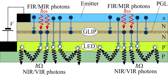
Figure 1 shows the PGLIP-LED device structure with a single PGL sandwiched by the N-barrier layers and with the top emitter n-layer. The structure comprises also the p+-layer (on the P-type substrate), which serves as the active region of the LED part of the device. Figures 2(a) - 2(c) show the band diagrams corresponding to different electric field in the emitter barrier layer and in the collector barrier layer . The PGLIP part of the device structure under consideration is somewhat different from those studied in Refs. 12 ; 13 ; 14 ; 15 , where the emitter n-layer is assumed to be a GL.
Under the bias voltage applied between the n-emitter and p+-collector layer (serving as the LED active region), the electron tunneling through the triangular barrier provides the electron injection from the emitter to the barrier layer between the n-emitter region and the PGL. A portion of the injected electrons crosses the PGL and enters to the collector barrier layer and than to the p+-layer. The electron tunneling or thermionic emission from the PGL also contribute to the net current collected by the p-layer. The incident FIR/MIR spatially nonuniform in the device plane generates the spatially nonuniform electron photocurrent from the PGL. It is associated with the electrons photoexcited in the PGL from its valence band into the conduction band (see Figs. 1 and 2) which go to the barrier layer either directly or after the tunneling through the triangular barrier between the PGL and the collector barrier layer (depending on the FIR/MIR photon energy and the height of the barrier between the PGL and the collector barrier layer). The spatial distribution of the photocurrent from the PGL repeats the spatial distribution of the incident FIR/MIR. The photoexcitation of the PGL leads to the deviation of its potential from its dark value . If the PGL lateral resistivity is relatively low (as in sufficiently perfect and/or doped GLs), is virtually independent of the lateral coordinates, so that the variation of the photocurrent injected from the emitter is uniform as well. Thus, in such a case, the nonuniform irradiation leads to the nonuniform current generated solely from the PGL, whereas the net photocurrent is produced by both the PGL and the emitter. Similar situation occurs in the pixelless QWIP-LED image up-converters due to low QW lateral resistivity. The latter can not normally be made sufficiently high because of the necessity to maintain relatively high electron concentration (doping) in the near emitter QW to provide a sufficient intersubband absorption and photoemission. In contrast, in the PGLIP-LED devices, the lateral resistivity of the PGL can be so high that the nonuniform distributions of the photogenerated holes (left in the PGL after the escape of the photoelectons) do not manage to relax. Hence in this case, the PGL electric potential spatial distribution becomes similar to that of the incident radiation. This results in the nonuniform density of the photocurrent emitted not only from the PGL but also injected from the n-emitter. As a result, the spatially nonuniform component of the net current stimulated by the incident FIR/MIR can be larger than the component associated with the photoemission from PGL solely. In other words, the effect of photoconductive gain amplifies not only spatially uniform currents (the dark current and the current generated by the averaged component of the incident FIR/MIR intensity ) but the ”image” component as well.
The PGLIP-LED image up-converter model accounts for the main processes responsible for the device operation, namely, the electron photoemission from the PGL (direct and followed by tunneling), capture of the electrons injected from the emitter into the PGL, processes of the PGL lateral conductivity, injection of the photocurrent to the LED active layer, and the lateral electron propagation due to the diffusion and the reabsorption (recycling) of the NIR/VIR photons trapped in this layer. The main feature of the device under consideration is the use of large area polycrytalline GL as a photosensitive element with decreased dc conductivity.
In the absence of irradiation, the densities of the electron tunneling current from the emitter and the current of the electrons photoescaped from the PGL, and , respectively, can be presented as and . Here and are the maximum electron current densities, which can be extracted from the emitter n-layer and the PGL. These quantities are determined by the doping and the electron try-to-escape times. The characteristic tunneling fields for the near-equilibrium electrons in the n-emitter and for the photoexcided electronsin the PGL are equal to and 48 , respectively, where and are the electron activation energies in the n-emitter layer and the GL, is the electron effective mass in the barrier layers, is the electron charge, and is the Planck constant. The emitter and collector fields and satisfy the equation , were and are the thicknesses of the barrier layers and is the bias voltage. In the following, to avoid to cumbersome formulas we, for simplicity, set and .
Equalizing the capture rate of the injected electrons crossing the PGL into the latter , where or is the capture probability (capture parameter) of an electron crossing the PGL into it 5 ; 7 ; 8 ; 9 ; 11 ; 12 ; 13 ; 14 ; 15 , and the rate of the electron tunneling escape from the GL , one can find in the case of the undoped GL, which will be primarily considered in the following, the condition
| (1) |
is achieved at with
| (2) |
In the situation under consideration, the surface charge in the PGL , so that the PGL Fermi level coincides with the Dirac point, carrier density is minimized, that promotes an elevated GL resistivity. Such a situation can take place when , i.e., when . The latter inequality implies that , where is the electron Fermi in the emitter. Here and are the differences between the electron affinities of the emitter material () and of the PGL () and that of the barrier material . Hence, the structure materials and the emitter doping should be chosen in a such a way that and .
The deviation of from leads to or and to the formation of the excess electron or hole charges in the undoped GL. Usually the latter can result in a marked drop of the GL resistivity. If the PGL is doped, the appropriate choice of the bias voltage , can decrease the carrier density and, hence, increase the GL resistivity. In this case, , although the PGLIP-LED characteristics can be found analogously.
The consequences of the departure of the GL electron-hole system from the Dirac point will be discussed below.
To provide an effective injection of the electrons from the GLIP part to the p-layer in the LED part and NIR/VIR emission from the latter, the following two conditions should be fulfilled: (1) absence of the barrier at the p-layer and (2) sufficiently large band gap in the latter layer (to secure emission of the NIR/VIR photons). The first condition requires .
III Current output from the GLIP
The intensity of the incident FIR/MIR with the frequency and the variation of the GL potential caused by irradiation comprise the spatially averaged and spatially nonuniform (in the in-plane -direction) components:
| (3) |
Here is the wavenumber characterizing the scale of the image details. The components o of the injected current density induced by the incident FIR/MIR (photocurrent density) are given by
| (4) |
where is the differential conductance of the emitter. The spatially uniform components and can be found accounting for the balance of the electron captured into and photoescaped from the GL. As a result,
| (5) |
with the quantity
| (6) |
describing the dependence of the electron photoescape on the FIR/IR photon energy 12 ; 13 ; 14 ; 15 , , is the fine structure constant and is the barrier material refractive index.
Taking into account the spreading of the holes photogenerated in the PGL due to the lateral conductivity of the latter, the spatially nonuniform components of the PGL potential can be derived using the following equation (the continuity equation):
| (7) |
Here is the parameter characterizing the lateral spreading of the GL potential and is the GL resistivity.
Equations (4) and (7) yield
| (8) |
so that the spatially nonuniform component of the electron current density from the emitter reads
| (9) |
Considering that the fraction of the electrons injected from the emitter and crossed the PGL is equal and that the spatially uniform and nonuniform components of the electron current density emitted from the PGL are, respectively, given by
| (10) |
| (11) |
for the components of the electron photocurrent density injected to the p+-layer, one can obtain
| (12) |
| (13) |
The first term in the brackets in Eqs. (12) and (13) are due to the contribution of the photoelectric gain effect. When the GL lateral conductivity increased, the parameter tends to zero, so that the photoelectric gain effect for the nonuniform current vanishes.
If tends to zero, Eqs. (12) and (13) become similar to the pertinent equation in Ref. 12 . Some distinctions are associated with different photosensitivity of the emitter contacts.
The effect of photoconductive gain becomes substantial when . Depending on the emitter differential conductance, capture probability, GL lateral mobility, the parameter can vary in a wide range. Let us estimate the ratio for cm-1, corresponding to the FIR/MIR with the wavelength m.
Using Eqs. (12) and (13), the photocurrent densities and can be expressed via the PGLIP characteristic responsivity
| (14) |
This yields
| (15) |
| (16) |
If eV, eV, A/cm2, ( is the mass of bare electron), and , one obtains V/cm, V/cm, V/cm, and A/Vcm. At eV and eV, one obtains V/cm, V/cm, V/cm, and A/Vcm. Using these data, setting cm and k, we find cm-1 and cm-1, respectively. This implies that to achieve the ratio for , corresponding to the incident FIR with the wavelength m, one needs to use the GLs with the resistivity much larger than k.
The radiative recombination of the electrons injected to the LED p-layer with the holes provides the emission of NIR/VIR photons with the energy , where is the energy gap of the p-layer. The intensity of the output NIR/VIR stimulated by the incident FIR/MIR is determined by the internal quantum efficiency (where and are the times of nonradiative and radiative recombination, respectively) and by the fraction of the generated NIR/VIR photons trapped in the LED p-layer due to total internal reflection .
Considering the electron diffusion in the p+-LED layer and the effect of recycling of the NIR/VIR photons 49 ; 50 ; 51 ; 52 ; 53 in this layers, the density of the electrons produced by the photocurrent , which comprises the uniform and spatially nonuniform components, can be found as in Refs. 8 ; 52 ; 53 :
| (17) |
| (18) |
Here and are the interband absorption coefficient of the NIR/VIR photons and the electron diffusion length in the LED p+-layer. Using Eqs. (17) - (18), we obtain
| (19) |
| (20) |
Here characterizes the ratio of the NIR/VIR photons leaving the LED out of it and those entering to the GLIP ( depends on the ratios of the refractive indices of the LED p-layer and the surrounding layers.
IV Derivation of up-conversion characteristics
Substituting and from Eqs. (15) and (16) to Eqs. (19) and (20), for the pixelless PGLIP-LED average up-conversion and image up-conversion efficiencies defined as
respectively, we arrive at the following formulas:
| (21) |
| (22) |
Here
| (23) |
| (24) |
| (25) |
The function describes the role of the GL lateral potential spreading with decreasing of the nonuniformity scale.
The image contrast transfer function, i.e., the ratio of the conversion efficiencies of the image nonuniform component to its averaged value
which characterizes the output NIR/VIR image contrast, as follows from Eqs. (21) and (22) is described by
| (26) |
V Results


The plots based on the above calculations of the up-conversion characteristics are shown in Figs. 3 - 6. For the definiteness, the following device parameters are assumed: and A/Vcm, , cm, , and . Other parameters are indicated below.
Figure 3 shows the dependence of the the PGL lateral potential spreading factor on the image wavenumber calculated using Eq. (24) for different values of the capture probability and the PGL resistivity . One can see that a decrease in the capture probability (leading to an increase of the photoconductive gain and, therefore, in the enhancement of the role of the nonuniform injection from the emitter), can markedly suppress the lateral potential spreading. An increase in the PGL resistivity also promotes the latter (compare the solid and dashed lines in Fig. 3).
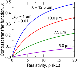
Figure 4 shows the image contract transfer function versus the image wavenumber calculated for different PGL resitivities and electron diffusion length in the LED p-layer . The pertinent calculations are based on Eqs. (22) -(26). The following parameters are assumed: , , and m-1. In particular, Fig. 4(a) indicates an improvement of the contrast of the NIR/VIR image when the PGL resistivity rises. This is due to the pertinent suppression of the PGL potential spreading shown in Fig. 3. As follows from Fig. 4(b), a weaker lateral diffusion of the electrons injected into the LED p+-layer also promotes better contrast.
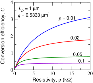
Plots of and shown in Figs. 5 and 6 indicate that using the PGLs with higher resistivity improves the output image contrast and increases the energy conversion efficiency. Diminishing the photon recycling effect in the LED (characterized by parameters and in Eqs. (25) and (26)), which attenuates the effective electron diffusion,also leads to a higher quality of the output image.
Figure 6 corresponds to eV, eV, m-1, , , and other parameters as in the above figures. As seen from Fig. 6, the energy conversion efficiency can markedly exceed unity. The optimization of the parameters, first of all the LED parameters (increase in the internal and external LED efficiencies), might provide even higher values of the PGLIP-LED energy conversion efficience than those in Fig. 6.
As follows from Figs. 4(a), 5, and 6, the PGLIP-LED up-converter characteristics improve with increasing PGL lateral resistivity . This is attributed to the increasing role of the photoconductive gain when the resistivity rises (see below). Using PGLs with small grain sizes 41 ; 42 (see also Refs. 43 ; 44 ; 45 ; 46 ; 47 ), one can realize the resistivities much higher than those considered in the above figures (say, 500 k at nm).
As mentioned in Sec. II, a deviation of from zero leads to violation of condition (1) and, hence, to a decrease in the GL responsivity due to the deviation of the Fermi level in the GL from the Dirac point. A decrease in the resistivity with increasing carrier density in the PGL is complicated by the mobility density dependence and the specifics of the inter-grain transport. Deviation of the voltage from the that corresponding to the Dirac (neutrality) point in rather wide range might lead to a decrease of the PGL resistivity by several times41 . This, can result in a marked decrease in the contrast transfer function and the conversion efficiency (see Figs. 5 and 6, respectively).
VI Materials for PGLIP-LED devices
Different materials can be used for the PGLIP-LED layered structures, providing their proper relations between the electron affinities (see, in particular, Refs.54 ; 55 ).
For example, the PGLIP section can include:
(a) n-Si emitter, SiO2 or hBN -emitter barrier, WS2 collector barrier (as in GL-based vertical-field effect
transistors 22 );
(b) the n-Si emitter, Si02 emitter barrier layer (as in GL-based hot electron transistors 57 ; 58 ; 59 )
and Si collector barrier layer;
(c) the Ti-base emitter, Al2O3 emitter barrier layer, and Si collector barrier layer
(the material of the LED active layer should have the electron affinity and energy gap larger than that in Si);
(d) As an option,
the emitter layer can also be an n-type GL (as considered in Refs. 12 ; 13 ; 14 ).
VII Discussion
VII.1 Effect of photoconductive gain
The electron photoemission from the PGL leads not only to the photocurrent generation but also (due to the PGL charging and the consequent variation of its potential) to the injection of extra electrons from the emitter. The latter results in a higher net photocurrent in comparison with the photocurrent provided solely by the photoemission from the PGL that constitutes what is usually called as the effect of the photoconductive gain. The photoconductive gain is described by the factor in Eqs. (22) and (26). As follows from this factor definition given by Eq. (24), at tending to zero the factor tends to unity. This is because at small values of , the PGL is virtually equipotential. This implies that in the limit , the photoconductive gain of the nonuniform photocurrent component vanishes, so that the nonuniformity of the photocurrent injected to the LED p+ layer and, hence, the nonuniformity of the output radiation intensity are associated only with the electrons photoexcited from the PGL. Simultaneously, the uniform (averaged) component still can exhibit a substantial gain, i.e., such a component comprises not only the photocurrent created by the electrons photoexcited from the PGL but also by the photocurrent associated with the extra electrons injected from the emitter. This, in particular, seen from Eqs. (21), (22), and (24), where , while does not contain a large factor (in the limit ). As a consequence, at small values of , the contrast transfer function becomes very small () as it seen in Figs. 5 and 6. The same happens in the QWIP-LED image up-converters with a single QW, because this QW inevitably must be highly conducting (i.e., have a small QW resistivity ) to provide the carrier density sufficient for a reasonable photosensitivity.
In the multiple-PGL devices, the spatially uniform and nonuniform components of the photocurrent output from the PGLIP with the resistive PGLs are virtually independent of the number of the PGLs . Hence, in such multiple-PGL devices with all resistive PGLs, the photoelectric gain and almost all PGLIP-LED characteristics are close to those of the PGLIPs with a single PGL. However, the GLIP-LED image up-converters can exhibit lower noise (by a factor of (see, for example, Refs. 34 ).
VII.2 PGLIP-LED versus QWIP-LED
Comparing the image up-conversion efficiency of the PGLIP-LEDs with a single PGL, given by Eqs. (21) - (24), with that of the QWIP-LED imagers 5 ; 8 (assuming the same properties of the LED sections), we find
| (27) |
Here , , , and are the cross-section of the photon absorption and the electron density in the QW, the electron capture probability onto the QW, and the number of the QWs in the QWIP. It is assumed for simplicity that the LED sections of both image up-converters have the same characteristics, the number of the QWs is not too large (say, several thens or less), the GL resistivity and the scale of the image nonuniformities are sufficiently large , where , and are the electron diffusion length, electron diffusion coefficient, and drift velocity in the barrier layers. Both factors in the right-hand side of Eq. (27) are large or very large.
Analogously, for the ratio of the image contrast transfer functions of the PGLIP-LED and QWIP-LED one obtains
| (28) |
Due to small values of the capture probability even at a relatively large but practical number of the QWs, the ratio exceeds unity.
VII.3 Role of lateral diffusion of the injected electrons in the barrier layers
In Eqs. (8) and (27) we disregarded the lateral diffusion of the electrons propagating above the barriers (in contrast to Ref. 5 ; 8 ). This is justified because the lateral displacement of these electrons during their rather short flight across the barrier layers is very small. Indeed, such a displacement . Setting cm, cm2/s, and cm/s, we obtain cm, i.e., the value negligibly small in comparison with the incident radiation wavelength.
VII.4 Role of the GL and barriers doping (electrical and chemical)
When the bias voltage deviates from the characteristic voltage , the Fermi energy in the PGL shifts with respect to the Dirac point. This leads to the following consequences. First, an increase in the electron or hole density results in the increase in the GL lateral conductivity and, hence, in the smoothening of the lateral potential distribution and the suppression of the photoelectric gain. The same occurs when the GL is chemically doped.
Second, the Fermi energy shift affects the PGL absorption spectrum due the Pauli principle (toward higher energies of the FIR/MIR photons 15 ). This might be used for a voltage control of the spectral characteristics (say, for the ”filtering”) of the incident FIR/MIR.
Third, the deviation of from as well as chemical doping (giving rise to the formation of the hole gas in the GLIP) can be used for a lowering of the GLIP dark current and, therefore for decrease in the background uniform component of the output NIR/VIR.
VII.5 Optical feedback
If a substantial portion of the NIR/VIR photons generated in the LED active p+-layer (and not reflected by the PGLIP collector barrier) enters the PGLIP (the pertinent wavy arrows are not shown in Figs. 1 and 2), the interband absorption of these photons in the PGLIP (in the GL) leads to an extra photocurrent, which further reinforces the emission of the NIR/VIR photons. Such a positive optical feedback can reinforce not only the average up-conversion efficiency 12 but the image up-conversion as well.
VIII Conclusions
We reported on the proposal of the pixelless FIR/MIR to NIR/VIR up-converter based on the vdW heterostructures with the highly resistive (polycrystalline) PGLs - PGLIP-LED upconverter. Using the developed device model which accounts for generation of nonuniform photocurrent in the GLIP section by FIR/MIR, the photocurrent injection to the LED section, and emission of NIR/VIR from the latter section, we calculated the PGLIP-LED characteristics (the image contrast transfer function and the conversion efficiency). The photocurrent lateral spreading was considered taking into account the PGL lateral conductivity and the effective diffusion of the electrons injected into LED (combining their standard diffusion and the lateral spreading due to the photon recycling). We showed that the pixelless PGLIP-LED up-converters can be effective imaging devices exhibiting the power image up-conversion efficiency substantially exceeding unity. Recent publications 54 ; 55 ; 56 ; 57 and others support the feasibility of realization of the PGLIP-LED devices with elevated performance. The proposed and evaluated pixelless PGLIP-LED up-converters can markedly surpass the pixelless QWIP-LED imagers.
Acknowledgments
The authors are grateful to D. Svintsov, V. Leiman, V. Mitin, and A. Satou for useful information and numerous discussions. The work at RIEC and UoA was supported by the Japan Society for Promotion of Science, KAKENHI Grant No. 16H06361. The work at BMSTU was supported by the Russian Scientific Foundation, Grant No. 14-29-00277. VR and MS acknowledge the support by the Russian Foundation for Basic Research, Grant No.16-37-60110/16 and by the US ARL Cooperative Research Agreement, respectively.
References
- (1) S. Baldelli,Sensing: Infrared image upconversion, Nat. Photon. 5 (2001) 75-76.
- (2) M. F. Duarte, M. A. Davenport, D. Takhar, J. N. Laska, T. Sun, K. F. Kelly, and R. G. Baraniuk, Single-pixel imaging via compressive sampling, IEEE Signal Processing Mag. 83 (2008) 83–91.
- (3) G. Overton, Photonics applied: photovoltaic sistems: Optics take center stage in concentrating photovoltaic systems, Laser Focus World, 17 Feb. (2010).
- (4) T. N. Singh-Rachford and F. N. Castellano, Photon upconversion based on sensitized triplet-triplet annihilation, Coordination Chem. Rev. 254 (2010) 2560-2573.
- (5) V. Ryzhii, H. C. Liu, I. Khmyrova, and M. Ryzhii, Analysis of integrated quantum-well IR photodetector and light-emitting diode for implementing pixelless imaging devices, IEEE J. Quantum Electron. 33 (1997) 1527–1531.
- (6) H. C. Liu, L. B. Allard, M. Buchanan, and Z. R. Wasilewski, IR imaging device, Electron. Lett. 33 (1997) 379–380.
- (7) L. B. Allard, H. C. Liu, M. Buchanan, and Z. R. Wasilewski, Pixelless IR imaging utilizing a p-type quantum well IR photodetector integrated with a light emitting diode, Appl. Phys. Lett. 70 (1997) 2784–2786.
- (8) V. Ryzhii, I. Khmyrova, and P. Bois, Photon mechanism of image smearing in integrated QWIP-LED pixelless devices, IEEE J. Quantum Electron. 35 (1999) 1693–1696.
- (9) S. Oktybrsky, I. Khmyrova, and V. Ryzhii, Characteristics of integrated QWIP-HBT-LED up-converters, IEEE Trans. on Electron Devices 50 (2003) 2378–2387.
- (10) A. Rogalski, Infrared Detectors, Second Edition, (CRC Press, 2011).
- (11) H. C. Liu, E. Dupont, M. Byloos, M. Buchanan, C.-Y. Song, and Z. R. Wasilewski, QWIP-LED pixelless thermal imaging device, in Intersubband Infrared Photodetectors ed.V.Ryzhii (World Scientific, 2003), pp.299-314.
- (12) V. Ryzhii, T Otsuji, M. Ryzhii, V. E. Karasik, and M. S. Shur, Infrared detection and photon energy up-conversion in GLIP-LED integrated devices based on van der Waals heterostructures, Infrared Phys. Technol. 85C (2017) 307-314 .
- (13) V. Ryzhii, M. Ryzhii, D. Svintsov, V. Leiman, V. Mitin, M. S. Shur, and T. Otsuji, Infrared photodetectors based on graphene van der Waals heterostructures, Infrared Phys. Technol. 84 (2017) 72–81.
- (14) V. Ryzhii, M. Ryzhii, D. Svintsov, V. Leiman, V. Mitin, M. S. Shur, and T. Otsuji, Nonlinear response of infrared photodetectors based on van der Waals heterostructures with graphene layers, Opt. Express 25 (2017) 5536–5549.
- (15) V. Ryzhii, M. Ryzhii, V. G. Leiman, V. Mitin, M. S. Shur, and T. Otsuji, Effect of doping on the characteristics of infrared photodetectors based on van der Waals heterostructures with multiple graphene layers, J. Appl. Phys. 122 (2017) 045505.
- (16) V. Ryzhii, The theory of quantum-dot infrared phototransistors, Semicond. Sci. Technol. 11 (2016) 759–765.
- (17) V. Ryzhii and I. Khmyrova, Electron and photon effects in imaging devices utilizing quantum dot infrared photodetectors and light-emitting diodes, Proc. SPIE 3948, Photodetectors: Materials and Devices V, (2000) 206–219.
- (18) A. Teitelboim and D. Oron, Broadband near-infrared to visible upconversion in quantum dot–quantum well heterostructures, ACS Nano 10 (2016) 446–-452.
- (19) M. Wu, D. N. Congreve, M. W. B. Wilson, et al., Solid-state infrared-to-visible upconversion sensitized by colloidal nanocrystals, Nat. Photonics 10 (2016) 31–34.
- (20) M. Wu, J. Jean, V. Bulović, and M. A. Baldoa, Interference-enhanced infrared-to-visible upconversion in solid-state thin films sensitized by colloidal nanocrystals, Appl. Phys. Lett. 110 (2017) 211101.
- (21) A. K. Geim and I. V. Grigorieva, Van der Waals heterostructures, Nature 499 (2013) 419–425.
- (22) T. Georgiou, R. Jalil, B. D.Belle, L. Britnell, R. V. Gorbachev, S. V. Morozov, Y.-J. Kim, A. Gholinia, S. J. Haigh, O. Makarovsky, L. Eaves, L. A. Ponomarenko, A. K. Geim, K. S. Novoselov, and A. Mishchenko, Vertical field– effect transistor based on graphene–WS2 heterostructures for flexible and transparent electronics, Nat. Nanotechnol. 7 (2013) 100–103.
- (23) L. Britnell, R. V. Gorbachev, A. K. Geim, L. A. Ponomarenko, A. Mishchenko, M. T. Greenaway, T. M. Fromhold, K. S. Novoselov, and L. Eaves, Resonant tunneling and negative differential conductance in graphene transistors, Nat. Commun. 4 (2013) 1794–1799.
- (24) F. Xia, H. Wang, Di Xiao, M. Dubey, and A. Ramasubramaniam, Two dimensional material nanophotonics, Nat. Photon. 8 (2014) 899–907.
- (25) G. W. Mudd, S. A. Svatek, L. Hague, O. Makarovsky, Z. R. Kudrynsky, C. J.Mellor, P. H. Beton, L. Eaves, K. S. Novoselov, Z. D. Kovalyuk, E. E. Vdovin, A. J. Marsden , N. R. Wilson, and A. Patane, High broad-band photoresponsivity of mechanically formed InSe graphene van der Waals heterostructures, Advanced Mat. 27 (2015) 3760–3766.
- (26) Q. Ma, T. I. Andersen, N. L. Nair, N. M. Gabor, M. Massicotte, C. H. Lui, A. F. Young , W. Fang, K. Watanabe, T. Taniguchi, J. Kong, N. Gedik, F. H. L. Koppens, and P. Jarillo-Herrero, Tuning ultrafast electron thermalization pathways in a van der Waals heterostructure, Nat.Phys. 12 (2016) 455–459.
- (27) M. Massicotte,P. Schmidt,F. Vialla,K. G. Schadler, A. Reserbat-Plantey, K. Watanabe, T. Taniguchi, K. J. Tielrooij, and F. H. L.Koppens, Picosecond photoresponse in van der Waals heterostructures, Nat. Nanotech. 11 (2016) 42–46.
- (28) F. Withers, O. Del Pozo-Zamudio, A. Mishchenko, A. P. Rooney, A. Gholinia, K. Watanabe, T. Taniguchi, S. J. Haigh, A. K. Geim, A. I. Tartakovskii, and K. S. Novoselov, Light-emitting diodes by band-structure engineering in van der Waals heterostructures, Nat. Mat. 14 (2015) 301–306.
- (29) F. Withers, O. Del Pozo-Zamudio, S. Schwarz, S. Dufferwiel, P. M. Walker, T. Godde, A. P. Rooney, A. Gholinia, C. R. Woods, P. Blake, S. J. Haigh, K. Watanabe, T. Taniguchi, I. L. Aleiner, A. K. Geim, V. I. Falko, A. I. Tartakovskii, and K. S. Novoselov, Light-emitting tunneling transistors with enhanced brightness at room temperature, Nano Lett. 15 (2015) 8223–8228.
- (30) X. Wang and F. Xia, Van der Waals heterostructures: Stacked 2D materials shed light, Nat. Mat. 14 (2015) 264–265
- (31) J. Binder, F. Withers, M.R. Molas, C. Faugeras, K. Nogajewski, K. Watanabe, T. Taniguchi, A. Kozikov, A.K. Geim, K.S. Novoselov, and M. Potemski, Sub-bandgap voltage electroluminescence and magneto-oscillations in a WSe2 light-emitting van der Waals heterostructure, Nano Lett. 17 (2017) 1425–1430.
- (32) A. H. Castro Neto, F. Guinea, N. M. R. Peres, K.S. Novoselov, and A. K. Geim, The electronic properties of graphene, Rev. Mod. Phys.81 (2009) 109–162.
- (33) F. Rosencher, B. Vinter, F. Luc, L. Thibaudeau, P. Bois, and J. Nagle, Emission and capture of electrons in multiquantum-well structures, IEEE J. Quantum Electron. 30 (1994) 2875–2888.
- (34) K. K. Choi, Physics of Quantum Well Infrared Photode- tectors (World Scientific, 1997).
- (35) H. Schneider and H.C.Lui, Quantum Well Infrared Photodetectors (Springer, 2007).
- (36) V. Ya. Aleshkin, A. A. Dubinov, M. Ryzhii, and V. Ryzhii, Electron capture in van der Waals graphene-based heterostructures with WS2 barrier layers, J. Phys. Soc. Japan 84 (2015) 094703.
- (37) E. O. Polat, O. Balci, N. Kakenov, H. B. Uzlu, C, Kocabas, and R, Dahiya, Synthesis of large area graphene for high performance in flexible optoelectronic devices. Sci. Rep. 5 (2015) 16744.
- (38) S. Bae, H. Kim, Y. Lee, X. Xu, J.-S. Park, Yi Zheng, J. Balakrishnan, T. Lei, H. Ri Kim, Y. Il Song, Y.-J. Kim, K. S. Kim, B, Özyilmaz, J.-H. Ahn, B. H. Hong, and S. Iijima, Roll-to-roll production of 30-inch graphene films for transparent electrodes, Nat. Nanotech. 5 (2010) 574–-578.
- (39) C.-C. Tang, M.-Y. Li, L. J. Li, C. C. Chi, and J.-C. Chen, Graphene-GaAs/AlxGa1−xAs heterostructure dual-function field-effect transistor, Appl. Phys. Lett. 101 (2012) 202104.
- (40) G. Ruhl, S. Wittmann, M. Koenig1, and D. Neumaier, The integration of graphene into microelectronic devices Beilstein J. Nanotechnol. 8 (2017) 1056–1064.
- (41) A. W. Cummings, D. L. Duong, V. L. Nguyen, D. V. Tuan, J. Kotakiski, J.E.V. Vargas, Y. H. Lee, and S. Roche, Charge transport in polycrystalline graphene: Challenges and opportunities, Adv. Mater. 26 (2014) 5079-5094.
- (42) I. Vlassiouk, S. Smirnov, I. Ivanov, P. F Fulvio, S. Dai, H. Meyer, M. Chi, D. Hensley, P. Datskos, and N. V Lavrik, Electrical and thermal conductivity of low temperature CVD graphene: the effect of disorder, Nanotechnology 22 (2011) 275716.
- (43) O. V. Yazyev and S. G.Louie, Electronic transport in polycrystalline graphene, Nat. Mat. 9 (2010) 806–809.
- (44) , Y. Liu and B. T. Yakobson, Cones, pringles, and grain boundary landscapes in graphene topology, Nano Lett. bf 10 (2010) 2178.
- (45) A. W. Tsen, L. Brown, M. P. Levendorf, F. Ghahari, P. Y. Huang1, R. W. Havener, C, S. Ruiz-Vargas1, D. A. Muller1, Ph. Kim, and J. Park, Tailoring electrical transport across grain boundaries in polycrystalline graphene, Science 336, (2012) Issue 6085, 1143–1146.
- (46) D. V. Tuan, J, Kotakoski, T. Louvet, F. Ortman, J. C. Meyer, and S. Roche, Scaling properties of charge transport in polycristalline graphene, Nano Lett. 13 (2013) 1730–1735.
- (47) J. E Barrios Vargas, J. T. Falkenberg, D. Soriano1, A. W Cummings, M. Brandbyge, and S. Roche, Grain boundary-induced variability of charge transport in hydrogenated polycrystalline graphene, 2D Mater. 4 (2017) 025009.
- (48) S. M. Sze, Physics of Semiconductor Devices (Wiley,1999), p.103.
- (49) F. Stern and J. M. Wooddall, Self-absorption effects on the radiative lifetime in GaAs‐GaAlAs double heterostructures, J. Appl. Phys. 45 (1974) 3904–3906.
- (50) I. Schnitzer, E. Yablonovich, C.Caneau, and T. J. Gmitter, Ultrahigh spontaneous emission quantum efficiency, 99.7 internally and 72 externally, from AlGaAs/GaAs/AlGaAs double heterostructures, Appl. Phys. Lett. 62 (1993) 131–133.
- (51) T. Baba, R. Watanabe, K. Asano, F. Koyama, and K. Iga, Theoretical and experimental estimations of photon recycling effect in light emitting devices with a metal mirror, Jpn. J. Appl. Phys. 35 (1996) 97–101.
- (52) N. Tsutsui, I. Khmyrova, V. Ryzhii, and T. Ikegami, Analysis of photon recycling in light emitting diodes with nonuniform injection, J. Appl. Phys. 88 (2000) 3613–3617.
- (53) N. Tsutsui, I. Khmyrova, V. Ryzhii, and T. Ikegami, Effect of photon recycling in pixelless imaging device, Jpn. J. Appl. Phys. 39 (2000) 5080–5082.
- (54) G. Gong, H. Zhang, W. Wang, L. Colombo, R. M. Wallace, and K. Cho, Band alignment of two-dimensional transition metal dichalcogenides: Application in tunnel field effect transistors, Appl. Phys. Lett. 103 (2013) 053513.
- (55) J. Kang, S. Tongay, J. Zhou, J. B. Li, and J. Q. Wu, Band offsets and heterostructures of two-dimensional semiconductors, Appl. Phys. Lett. 102 (2013) 012111.
- (56) A. Zubair, A Nourbakhsh, J. Y. Hong, M Qi, Y Song, D. Jena, J. Kong, M. S. Dresselhaus, and T. Palacios, Hot electron transistor with van der Waals base-collector heterojunction and high performance GaN emitter, Nano Lett., April 17 (2017).
- (57) S.Vaziri, G. Lupina, C. Henkel, A. D. Smith, M. Osling, J. Dabrowski, G. Lippert, W. Mer, and M. C. Lemme, A graphene-based hot electron transistor, Nano Lett. 13 (2013) 1435–1439.
- (58) C. Zeng, E. B. Song, M. Wang, S.Lee, C. M. Torres, Jr., J. Tang, B. H. WEiler, and K. L. Wang. Vertical graphene-base hot-electron transistor, Nano Lett. 13 (2013) 2370–2375.
- (59) H. G. Lee, S. J. Kim, Il-S. Kang, G. S. Lee, K. N. Kim, and J.W. Koh, Characterisation of hot electron transistors using graphene base, J. Korean Inst. Electr. Electron. Mater. Eng. 29 (2016) 147–151.