Janus: An Uncertain Cache Architecture to Cope with Side Channel Attacks
Abstract
Side channel attacks are a major class of attacks to crypto-systems. Attackers collect and analyze timing behavior, I/O data, or power consumption in these systems to undermine their effectiveness in protecting sensitive information. In this work, we propose a new cache architecture, called Janus, to enable crypto-systems to introduce randomization and uncertainty in their runtime timing behavior and power utilization profile. In the proposed cache architecture, each data block is equipped with an on-off flag to enable/disable the data block. The Janus architecture has two special instructions in its instruction set to support the on-off flag. Beside the analytical evaluation of the proposed cache architecture, we deploy it in an ARM-7 processor core to study its feasibility and practicality. Results show a significant variation in the timing behavior across all the benchmarks. The new secure processor architecture has minimal hardware overhead and significant improvement in protecting against power analysis and timing behavior attacks.
I Introduction
Computing and embedded systems have penetrated almost every aspect of our daily lives, from mobile phones and artificial pacemakers to thermostats and self-driving vehicles. In fact, nowadays, most of the integrated circuits (ICs) in use are found in embedded systems and processing sensitive information. The need to improve the security of these systems has never been greater because of the ongoing push to connect them to the Internet. To meet some of the security challenges, different crypto-systems have been proposed. However, one of the common attacks on crypto-systems, and computing systems in general, is side channel attacks (SCAs) in which external indicators such as power consumption and electromagnetic emissions can be used to derive secret and sensitive information. Power analysis attacks, fault injection attacks, and timing attacks are among the most successful side channel attacks. With power analysis attacks, the power expenditure of a crypto-system is investigated by attackers in order to reveal sensitive information such as cryptographic keys. The most popular power analysis attacks are known as simple power analysis (SPA) and differential power analysis (DPA) attacks [1]. In SPA attacks, the power consumption graphs related to the electrical activities of the IC modules are interpreted visually. With DPA techniques, attackers collect and analyze data from various cryptographic functions, and use them to calculate the intermediate values of cryptographic computations. Since power consumption monitoring is not invasive, the crypto-system may not detect power analysis attacks. To cope with power analysis attacks, the system’s power consumption can be obfuscated. Randomization of the IC runtime power variations is one such technique. By randomizing the consuming power of a crypto-system, attackers find it more difficult to extract secret information. Memory operations and the memory hierarchy can be utilized to randomize the power expenditure. Fault injection attacks are another widely used class of side channel attacks [2]. Fault injection attacks have two main phases. In the first phase, the attacker maliciously injects some faults in order to affect the input parameters, processing unit [3], storage unit [3], or instructions [4] of the crypto-system. In the second phase, an analysis is done to gathered information e.g., I/O data, timing behaviors to reveal secret keys inside the crypto-system. Fault injection attacks are often based on some well-defined analysis vectors [5] performed on the gathered information during attacks. Randomizing the timing and I/O data of a crypto-system significantly improves security of the system, especially, against fault injection attacks [5]. In this work, we propose and evaluate a new cache design to cope with power and fault injection attacks. In the proposed Janus cache architecture, each cacheline has an additional “on-off flag” (OOF) bit to enable and disable access to the data block. By introducing instructions to turn on and off cachelines, the runtime power utilization and the timing behavior of the cache structure are efficiently obfuscated.
II Related Work
In [6], a hardware-software randomized instruction injection scheme (RIJID) was proposed. In RIJID, the power utilization is scrambled so that the segments of the encryption code cannot be identified. The scheme has shown some efficacy against both SPA and DPA attacks that use system power profile to extract encryption code. Ambrose et al. in [7] proposed the use of parallel capability in multi-modulo residue number systems (RNS) architectures to scramble sensitive data. By using RNS architectures, the operations can be divided into parallel sections, and thus, the power consumption and complexity are reduced. Yang et al. [8] introduced a scheme known as random dynamic voltage and frequency scaling (RDVFS) to decrease the correlation between the system power consumption and input data by changing the frequency and voltage randomly. However, RDVFS method cannot defeat SPA/DPA power attacks [8]. In [9], authors developed a policy using dynamic voltage and frequency scaling (DVFS) to overcome the limitations of RDVFS by breaking correlations between voltage and frequency of (V, f) pairs. In [10], the advanced encryption standard (AES) algorithm is implemented using techniques resistant to first order differential electromagnetic and power analyses. With this approach, the Galois Field of the AES is randomized and no additional operation is added to the algorithm. Consequently, the working frequency remains the same and the used algorithm is compatible to the published standard. Fault attack tolerant methods generally fall under one of two categories: fault avoidance and fault protection. In both cases, extra hardware is often required to (a) check and prevent fault injection or (b) rollback the crypto-system to recover from the fault. Most of the proposed approaches dealt with power attacks while ignoring fault attacks or vice versa. In this work, we try to jointly address both fault injection and power attacks in crypto-systems.
III Janus Cache Architecture
In both general-purpose and embedded computing, the overall system’s performance and power usage is highly dependent on the cache’s performance. When the processor needs some data, it goes to the cache. If the data is in the cache, there is a hit. Otherwise, the processor has to wait for main memory to supply the data. Since access time for the main memory is orders of magnitude greater than the cache access time, cache hits and cache misses have very different access times and power profiles. From the power consumption view, a cache hit consumes very little energy since no external lines of data are moved through the memory subsystem hierarchy and no main bus address or data activities are involved. Therefore, the hit rate of the cache system plays a pivotal role in the power consumption and timing behavior of a crypto-system. The key insight is that by changing the miss and hit rates, one can alter the power consumption and timing behavior of the system leading to a more robust crypto-system.
The proposed cache architecture operates under fully associative policy for substituting the data words. More specifically, new data words can be stored in any free locations of the cache, and if the cache is full, data eviction and new data words placement use the Least Recently Used (LRU) policy. In the Janus cache design, for each block of data there is one flag bit called “on-off flag” (oof). The oof is used to enable or disable access to a particular cacheline even when the valid bit of the line is one and there is a match on the tags. By introducing a small set of instructions for turning on and off the oof bits, we are effectively able to (a) obfuscate the power utilization of system in a controlled manner and (b) minimize the hardware modifications needed to support the new security feature. All the fields in the conventional cache structure and their functionalities remain the same. For simplicity, we did not show the cache coherence bits field. The oof bit check happens after the valid bit check, therefore, in the Janus architecture, there is one single gate delay in the cache structure. To control the state of each oof of the cache structure, we introduce two on-off instructions: “cache-block-on-” and “cache-block-off-”, for controlling the -th cacheline. By exploiting these two instructions, the amount of effective hit and miss rates of the cache is controlled beyond the normal miss and hit rates of the executing program. This approach gives users a program level access for controlling the desired amount of obfuscation. The random injection of this instruction pair into the based code creates a runtime power profile and timing behavior for the crypto-system that are more resilient to power analysis and fault injection attacks.
III-A Runtime ON-OFF Algorithm
Each memory request now has three possible outcomes: (1) program miss, (2) program hit and oof off, and finally (3) program hit and oof on. When the addressed block has not been previously brought in the cache or has been evicted, a cache miss occurs. However, if the block is found in the cache, there is a cache hit. Since cachelines can be disabled through the security policy, certain cache misses are intentional (IM) - outcome (2). In the case of an IM, the crypto-system follows the same data fetching process (either from lower caches or main memory) as in the case of a genuine cache miss. To make sure that an IM and an actual miss have the same power and latency profiles, the fetched block is placed on top of the old. Let us assume that the cache has data blocks, from 0 to , and the considered code to be run consists of time slots, from 0 to . Turning off each data block increases the power utilization of the crypto-system. This execution time overhead is based on the amount of IMs encountered during program execution. This increase in power can be modeled as a random variable, more specifically as a Poisson random variable, since it depends on the number of on-off instruction pairs executed at runtime. Let denote the increase in power in the crypto-system when the -th cache data block is turned off. Thus, for , we have:
| (1) |
is the number of active requests on the -th data block during execution and is a constant value (the power consumed by the crypto-system to bring in data from the RAM - Random Access Memory - instead of the cache). With the Janus caching scheme, the execution of on-off instruction pairs and their effects on the cache miss rate add uncertainty to the power consumption of the crypto-system, and obfuscate the actual program execution power usage profile. As a result, the crypto-system is protected against the power analysis attacks. The runtime power utilization uncertainty or the added noise is a random process. In practical systems, the power consumption is capped (i.e., the second moment of the noise is limited), therefore, the highest uncertainty (i.e., entropy) in the power consumption can be realized with a Gaussian noise model [11]. For this reason, the Janus caching scheme creates a Gaussian noise in the power consumption through the random variable and uses it to insert the appropriate number of on-off instruction pairs in the code. Let denote the amount of Gaussian noise at the time slot which can be modeled by a Gaussian random variable. Because of practical limitations, a pure Gaussian random variable cannot be generated, thus, a pseudo Gaussian random variable at the time slot is used. For producing the , at first, we choose two numbers and in the range of arbitrarily. can be produced using the following equations [11]:
| (2) |
If , we select another and until holds. This is the amount of Gaussian noise at the time slot that should be added to the power consumption of the system. Algorithm 1 presents the procedure for achieving the value of in Equation 2 to be added to the random variables in Equation 1. The algorithm derives in by exploring the on and off states of the cache data blocks in the time slot .
It is worth noting that, although we illustrate the Janus architecture with a single level cache for presentation simplicity, it works in multi-level cache systems as well.
IV Evaluations
IV-A Analytical Evaluation
The analytical assessment of the Janus cache architecture focuses on (a) the number of available data blocks to turn on and off in the cache at any given time and (b) the error probability of guessing the consumed power. Let us assume that there are data blocks available to turn on and off, and turning off each of them results in some power increase. During each time slot, there are possible data block states and power difference between them. Based on [12] noise quantization results, the variance of distance between the Pseudo-Gaussian noise produced by turning on and off the data blocks and the Gaussian noise, i.e., , can be calculated as
| (3) |
By increasing the number of available data blocks in the cache structure to be turned on and off, one can decrease the distance between the two noises. Another important metric for evaluating the Janus architecture’s performance is its error probability in estimating the crypto-system’s power usage to the on and off decisions. Since a Gaussian noise model is used, one can model the error probability of the power estimate as the error rate in an additive white Gaussian noise (AWGN) channel using binary phase-shift keying (BPSK) modulation. Using the same approach as in [12] for AWGN channel, the error probability of the estimated power, i.e., , can be written as
| (4) |
Where is the error function and equals to .
IV-B Simulation Results
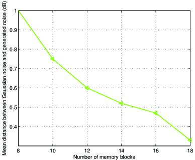
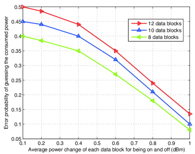
Data blocks are turned on and off in the Janus cache architecture using Algorithm 1. We compare the measured consumed power of the system to the theoretical Gaussian noise model to show that the proposed architecture effectively randomizes the power consumption of the crypto-system. Figure 1(a) shows the mean distance between the Gaussian noise and the produced noise under Janus’ on and off of data block policy. By increasing the number of the data blocks in the cache structure, the average distance between the produced noise and the Gaussian noise is reduced. Figure 1(b) shows the error probability of the estimated power usage as a function of the average power change introduced by data blocks being turned on or off. By increasing the number of data blocks and the average change power of each data block, the error probability of power consumption estimate decreases.
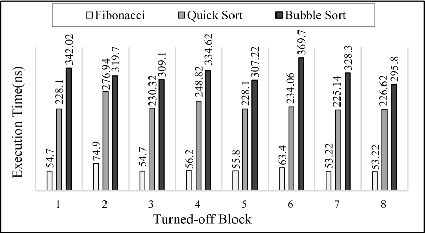
To fully evaluate the concrete and practical implications of the Janus cache architecture on the timing behavior of a crypto-system, we
deploy the Janus architecture in a gate-level synthesized version of the ARM-7 processor that is simulated using the XILINX ISIM simulator. The timing behavior of the synthesized ARM-7 on three
benchmarks (1) Fibonacci sequence generator, (2) quick sort, and (3) bubble sort is extracted and analyzed.
The timing behavior results are reported in Figure 2(a). Depending on the temporal locality of the program, turning off a single
data block in the cache can have a significant effect on the runtime behavior of the system.
A powerful resulting insight from this analysis is the fact that even if an attacker identifies the data block with the most effect on the system
runtime behavior under one program code, this information may not be useful or effective in attacking the same crypto-system running another
program. Therefore moving target security features are also present in the Janus design as a byproduct.
| Mean execution | Execution time | |
|---|---|---|
| time (ns) | variance | |
| Bubble sort | 325.8 | 547.951 |
| Quick sort | 237.26 | 313.49 |
| Fibonacci | 58.26 | 55.67 |
| Mean execution | Execution time | Normal execution | |
|---|---|---|---|
| time (ns) | variance | time (ns) | |
| Bubble sort | 311.86 | 122.11 | 290.220 |
| Quick sort | 238.12 | 88.65 | 223.660 |
| Fibonacci | 58.26 | 55.67 | 51.740 |
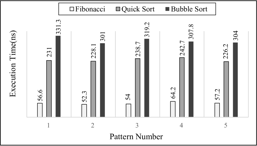
To investigate the effect of turning on and off the data blocks on the program execution profile, we create 5 different patterns, each pattern has 5 time intervals (the first four are 60 nanoseconds long and a last interval runs to the end of the program). For each pattern, at each interval, different cache block sets are turned on and off. Figure 2(b) shows the results of these experiments. The mean and variance of the runtimes for the benchmarks in Figure 2(a) are summarized in Table I. Table II presents the mean and variance of runtimes for benchmarks under the different on-off patterns. The results show that even under this simple time slicing approach, the Janus architecture scrambles the mean and variance of the program runtime enough to provide strong protection against fault injection attacks.
V Conclusion
In this work, we propose a new caching architecture, called Janus, to enable the randomization of the power consumption in crypto-systems. By obfuscating the runtime power profile the Janus architecture is able to effectively protect these systems against power analysis and timing behavior attacks. The Janus cache architecture is deployed in a synthesized ARM-7 processor core running three different benchmarks to evaluate (a) the feasibility of the architecture, and (b) its efficacy against the mentioned attacks.
References
- [1] P. C. Kocher, J. Jaffe, and B. Jun, “Differential power analysis,” in Proceedings of the 19th Annual International Cryptology Conference on Advances in Cryptology, ser. CRYPTO ’99. London, UK, UK: Springer-Verlag, 1999, pp. 388–397.
- [2] P. Kocher, R. Lee, G. McGraw, and A. Raghunathan, “Security as a new dimension in embedded system design,” in Proceedings of the 41st Annual Design Automation Conference, ser. DAC ’04. New York, NY, USA: ACM, 2004, pp. 753–760, moderator-Ravi, Srivaths.
- [3] D. Page and F. Vercauteren, “A fault attack on pairing-based cryptography,” IEEE Transactions on Computers, vol. 55, pp. 1075–1080, 2006.
- [4] S.-M. Yen, S. Kim, S. Lim, and S. Moon, “A countermeasure against one physical cryptanalysis may benefit another attack,” in Proceedings of the 4th International Conference Seoul on Information Security and Cryptology, ser. ICISC ’01. London, UK, UK: Springer-Verlag, 2002, pp. 414–427.
- [5] M. Tunstall, D. Mukhopadhyay, and S. Ali, “Differential fault analysis of the advanced encryption standard using a single fault,” in IFIP International Workshop on Information Security Theory and Practices. Springer, 2011, pp. 224–233.
- [6] J. A. Ambrose, R. G. Ragel et al., “Rijid: random code injection to mask power analysis based side channel attacks,” in Design Automation Conference, 2007. DAC’07. 44th ACM/IEEE. IEEE, 2007, pp. 489–492.
- [7] J. A. Ambrose, H. Pettenghi, D. Jayasinghe, and L. Sousa, “Randomised multi-modulo residue number system architecture for double-and-add to prevent power analysis side channel attacks,” IET Circuits, Devices & Systems, vol. 7, no. 5, pp. 283–293, 2013.
- [8] S. Yang, W. Wolf, N. Vijaykrishnan, D. N. Serpanos, and Y. Xie, “Power attack resistant cryptosystem design: A dynamic voltage and frequency switching approach,” in Proceedings of the Conference on Design, Automation and Test in Europe - Volume 3, ser. DATE ’05. Washington, DC, USA: IEEE Computer Society, 2005, pp. 64–69.
- [9] N. D. P. Avirneni and A. K. Somani, “Countering power analysis attacks usingreliable and aggressive designs,” IEEE Transactions on Computers, vol. 63, no. 6, pp. 1408–1420, 2014.
- [10] M. Masoumi and M. H. Rezayati, “Novel approach to protect advanced encryption standard algorithm implementation against differential electromagnetic and power analysis,” IEEE Transactions on Information Forensics and Security, vol. 10, no. 2, pp. 256–265, 2015.
- [11] J. Proakis and M. Salehi, “Digital communications, (mcgrawhill, new york, 2008),” Google Scholar.
- [12] H. C. v. Tilborg, Encyclopedia of Cryptography and Security. Secaucus, NJ, USA: Springer-Verlag New York, Inc., 2005.