Electronic Structure of Ce-Doped and -Undoped Nd2CuO4 Superconducting Thin Films Studied by Hard X-ray Photoemission and Soft X-ray Absorption Spectroscopy
Abstract
In order to realize superconductivity in cuprates with the T’-type structure, not only chemical substitution (Ce doping) but also post-growth reduction annealing is necessary. In the case of thin films, however, well-designed reduction annealing alone without Ce doping can induce superconductivity in the T’-type cuprates. In order to unveil the origin of superconductivity in the Ce-undoped T’-type cuprates, we have performed bulk-sensitive hard x-ray photoemission and soft x-ray absorption spectroscopies on superconducting and non-superconducting Nd2-xCexCuO4 (, and 0.19) thin films. By post-growth annealing, core-level spectra exhibited dramatic changes, which we attributed to the enhancement of core-hole screening in the CuO2 plane and the shift of chemical potential along with changes in the band filling. The result suggests that the superconducting Nd2CuO4 film is doped with electrons despite the absence of the Ce substitution.
High-temperature superconductivity in cuprates is realized by doping hole or electron carriers into the parent material which has been widely considered to be an antiferromagnetic (AFM) Mott insulator. CuO4 (: rare earth) with the T’-type structure, where Cu takes the square-planar coordination, can be doped with electrons by substituting Ce4+ for . Generally, electron doping by Ce substitutions alone cannot induce superconductivity in bulk crystals of the T’-type cuprates, and an additional procedure of post-growth annealing in a reducing atmosphere is required Tokura1989 . Three distinct microscopic scenarios have been experimentally proposed for the role of the reduction annealing Armitage2010 : i) removal of impurity apical oxygen atoms Radaelli1994 ; Schultz1996 ii) creation of vacancies at the regular oxygen sites Riou2004 ; Richard2004 iii) filling of Cu vacancies Kang2007 . While the exact microscopic effect remains elusive, reduction annealing dramatically suppresses the AFM order Richard2007 ; Horio2016 and reduces quasi-particle scattering Xu1996 , inducing superconductivity in the Ce-doped samples.
Furthermore, it has been demonstrated that thin films of T’-type cuprates can exhibit superconductivity without any Ce doping when properly annealed Tsukada2005a ; Tsukada2005b ; Matsumoto2009b ; Krockenberger2013 . The observed decrease of the -axis parameter by annealing Tsukada2005b ; Matsumoto2009b ; Krockenberger2013 rather than its increase Kang2007 should be attributed to the removal of apical oxygen atoms in these samples Radaelli1994 ; Schultz1996 , as the removal of apical oxygen reduces the repulsion between the CuO2 planes. The large surface-to-volume ratio of thin films helps the thorough removal of impurity oxygen atoms. The observation has cast doubt on the fundamental assumption that the parent compound of the cuprate superconductor is an AFM Mott insulator. Theoretical studies using the local density approximation plus dynamical mean field theory (LDA+DMFT) have indeed predicted that the parent compound of the T’-type cuprates is not a Mott insulator but a Slater insulator in the sense that the AFM order is necessary to open the insulating band gap Das2009 ; Weber2010a ; Weber2010b . When discussing the electronic structure of parent compounds and the phase diagram, however, the possibility should not be overlooked that oxygen reduction affects the carrier concentration. In fact, annealing-induced changes in the Néel temperature Mang2004a and the optical conductivity Arima1993 for bulk Nd2-xCexCuO4 crystals have been interpreted as due to the doping 0.03–0.05 electrons/f.u. Recent angle-resolved photoemission spectroscopy (ARPES) studies on Ce-doped bulk single crystals Horio2016 ; Song2017 and that on insulating Ce-undoped thin films Wei2016 have also shown that the electron concentrations of annealed samples estimated from the Fermi surface area are larger than that expected from the Ce concentrations. To understand the cuprate phase diagram and the electronic states of the parent compounds, it is important to unveil the electron concentration of the superconducting (SC) and non-superconducting (non-SC) Ce-undoped T’-type cuprates.
For that purpose, systematic studies of thin film samples with various Ce concentrations and reduction/oxidization treatments are necessary. However, ARPES measurements on such thin films are hampered by the lack of an in-situ ARPES measurement system combined with a molecular beam epitaxy (MBE) apparatus for the T’-type cuprates, which makes ARPES-quality surfaces available. This is because ARPES is a surface-sensitive technique. In this Letter, we report on measurements of bulk-sensitive hard x-ray photoemission spectroscopy (HAXPES) and soft x-ray absorption spectroscopy (XAS) of SC and non-SC Nd2-xCexCuO4 thin films annealed or oxidized under various atmosphere. By HAXPES, one can measure core-level shifts and hence the chemical-potential shift, which directly probes the doped electron concentration. By annealing Nd2CuO4, we observed dramatic changes in the core-level spectra, which can be explained by the strong modification of core-hole screening in the CuO2 planes and by the chemical-potential shift caused by electron doping. The present results indicate the possibility that the SC Ce-undoped T’-type cuprates are doped with a significant amount of electrons.
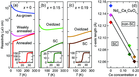
Nd2-xCexCuO4 (, and 0.19) thin films with the thicknesses of 200 nm, 100 nm, and 100 nm, respectively, were grown on SrTiO3 (001) substrates by MBE. For Nd2CuO4, we prepared three kinds of films: as-grown, weakly-annealed, and annealed films, among which only the annealed film showed superconductivity with K. The was defined as the temperature where the resistivity drops to zero. Ce-doped films showed superconductivity without ex-situ annealing in a tubular furnace. The ’s were 24.0 K and 21.5 K for and , respectively. Oxidized non-SC films were also prepared for both the compositions. Conditions of annealing and oxidization are described in Supplementary Information. The resistivity curves and the -axis lengths of all the films are plotted in Fig. 1. The difference in the -axis length between the SC and non-SC films in Fig. 1(d) may largely originate from the difference in the amount of apical oxygen atoms Tsukada2005b ; Matsumoto2009b ; Krockenberger2013 . HAXPES measurements were performed at beamline 47XU of SPring-8 at K with keV photons. The total energy resolution was determined from the Fermi edge of Au to be 0.3 eV. XAS measurements were performed in the total electron yield mode at beamline 07LSU of SPring-8 at K under the pressure better than Torr. Two kinds of linearly polarized light, with polar angle () and , were used for the measurements Sup1 .
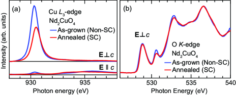
Figure 2(a) shows Cu -edge XAS spectra for and for as-grown and annealed Nd2CuO4 films. The spectra for were obtained by subtracting the contribution of from the spectra measured with polarization. The absorption intensity is proportional to the unoccupied density of states (DOS) of the specific element multiplied by transition matrix elements deGroot1990 , which depends on the initial- and final-state orbital symmetry as well as incident light polarization. Thus, XAS provides information about the element- and orbital-specific unoccupied DOS. With polarization , matrix element of the transition into the 3 orbital is three times larger than that into the 3 orbital, while the polarization allows only the transition into the 3 orbital (See Supplementary Information). The XAS spectra for show an intense peak at eV and its intensity decreases with annealing by 30 %, suggesting the reduction of unoccupied DOS near as reported for Ce-doped samples Flipse1990 ; Pellegrin1993 ; Fink1994 ; Steeneken2003 . In contrast, spectra for remains negligibly weak. This leads to a small ratio of the 3 weight to the 3 weight (4 % and 2 % for as-grown and annealed Nd2CuO4, respectively) in agreement with previous reports Pellegrin1993 ; Fink1994 . Therefore, the 3 orbitals are almost completely filled regardless of whether annealed or not, and additional electrons go to the 3 orbitals by annealing. On the other hand, the pre-edge peak ( 529 eV) in O -edge XAS measured with [Fig. 2(b)], which represents the transition from O 1 to in-plane O 2 orbitals hybridized with the upper Hubbard band, shows only a slight change (5 %) in contrast to Cu -edge XAS for . This agrees with the changes observed by Ce doping in the previous studies and suggests that the orbital character of the upper Hubbard band is dominated by 3 Flipse1990 ; Krol1990 ; Pellegrin1993 ; Fink1994 .
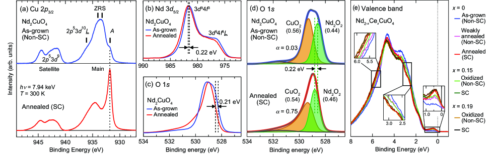
The effect of annealing is also remarkable in HAXPES spectra. Figure 3(a) shows the Cu 2 core-level HAXPES spectra of the as-grown and annealed Nd2CuO4 films. Upon photoemission from a core level, valence electrons are attracted to the core-hole site to screen its potential. Different types of core-hole screening result in various final states appearing as fine structures in the core-level photoemission spectra Veenendaal1993 . As has been discussed for the Cu 2 spectrum of insulating cuprates such as La2CuO4 Taguchi2005 ; Maiti2009 and Sr2CuO2Cl2 Boske_1997 ; Boske_1998 analyzed using multi-site cluster calculation, the peak at the highest binding energy ( = 940–947 eV) is the satellite due to the 23 final state with an unscreened core hole. In the main peak region ( = 930–939 eV), the highest binding energy peak corresponds to the 2 final state, where an electron is transferred from the neighboring oxygen atoms (local screening) leaving a hole in the oxygen ligand orbital , and the two peaks in the middle to the final state where an electron is transferred from oxygen in the neighboring CuO4 plaquettes thereby creating a Zhang-Rice singlet in the plaquettes (non-local screening). Apart from peak A at the lowest binding energy discussed below, the line shape of the main peak resembles those of the other insulating cuprates with two-dimensional CuO2 planes Boske_1998 .
Upon annealing, peak A is strongly enhanced and the entire line shape dramatically changes. The binding energies of the charge-transferred final state are determined by the energy levels of the electronic states from which the electron is transferred to screen the core-hole potential. Therefore, the enhancement of the lowest energy peak indicates the development of electronic states closest to the Fermi level () Taguchi2005 ; Panaccione2008 and is attributed to final states where the core hole is screened by conduction electrons. The observed changes in the present Cu 2 spectra therefore suggest that conduction electrons were introduced by annealing, consistent with the occurrence of superconductivity in the annealed Nd2CuO4.
The effect of annealing on the Nd and O core levels of Nd2CuO4 films is shown in Figs. 3(b)–(d). Upon annealing, the Nd 3 peak was shifted toward higher binding energy by 0.22 eV [Fig. 3(b)]. As for the O peak, a shift of similar amount (0.21 eV) was observed at the edge, but the spectral line shape is also modified: the full width at half maximum decreased from 1.44 eV to 1.16 eV and a long high binding energy tail emerges above eV [Fig. 3(c)]. Such changes have been overlooked in the doping and annealing dependence of the O photoemission spectra of Nd2-xCexCuO4 in previous studies Suzuki1990a ; Harima2001 . In order to disentangle this complicated spectral deformation, the O spectra have been analyzed as follows: The peak region of the O spectrum of the as-grown film is rather flat, implying unresolved two peaks with similar intensities. We attribute them to oxygen atoms in the Nd2O2 layers (O) and those in the CuO2 planes (O), which are contained in Nd2CuO4 with equal amount. We calculated the oxygen binding energies using a Wien2k package, and found that the O 1 level was located at a lower binding energy than the O 1 level Sup2 . Therefore, the O 1 spectra of the Nd2CuO4 films were fitted to a superposition of a Voigt function (for O) at lower binding energies and Mahan line shape convolved with a Voigt function (for O) at higher binding energies. The asymmetric Mahan line shape was assumed for O considering the core-hole screening by metallic electrons. Another Voigt function was added to the fitting function to reproduce a weak contamination component at eV. The fitting yielded O and O peaks with nearly the same area both for the as-grown and annealed films as shown in Fig. 3(d), consistent with the initial assumption that each O 1 spectrum consists of two components arising from O and O Sup3 . The present analysis thus enables us to identify the effect of annealing on the two O 1 core levels separately: The O peak was shifted by 0.22 eV toward higher binding energy, and the O peak became strongly asymmetric (represented by the increase of asymmetry parameter from 0.03 to 0.75). Since a finite DOS at leads to a peak asymmetry, the strong asymmetry of the O peak in the annealed Nd2CuO4 film is consistent with the dramatic enhancement of the electrical conductivity. Another remarkable point is that annealing shifted the O 1 peak by almost the same amount as the Nd 3 peak without appreciable changes in the line shapes.
The shift of the core-level binding energy is given by Hufner1995
| (1) |
where is the change in the chemical potential, is the change in the number of valence electrons, is a constant, is the change in the Madelung potential, and is the change in the extra-atomic screening of the core-hole potential by conduction electrons and/or dielectric polarization of surrounding media. Almost identical shifts observed for the Nd 3 and O 1 core levels indicate that is negligibly small because it would shift the core levels of the O2- anion and the Nd3+ cation in different ways. cannot be the main origin of the observed shifts, either, because the increase of conduction electrons by annealing would shift the core-level peaks toward lower binding energy, opposite to the experimental observation. Considering that the valences of Nd3+ and O2- are fixed (), we conclude that the observed shifts in Nd 3 and O 1 core levels of Nd2CuO4 are largely due to the chemical potential shift . The increase of the core-level binding energies by annealing indicates the increase of due to the addition of electrons.
Having identified the chemical-potential shift caused by annealing in Nd2CuO4, we compare the core-level structure of Nd2CuO4 with those of Ce-doped compounds. By Ce substitution, annealing, and oxidization, the Nd and Ce 3 spectra were shifted maintaining their shape. The line-shape changes in the Cu 2 and O 1 spectra were also consistent with the above scenario Sup4 . The chemical-potential shift defined as the average shift of the Nd 3 and O 1 core levels, is plotted in Fig, 4(a) against Ce concentration . For Nd2CuO4, the chemical potential is shifted upwards with annealing, reaching the level of Ce-doped and 0.19 superconductors when sufficiently annealed. The valence-band spectra shown in Fig. 3(e) and Supplementary Information are also almost identical among the three SC films with different Ce concentrations (, 0.15, and 0.19), indicating that the electronic structure and band filling are close to each other.
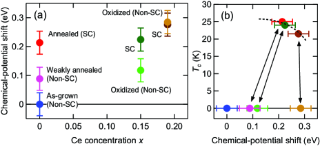
The large electron concentration for the annealed SC Nd2CuO4 film can be explained if oxygen atoms are removed not only from the apical site Radaelli1994 ; Schultz1996 but also from the regular sites (in the CuO2 plane and/or the Nd2O2 layer) Riou2004 ; Richard2004 , leading to the total oxygen content less than the stoichiometric one. On the other hand, upon oxidization of Nd2-xCexCuO4 (), chemical potential was shifted downwards as can be seen in Fig. 4(a). This may be because the SC film was already oxygen deficient and the vacancies were filled by oxidization. Consequently, the band filling of the T’-type cuprates is not determined by the Ce substitution alone but by the combined effect of Ce substitution and oxygen vacancies and, therefore, the phase diagram for this system should be made as a function of actual band filling, rather than as a function of Ce concentration. The oxidization process also introduced excess apical oxygen atoms, as suggested by the -axis elongation [Fig. 1(d)], and the film turned non-SC.
In Fig. 4(b), the ’s of Nd2-xCexCuO4 films are thus plotted against chemical-potential shift, which represents the electron concentration. The values are not solely determined by the electron concentration since films can be either SC or non-SC without a significant change in the electron concentration. The elongation of the -axis lattice parameter by oxidization is also rather small for the film (0.06 %) compared to that for film (0.12 %), indicating that only a tiny amount of apical oxygen atoms were incorporated. These results are consistent with previous studies where the amount of oxygen reduction decreases with increasing Ce concentrations Suzuki1990b ; Radaelli1994 ; Schultz1996 . The higher concentration of Ce4+ and the smaller -axis lattice parameter may make the Ce-overdoped samples more robust against oxygen non-stoichiometry induced by reduction annealing and oxidization. While oxygen vacancy at the regular sites increases the electron concentration, excess oxygen atoms at the apical site immediately destroy superconductivity. The electronic structure of the T’-type cuprates are thus dominated not only by Ce concentrations but also by oxygen non-stoichiometry.
In conclusion, we have performed HAXPES and XAS measurements on Nd2-xCexCuO4 ( = 0, 0.15, and 0.19) thin films with varying annealing atmosphere, and observed changes in the band-filling level among them. The electronic structure of SC Nd2CuO4 was found to be intimately linked to those of Ce-doped superconductors as the electrons were doped into the thin films by annealing probably through the creation of oxygen vacancies. Since the electron concentration and superconductivity of the T’-type cuprates are significantly affected by oxygen non-stoichiometry, the electronic structure should be discussed based on the actual electron concentration and oxygen occupancies rather than solely the Ce concentration.
Acknowledgements.
Fruitful discussion with K. Okada and G.R. Castro is gratefully acknowledged. Experiments were performed at SPring-8 (proposal Nos. 2015B1699, 2015B1793, 2015B7401, and 2016A1210). This work was supported by Grants-in-aid from the Japan Society of the Promotion of Science (JSPS) (grant Nos. 14J09200 and 15H02109). M.H. acknowledges support from the Advanced Leading Graduate Course for Photon Science (ALPS) and the JSPS Research Fellowship for Young Scientists.References
- (1) Y. Tokura, H. Takagi, and S. Uchida, Nature (London) 337, 345 (1989).
- (2) N. P. Armitage, P. Fournier, and R. L. Greene, Rev. Mod. Phys. 82, 2421 (2010).
- (3) P. G. Radaelli, J. D. Jorgensen, A. J. Schultz, J. L. Peng, and R. L. Greene, Phys. Rev. B 49, 15322 (1994).
- (4) A. J. Schultz, J. D. Jorgensen, J. L. Peng, and R. L. Greene, Phys. Rev. B 53, 5157 (1996).
- (5) G. Riou, P. Richard, S. Jandl, M. Poirier, P. Fournier, V. Nekvasil, S. N. Barilo, and L. A. Kurnevich, Phys. Rev. B 69, 024511 (2004).
- (6) P. Richard, G. Riou, I. Hetel, S. Jandl, M. Poirier, and P. Fournier, Phys. Rev. B 70, 064513 (2004).
- (7) H. J. Kang, P. Dai, B. J. Campbell, P. J. Chupas, S. Rosenkranz, P. L. Lee, Q. Huang, S. Li, S. Komiya, and Y. Ando, Nat. Mater. 6, 224 (2007).
- (8) P. Richard, M. Neupane, Y.-M. Xu, P. Fournier, S. Li, P. Dai, Z. Wang, and H. Ding, Phys. Rev. Lett. 99, 157002 (2007).
- (9) M. Horio, T. Adachi, Y. Mori, A. Takahashi, T. Yoshida, H. Suzuki, L. C. C. Ambolode, K. Okazaki, K. Ono, H. Kumigashira, H. Anzai, M. Arita, H. Namatame, M. Taniguchi, D. Ootsuki, K. Sawada, M. Takahashi, T. Mizokawa, Y. Koike, and A. Fujimori, Nat. Commun. 7, 10567 (2016).
- (10) X. Q. Xu, S. N. Mao, W. Jiang, J. L. Peng, and R. L. Greene, Phys. Rev. B 53, 871 (1996).
- (11) A. Tsukada, Y. Krockenberger, M. Noda, H. Yamamoto, D. Manske, L. Alff, and M. Naito, Solid State Commun. 133, 427 (2005).
- (12) A. Tsukada, M. Noda, H. Yamamoto, and M. Naito, Physica C 426-431, 459 (2005).
- (13) O. Matsumoto, A. Utsuki, A. Tsukada, H. Yamamoto, T. Manabe, and M. Naito, Physica C 469, 924 (2009).
- (14) Y. Krockenberger, H. Irie, O. Matsumoto, K. Yamagami, A. Tsukada, M. Naito, and H. Yamamoto, Sci. Rep. 3, 2235 (2013).
- (15) H. Das and T. Saha-Dasgupta, Phys. Rev. B 79, 134522 (2009).
- (16) C. Weber, K. Haule, and G. Kotliar, Nat. Phys. 6, 574 (2010).
- (17) C. Weber, K. Haule, and G. Kotliar, Phys. Rev. B 82, 125107 (2010).
- (18) P. K. Mang, O. P. Vajk, A. Arvanitaki, J. W. Lynn, and M. Greven, Phys. Rev. Lett. 93, 027002 (2004).
- (19) T. Arima, Y. Tokura, and S. Uchida, Phys. Rev. B 48, 6597 (1993).
- (20) D. Song, G. Han, W. Kyung, J. Seo, S. Cho, B. S. Kim, M. Arita, K. Shimada, H. Namatame, M. Taniguchi, Y. Yoshida, H. Eisaki, S. R. Park, and C. Kim, Phys. Rev. Lett. 118, 137001 (2017).
- (21) H. I. Wei, C. Adamo, E. A. Nowadnick, E. B. Lochocki, S. Chatterjee, J. P. Ruf, M. R. Beasley, D. G. Schlom, and K. M. Shen, Phys. Rev. Lett. 117, 147002 (2016).
- (22) See Supplementary Information for more detailed experimental setup, which includes Refs. [Wadati2013, ; Takata2005, ; Sacchi2005, ; NIST, ; Schroeder1996, ; Ruosi2014, ].
- (23) H. Wadati and A. Fujimori, J. Electron Spectrosc. Relat. Phenom. 190, 222 (2013).
- (24) Y. Takata, M. Yabashi, K. Tamasaku, Y. Nishino, D. Miwa, T. Ishikawa, E. Ikenaga, K. Horiba, S. Shin, M. Arita, K. Shimada, H. Namatame, M. Taniguchi, H. Nohira, T. Hattori, S. Södergren, B. Wannberg, and K. Kobayashi, Nucl. Instr. Methods A 547, 50 (2005).
- (25) M. Sacchi, F. Offi, P. Torelli, A. Fondacaro, C. Spezzani, M. Cautero, G. Cautero, S. Huotari, M. Grioni, R. Delaunay, M. Fabrizioli, G. Vankó, G. Monaco, G. Paolicelli, G. Stefani, and G. Panaccione, Phys. Rev. B 71, 155117 (2005).
- (26) NIST Electron Inelastic-Mean-Free-Path database, Version 1.1, National Institute of Standard and Technology, U.S., 2000.
- (27) S. L. Schroeder, Solid State Commun. 98, 405 (1996).
- (28) A. Ruosi, C. Raisch, A. Verna, R. Werner, B. A. Davidson, J. Fujii, R. Kleiner, and D. Koelle, Phys. Rev. B 90, 125120 (2014).
- (29) F. M. F. de Groot, J. C. Fuggle, B. T. Thole, and G. A. Sawatzky, Phys. Rev. B 42, 5459 (1990).
- (30) C. F. J. Flipse, G. van der Laan, A. L. Johnson, and K. Kadowaki, Phys. Rev. B 42, 1997 (1990).
- (31) E. Pellegrin, N. Nücker, J. Fink, S. L. Molodtsov, A. Gutiérrez, E. Navas, O. Strebel, Z. Hu, M. Domke, G. Kaindl, S. Uchida, Y. Nakamura, J. Markl, M. Klauda, G. Saemann-Ischenko, A. Krol, J. L. Peng, Z. Y. Li, and R. L. Greene, Phys. Rev. B 47, 3354 (1993).
- (32) J. Fink, N. Nücker, E. Pellegrin, H. Romberg, M. Alexander, and M. Knupfer, J. Electron Spectrosc. Relat. Phenom. 66, 395 (1994).
- (33) P. G. Steeneken, L. H. Tjeng, G. A. Sawatzky, A. Tanaka, O. Tjernberg, G. Ghiringhelli, N. B. Brookes, A. A. Nugroho, and A. A. Menovsky, Phys. Rev. Lett. 90, 247005 (2003).
- (34) A. Krol, C. S. Lin, Z. H. Ming, C. J. Sher, Y. H. Kao, C. L. Lin, S. L. Qiu, J. Chen, J. M. Tranquada, M. Strongin, G. C. Smith, Y. K. Tao, R. L. Meng, P. H. Hor, C. W. Chu, G. Cao, and J. E. Crow, Phys. Rev. B 42, 4763 (1990).
- (35) M. A. van Veenendaal and G. A. Sawatzky, Phys. Rev. Lett. 70, 2459 (1993).
- (36) M. Taguchi, A. Chainani, K. Horiba, Y. Takata, M. Yabashi, K. Tamasaku, Y. Nishino, D. Miwa, T. Ishikawa, T. Takeuchi, K. Yamamoto, M. Matsunami, S. Shin, T. Yokoya, E. Ikenaga, K. Kobayashi, T. Mochiku, K. Hirata, J. Hori, K. Ishii, F. Nakamura, and T. Suzuki, Phys. Rev. Lett. 95, 177002 (2005).
- (37) K. Maiti, J. Fink, S. de Jong, M. Gorgoi, C. Lin, M. Raichle, V. Hinkov, M. Lambacher, A. Erb, and M. S. Golden, Phys. Rev. B 80, 165132 (2009).
- (38) T. Böske, O. Knauff, R. Neudert, M. Kielwein, M. Knupfer, M. S. Golden, J. Fink, H. Eisaki, S. Uchida, K. Okada, and A. Kotani, Phys. Rev. B 56, 3438 (1997).
- (39) T. Böske, K. Maiti, O. Knauff, K. Ruck, M. S. Golden, G. Krabbes, J. Fink, T. Osafune, N. Motoyama, H. Eisaki, and S. Uchida, Phys. Rev. B 57, 138 (1998).
- (40) G. Panaccione, F. Offi, P. Torelli, G. Vanko, O. Tjernberg, P. Lacovig, A. Guarino, A. Fondacaro, A. Nigro, M. Sacchi, N. B. Brookes, and G. Monaco, Phys. Rev. B 77, 125133 (2008).
- (41) T. Suzuki, M. Nagoshi, Y. Fukuda, K. Oh-ishi, Y. Syono, and M. Tachiki, Phys. Rev. B 42, 4263 (1990).
- (42) N. Harima, J. Matsuno, A. Fujimori, Y. Onose, Y. Taguchi, and Y. Tokura, Phys. Rev. B 64, 220507 (2001).
- (43) See Supplementary Information for details of calculation, which includes Ref. [Slater1971, ].
- (44) J. C. Slater, Int. J. Quantum. Chem. S4, 3 (1971).
- (45) See Supplementary Information for more details about the fitting procedure, which includes Refs. [Ikeda2009, ; Sankari2003, ; Citrin1974, ].
- (46) M. Ikeda, T. Yoshida, A. Fujimori, M. Kubota, K. Ono, H. Das, T. Saha-Dasgupta, K. Unozawa, Y. Kaga, T. Sasagawa, and H. Takagi, Phys. Rev. B 80, 014510 (2009).
- (47) R. Sankari, M. Ehara, H. Nakatsuji, Y. Senba, K. Hosokawa, H. Yoshida, A. D. Fanis, Y. Tamenori, S. Aksela, and K. Ueda, Chem. Phys. Lett. 380, 647 (2003).
- (48) P. H. Citrin, P. Eisenberger, and D. R. Hamann, Phys. Rev. Lett. 33, 965 (1974).
- (49) S. Hüfner, Photoelectron Spectroscopy (Springer-Verlag, Berlin, 1995), Chap. 2, p. 35.
- (50) See Supplementary Information for individual spectra, which includes Ref. [Kotani1974, ].
- (51) A. Kotani and Y. Toyozawa, J. Phys. Soc. Jpn. 37, 912 (1974).
- (52) K. Suzuki, K. Kishio, T. Hasegawa, and K. Kitazawa, Physica C 166, 357 (1990).