Large gap quantum spin Hall insulator, massless Dirac fermions and bilayer graphene analogue in InAs/Ga(In)Sb heterostructures
Abstract
The quantum spin Hall insulator (QSHI) state has been demonstrated in two semiconductor systems – HgTe/CdTe quantum wells (QWs) and InAs/GaSb QW bilayers. Unlike the HgTe/CdTe QWs, the inverted band gap in InAs/GaSb QW bilayers does not open at the point of the Brillouin zone, preventing the realization of massless Dirac fermions. Here, we propose a new class of semiconductor systems based on InAs/Ga(In)Sb multilayers, hosting a QSHI state, a graphene-like phase and a bilayer graphene analogue, depending on their layer thicknesses and geometry. The QSHI gap in the novel structures can reach up to 60 meV for realistic design and parameters. This value is twice as high as the thermal energy at room temperature and significantly extends the application potential of III-V semiconductor-based topological devices.
pacs:
73.21.Fg, 73.43.Lp, 73.61.Ey, 75.30.Ds, 75.70.Tj, 76.60.-kIntroduction.–Quantum spin Hall insulators (QSHIs), also known as two-dimensional (2D) topological insulators (TIs), are characterized by an insulating bulk and spin-polarized gapless helical states at the sample edges Hasan and Kane (2010); Qi and Zhang (2011); Bernevig et al. (2006). Those edge states are protected from backscattering by time reversal symmetry, promoting dissipationless electric currents. QSHIs also offer realizations of numerous non-trivial properties, such as unusual magnetoelectric effects Qi et al. (2008) and Majorana fermion bound states, arising at the interface with superconductors Fu and Kane (2008); Nilsson et al. (2008). Experimental demonstrations of QSHI are so far limited to two semiconductor systems – HgTe/CdTe quantum wells (QWs) König et al. (2007) and InAs/GaSb bilayers Liu et al. (2008); Knez et al. (2011).
The central feature of the HgTe/CdTe QWs is the possibility of band inversion by changing of QW width . QWs wider than a critical thickness have inverted band structure Gerchikov and Subashiev (1990), at which the lowest electron-like subband (E1) lies lower in energy than the top heavy-hole-like subband (H1). The band inversion drives the system into the QSHI state Bernevig et al. (2006), with gapless edge channels. At , the E1 subband lies above H1 level and the systems features the band insulator (BI) state. At the critical thickness, the HgTe QWs possess a single-valley spin-degenerate Dirac cone at the point of the Brillouin zone Büttner et al. (2011). The maximum inverted band gap in HgTe/CdTe QWs grown on CdTe does not exceed 16 meV. Recently, P. Leubner et al. have reported realization of QSHI with a band gap up to 55 meV in compressively strained HgTe QWs Leubner et al. (2016).
The InAs/GaSb bilayers consist of two layers of InAs and GaSb confined between AlSb barriers. The valence band edge of GaSb is 0.15 eV higher than the conduction band edge of the InAs layer, thus, depending on the layer thicknesses, a band inversion arises. Since the InAs/GaSb bilayers do not have inversion symmetry in the growth direction, the crossing of E1 and H1 subbands arises away from the point of the Brillouin zone Murakami et al. (2007). Therefore, this band gap vanishing does not reveal a Dirac cone due to the mixing between E1 and H1 levels at non-zero quasimomentum , which opens a hybridization gap and drives the system into the QSHI regime. The typical band gap values in the inverted InAs/GaSb bilayers are of several meV Liu et al. (2008).
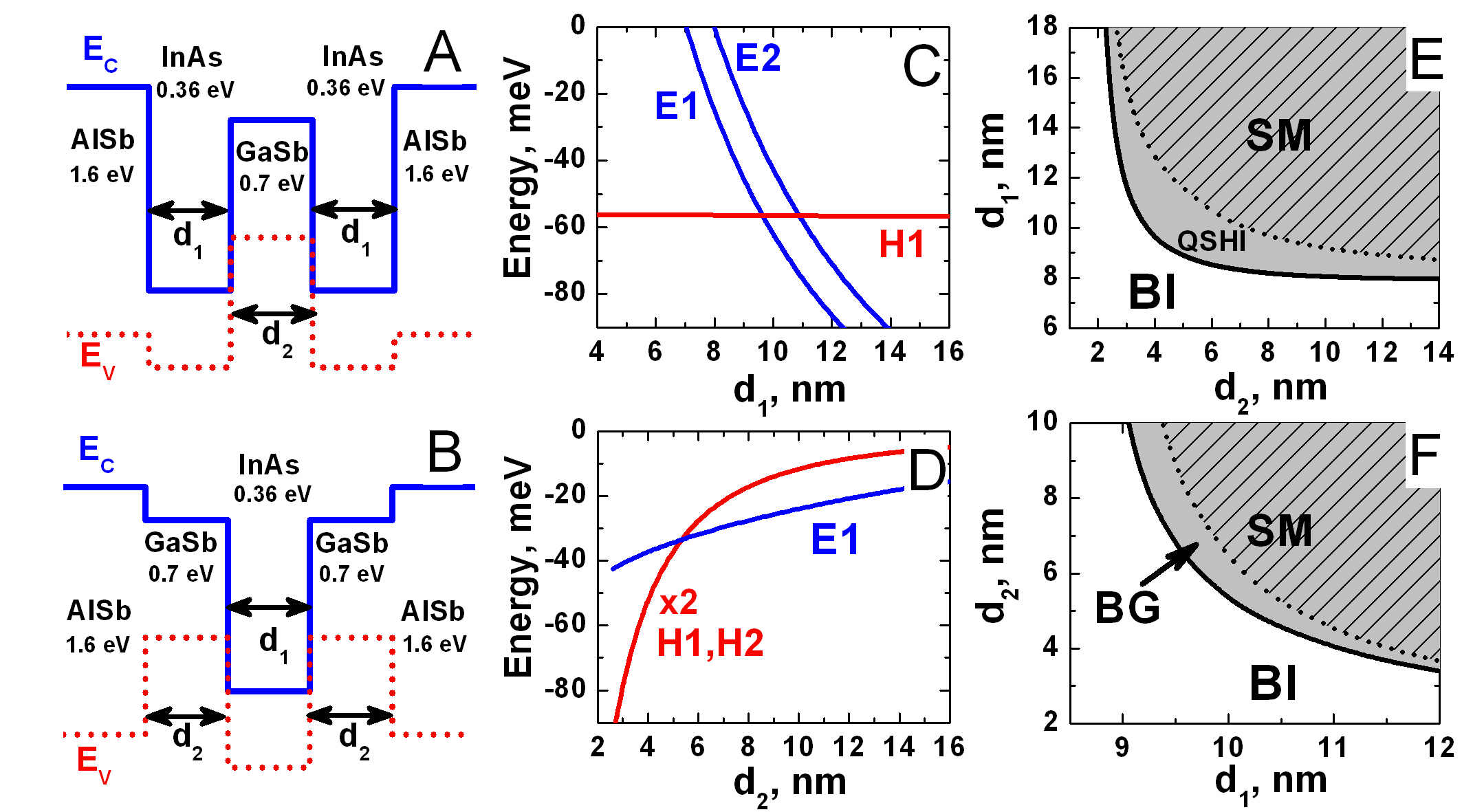
In this work, we introduce a new class of multi-layered InAs/Ga(In)Sb QWs, which differ from the bilayers by the band crossing at the point of the Brillouin zone. To eliminate the inversion asymmetry in the growth direction, we attach an additional InAs or GaSb layer to the InAs/GaSb bilayer. Further, we call the three-layer InAs/GaSb QW as InAs-designed QW (Fig. 1A) or GaSb-designed QW (Fig. 1B) if it contains two layers of InAs or GaSb, respectively.
Phase transitions in three-layer InAs/GaSb QWs.–
To investigate the band ordering, we have performed band structure calculations on the basis of the full 8-band Kane model Krishtopenko et al. (2016a) with material parameters taken from Vurgaftman et al. (2001). Figure 1C shows positions of electron-like and hole-like subbands at zero quasimomentum in the InAs-designed QW as a function of InAs-layer thickness . The QWs are supposed to be grown on GaSb buffer along (001) crystallographic direction.
As the electron-like subbands are localized in the InAs layers, while the hole-like subbands are localized in the GaSb layers, the InAs-designed QW can be contingently considered as ”double QW for electrons” with GaSb middle barrier ( nm), which also plays a role of ”QW for holes”. In this case, the electron-like levels E1 and E2 are connected with even-odd state splitting, arising from the tunnel-coupled ”QWs for electrons”. If InAs layers are thin (, is a function of ), the E1 and E2 subband lie above the position of valence band edge in bulk GaSb, and the three-layer QW is in normal regime. For , the E1 subband lies below the H1 level and the QW has an inverted band ordering.

In contrast, the GaSb-designed QW contains two tunnel-coupled ”QWs for holes” with InAs layer as ”middle barrier”. The InAs layer at nm is not transparent for the particles from the hole-like subbands due to their large effective mass. Therefore, the hole-like subbands are degenerated at . The mixing between heavy-hole-like and electron-like states at non-zero leads to the splitting between H1 and H2 subbands. Figure 1D shows positions of E1, H1 and H2 subbands at in GaSb-designed QW with nm as a function of . If GaSb layers are thin enough so that (where depends on ), the E1 level lies below H1 and H2 subbands, and the band structure is inverted. For , the QW has direct band structure.
For both types of three-layer structures, we have explored the phase diagrams, shown in Fig. 1E and 1F. In each diagram, the solid curve, describing the crossing between E1 and H1 subbands, divides the – plane into white region, corresponding to the BI phase with direct band ordering, and grey region with inverted band structure.
The grey region for InAs-designed QWs is splitted into open and striped areas, corresponding to QSHI and semimetal (SM) phase, respectively. The SM phase is characterized by a vanishing indirect band gap, when the side maxima of the valence subband exceed in energy the conduction subband bottom. This phase is also present in wide HgTe QWs Kvon et al. (2008, 2011). The typical band dispersions for each phase are presented in Q (20).
The band inversion in GaSb-designed QWs drives the BI state into a metal phase with a band structure consisting of two isotropic parabolas, formed by conduction subband H1 and valence subband H2 touching at . Such band structure is very similar to the one of natural bilayer graphene (BG) Ohta et al. (2006). The reasons for naming this metal phase as a BG phase will be discussed later. Further increasing of and transforms a BG phase into a metal phase, which, in addition to the band touching at , is also characterized by non-local overlapping of the valence subband with the loop of side minima in the conduction subband. This unconventional SM phase is presented by grey-striped area in Fig. 1F. Typical band dispersion for each phase is provided in Q (20).
To describe quantum phase transition, we derive effective 2D Hamiltonian for both types of the QWs. In addition to E1 and H1 levels, we should also take into account adjacent E2 subband for the InAs-designed QWs and H2 subband for the GaSb-designed QWs. Following the procedure described in Bernevig et al. (2006); Krishtopenko et al. (2016b), 2D Hamiltonian for the InAs-designed QWs in the basis E1,+, H1,+, E2,-, E1,-, H1,-, E2,+ has the form:
| (1) |
where asterisk stands for complex conjugation, and are momentum components in the plane, and is written as
| (2) |
in which , and . Here, , , , , , , , are structure parameters, which depend on and and . The sign of mass parameter defines inversion of the E1 and H1 levels. Additional parameter describes the gap between the E1 and E2 subbands at . Since we have kept the inversion symmetry and axial symmetry around the growth direction, has a block-diagonal form.
In the basis E1,+, H1,+, H2,-, E1,-, H1,-, H2,+, 2D Hamiltonian for the GaSb-designed QWs has the form of (1) but with defined as
| (3) |
where . Here, the terms and have the same form as in Eq. (2), depends only on thickness of InAs and GaSb layers. Parameters for both 2D Hamiltonians and comparison with band structure calculations on the basic of the 8-band Kane model are given in Q (20). At , both Hamiltonians are reduced to Hamiltonian of massless Dirac fermions with Fermi velocity , defined by parameter . The values of in three-layer InAs/GaSb QWs are varied from m/s to m/s depending on the layer thicknesses and buffer material Q (20).

QSHI in InAs-designed QWs.–QSHI state in the InAs-designed QWs occurs in the inverted regime, in which the massless helical states are confined on the sample edge. The latter can be shown by solving the eigenvalue problem for with and open boundary condition along one of the directions Q (20).
In the bilayers, the inverted gap opens away from the point of the Brillouin zone due to the mixing of E1 and H1 levels. In the case of three-layer InAs/GaSb QWs, the inverted band gap arises at due to quantum confinement, while the E1-H1 mixing vanishes at . Since the confinement effect is much stronger then the E1-H1 interaction at non-zero , we expect higher values of the inverted band gap in the novel structures than in InAs/GaSb bilayers.
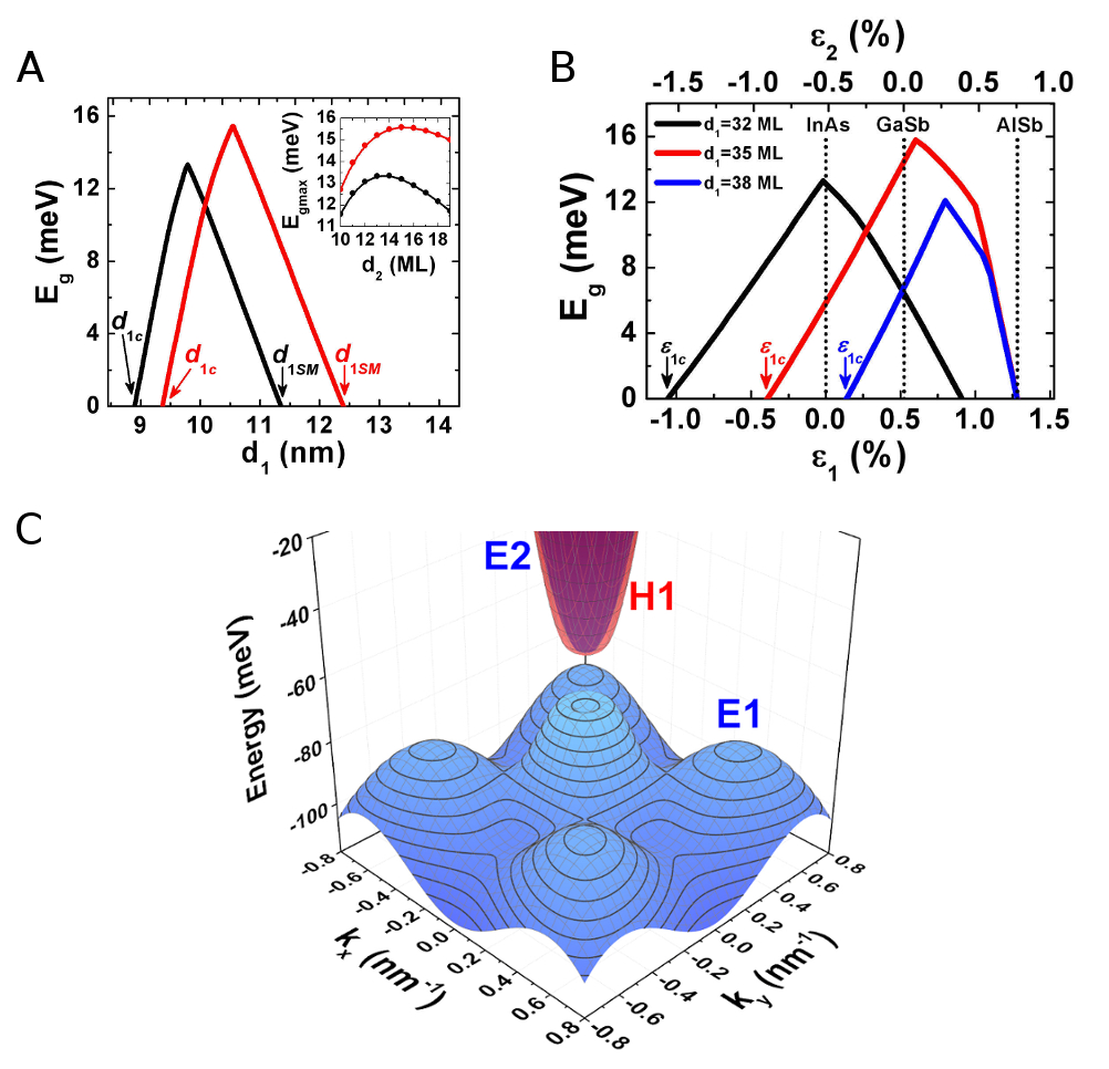
Figure 2A shows the band gap in QSHI state as a function of for monolayers (ML). Here, 1 ML in the given QW layer corresponds to a half of a lattice constant in the bulk material. It is seen that, at , increasing of induces increasing of the inverted band gap, which occurs between H1 and E1 levels. When the band gap becomes close to (see Fig. 2C), the system transforms into indirect-band-gap QSHI, in which H1 level lies above E2 subband. Further increasing of decreases the indirect-band-gap between and subbands until it vanishes at . The latter causes a transition into SM phase. The values of and also depend on the strain in InAs and GaSb layers, which can be varied by changing the buffer material.
Figure 2B provides the inverted band gap as a function of strain in InAs layers and GaSb layer . The values of and are connected via the lattice constant of the buffer material. It is seen that by tuning the strain one can induce transitions between BI, QSHI and SM phases. The value of , corresponding to the crossing between E1 and H1 level, is marked by vertical arrow and defined as . It is seen that by adjusting the strain and the values of and , one can realized a QSHI with a band gap up to 16 meV. For instance, the QW with ML and ML grown on GaSb buffer has a QSHI state with a gap close to the maximum value (see Fig. 2C). The band gap of 16 meV is in several times greater than the band gap in inverted InAs/GaSb bilayers Liu et al. (2008). It is interesting that the QWs grown on AlSb buffer do not feature a QSHI state. In this case, the band inversion at is accompanied by nonlocal overlapping between conduction and valence bands.
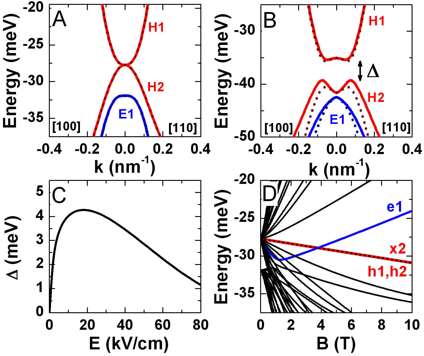
BG phase in GaSb-designed QWs.–The band structure in this phase mimics the structure of natural BG (see Fig. 3A). In natural BG, a band gap can be opened by breaking of inversion symmetry between layers, for instance, by electric field perpendicular to the sample plane. The GaSb-designed QW also holds this property.
Fig. 3B shows the band structure for the BG phase in electric field of 5 kV/cm. The dispersion curves are very similar to the band structure of natural BG in electric field Ohta et al. (2006). However, the strong spin-orbit interaction in the GaSb-designed QWs removes the spin degeneracy at non-zero due to Rashba effect Rashba (1960). Fig. 3C shows the band gap as a function of electric field. It is seen that the band gap is electrically-tunable, as it is in natural BG, although its dependence on electric field in the GaSb-designed QWs has non-monotonic behaviour.

Another characteristic of natural BG is the unconventional quantum Hall effect Novoselov et al. (2006). For natural BG, plateaus in the Hall conductivity , occur at integer multiples of , where the level degeneracy arises from the spin and valley degrees of freedom. Deviation from the conventional case occurs in the vicinity of the charge neutrality point, where there is a step in of height , arising from the eight-fold degeneracy of the zero-energy LL.
In the GaSb-designed QWs, a specific zero-mode LL with degeneracy two times higher than other LLs also arises. This zero-mode LL is presented in Fig. 3D by the bold red curve (the h1 and h2 levels). The doubled degeneracy of such LL requires two times more carriers to fill it, so the transition between the corresponding plateaus should be twice as wide in density as others, and the step between the plateaus are expected to be instead of . As inversion asymmetry in the GaSb-designed QWs splits the zero-mode LLs, removing the double degeneracy order, we anticipate the recovery of the equidistant sequence of the plateaus such as for gate-biased natural BG Castro et al. (2007).
In the GaSb-designed QWs, there is another specific LL, which has a pure electron-like character at high magnetic field. The crossing of such level, denoted as e1 in Fig. 3D, with the zero mode LL, arising at critical magnetic field T, corresponds to the transition from inverted into normal band ordering König et al. (2007).
The main difference between natural BG and the BG phase is that the electrons in the GaSb-designed QWs are not chiral particles although they mimic some characteristics of natural BG. Moreover, one can show Q (20) that the BG phase is a straight realization of the recently predicted state of matter, in which the gapless bulk states and spin-polarized edge channels coexist Baum et al. (2015). Previously, the BG phase was also predicted for two tunnel-coupled HgTe QWs Ohta et al. (2006).

Large gap QSHI in InAs-designed QWs.–We have demonstrated that InAs/GaSb/InAs and HgTe/CdTe QWs share the same phases. Now, we address the question if the inverted band gap in the three-layer QWs can be enhanced up to 55 meV, known for the compressively strained HgTe QWs Leubner et al. (2016). To increase the band gap, we replace the middle GaSb layer by a GaInSb alloy Smith and Mailhiot (1987). Recently, this idea has been applied to the InAs/GaInSb QW bilayers Akiho et al. (2016); Du et al. (2017), in which the band gap is increased up to 20 meV for realistic indium content.
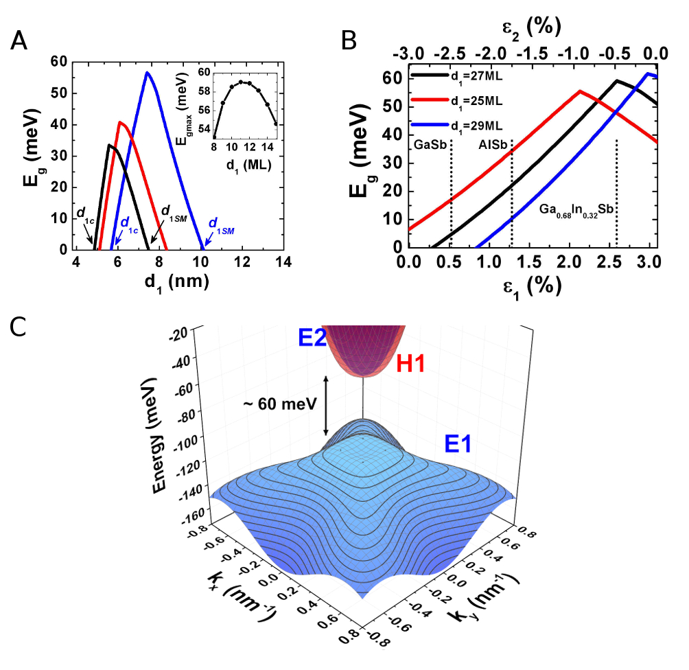
Figure 4A shows the inverted band gap in the three-layer InAs/Ga0.6In0.4Sb QW grown on various buffers as a function of at ML. The inset shows the maximum gap at given value of in the QW grown on Ga0.68In0.32Sb buffer. Figure 4B provides the inverted band gap for the InAs/Ga0.6In0.4Sb QWs with different values of and ML as a function of strain in InAs layers and Ga0.6In0.4Sb layer . Figure 4B demonstrates that by adjusting the strain, and , one can obtain a QSHI with a band gap up to 60 meV. Indeed, the InAs/Ga0.6In0.4Sb QW with ML and ML grown on Ga0.68In0.32Sb buffer (see Fig. 4C) features the inverted band gap of about 60 meV. We note that the maximum band gap in QSHI state is achieved only symmetrical InAs/GaInSb/InAs QWs Q (20).
Recent progress in the MBE technology of InAs/GaInSb structures Patrashin et al. (2011, 2017) allows pseudomorphic growth of 40-period strained InAs/Ga0.6In0.4Sb SLs with good structural and surface quality. As InAs/Ga1-xInxSb QWs do not require so large critical layer thickness, the pseudomorphic growth of InAs/Ga1-xInxSb QW structures may be possible even at . Therefore, an inverted band gap of more than 60 meV is expected in these QWs.
Finally, we stress an important advantage of three-layer InAs/GaInSb QWs as compared with HgTe/CdTe QWs. The inverted band gap in HgTe/CdTe QWs dramatically decreases with temperature Wiedmann et al. (2015); Teppe et al. (2016); Marcinkiewicz et al. (2017). Therefore, a QSHI with the large gap in compressively strained HgTe/CdHgTe QWs is available at low temperatures only. Since temperature does not affect the ordering of the and bands in bulk InSb, InAs, GaSb semiconductors, we expect a weaker temperature effect on the band gap in the inverted InAs/GaInSb QWs.
Acknowledgements.
This work was supported by the Occitanie region via the ”Gepeto Terahertz platform” and the ARPE project ”Terasens”, by the CNRS through the Emergence project 2016, and through the LIA ”TeraMIR” project, by Montpellier University through the ”Terahertz Occitanie Platform (TOP)” and by Russian Ministry of Education and Science (MK-1136.2017.2). Theoretical studies of the edge states were performed in the framework of project 16-12-10317 provided by Russian Science Foundation. Investigation of in multi-layered InAs/GaInSb QWs was supported by project 17-72-10158 from Russian Science Foundation.
References
- Hasan and Kane (2010) M. Z. Hasan and C. L. Kane, Rev. Mod. Phys. 82, 3045 (2010).
- Qi and Zhang (2011) X.-L. Qi and S.-C. Zhang, Rev. Mod. Phys. 83, 1057 (2011).
- Bernevig et al. (2006) B. A. Bernevig, T. L. Hughes, and S.-C. Zhang, Science 314, 1757 (2006).
- Qi et al. (2008) X.-L. Qi, T. L. Hughes, and S.-C. Zhang, Phys. Rev. B 78, 195424 (2008).
- Fu and Kane (2008) L. Fu and C. L. Kane, Phys. Rev. Lett. 100, 096407 (2008).
- Nilsson et al. (2008) J. Nilsson, A. R. Akhmerov, and C. W. J. Beenakker, Phys. Rev. Lett. 101, 120403 (2008).
- König et al. (2007) M. König, S. Wiedmann, C. Brüne, A. Roth, H. Buhmann, L. W. Molenkamp, X.-L. Qi, and S.-C. Zhang, Science 318, 766 (2007).
- Liu et al. (2008) C. Liu, T. L. Hughes, X.-L. Qi, K. Wang, and S.-C. Zhang, Phys. Rev. Lett. 100, 236601 (2008).
- Knez et al. (2011) I. Knez, R.-R. Du, and G. Sullivan, Phys. Rev. Lett. 107, 136603 (2011).
- Gerchikov and Subashiev (1990) L. G. Gerchikov and A. V. Subashiev, Phys. Status Solidi B 160, 443 (1990).
- Büttner et al. (2011) B. Büttner, C. Liu, G. Tkachov, E. Novik, C. Brüne, H. Buhmann, E. Hankiewicz, P. Recher, B. Trauzettel, S. Zhang, and L. Molenkamp, Nat. Phys. 7, 418 (2011).
- Leubner et al. (2016) P. Leubner, L. Lunczer, C. Brüne, H. Buhmann, and L. W. Molenkamp, Phys. Rev. Lett. 117, 086403 (2016).
- Murakami et al. (2007) S. Murakami, S. Iso, Y. Avishai, M. Onoda, and N. Nagaosa, Phys. Rev. B 76, 205304 (2007).
- Krishtopenko et al. (2016a) S. S. Krishtopenko, I. Yahniuk, D. B. But, V. I. Gavrilenko, W. Knap, and F. Teppe, Phys. Rev. B 94, 245402 (2016a).
- Vurgaftman et al. (2001) I. Vurgaftman, J. R. Meyer, and L. R. Ram-Mohan, J. Appl. Phys. 89, 5815 (2001).
- Kvon et al. (2008) Z. Kvon, E. Olshanetsky, D. Kozlov, N. Mikhailov, and S. Dvoretskii, JETP Lett. 87, 502 (2008).
- Kvon et al. (2011) Z. D. Kvon, E. B. Olshanetsky, E. G. Novik, D. A. Kozlov, N. N. Mikhailov, I. O. Parm, and S. A. Dvoretsky, Phys. Rev. B 83, 193304 (2011).
- Q (20) See Supplementary Materials, which also include Refs. [33,34] .
- Ohta et al. (2006) T. Ohta, A. Bostwick, T. Seyller, K. Horn, and E. Rotenberg, Science 313, 951 (2006).
- Krishtopenko et al. (2016b) S. S. Krishtopenko, W. Knap, and F. Teppe, Sci. Rep. 6, 30755 (2016b).
- Rashba (1960) E. Rashba, Sov. Phys. Solid. State 2, 1109 (1960).
- Novoselov et al. (2006) K. S. Novoselov, E. McCann, S. V. Morozov, V. I. Fal’ko, M. I. Katsnelson, U. Zeitler, D. Jiang, F. Schedin, and A. K. Geim, Nat. Phys. 2, 177 (2006).
- Castro et al. (2007) E. V. Castro, K. S. Novoselov, S. V. Morozov, N. M. R. Peres, J. M. B. L. dos Santos, J. Nilsson, F. Guinea, A. K. Geim, and A. H. C. Neto, Phys. Rev. Lett. 99, 216802 (2007).
- Baum et al. (2015) Y. Baum, T. Posske, I. C. Fulga, B. Trauzettel, and A. Stern, Phys. Rev. Lett. 114, 136801 (2015).
- Smith and Mailhiot (1987) D. L. Smith and C. Mailhiot, J. Appl. Phys. 62, 2545 (1987).
- Akiho et al. (2016) T. Akiho, F. Couedo, H. Irie, K. Suzuki, K. Onomitsu, and K. Muraki, Appl. Phys. Lett. 109, 192105 (2016).
- Du et al. (2017) L. Du, T. Li, W. Lou, X. Wu, X. Liu, Z. Han, C. Zhang, G. Sullivan, A. Ikhlassi, K. Chang, and R.-R. Du, Phys. Rev. Lett. 119, 056803 (2017).
- Patrashin et al. (2011) M. Patrashin, I. Hosako, and K. Akahane, Proc. SPIE 8188, 81880G (2011).
- Patrashin et al. (2017) M. Patrashin, K. Akahane, N. Sekine, and I. Hosako, J. Cryst. Growth (2017), 10.1016/j.jcrysgro.2017.02.030.
- Wiedmann et al. (2015) S. Wiedmann, A. Jost, C. Thienel, C. Brüne, P. Leubner, H. Buhmann, L. W. Molenkamp, J. C. Maan, and U. Zeitler, Phys. Rev. B 91, 205311 (2015).
- Teppe et al. (2016) F. Teppe, M. Marcinkiewicz, S. S. Krishtopenko, S. Ruffenach, C. Consejo, A. M. Kadykov, W. Desrat, D. But, W. Knap, J. Ludwig, S. Moon, D. Smirnov, M. Orlita, Z. Jiang, S. V. Morozov, V. Gavrilenko, N. N. Mikhailov, and S. A. Dvoretskii, Nat. Commun. 7, 12576 (2016).
- Marcinkiewicz et al. (2017) M. Marcinkiewicz, S. Ruffenach, S. S. Krishtopenko, A. M. Kadykov, C. Consejo, D. B. But, W. Desrat, W. Knap, J. Torres, A. V. Ikonnikov, K. E. Spirin, S. V. Morozov, V. I. Gavrilenko, N. N. Mikhailov, S. A. Dvoretskii, and F. Teppe, Phys. Rev. B 96, 035405 (2017).
- Tkachov and Hankiewicz (2010) G. Tkachov and E. M. Hankiewicz, Phys. Rev. Lett. 104, 166803 (2010).
- Zhang et al. (2014) S.-B. Zhang, Y.-Y. Zhang, and S.-Q. Shen, Phys. Rev. B 90, 115305 (2014).