Topology driven g-factor tuning in type-II quantum dots
Abstract
We investigate how the voltage control of the exciton lateral dipole moment induces a transition from singly to doubly connected topology in type-II InAs/GaAsSb quantum dots. The latter causes visible Aharonov-Bohm oscillations and a change of the exciton -factor which are modulated by the applied bias. The results are explained in the frame of realistic and effective Hamiltonian models and could open a venue for new spin quantum memories beyond the InAs/GaAs realm.
pacs:
I Introduction
III-V semiconductor quantum dots (QDs) are a fundamental resource for quantum optical information technologies, from integrated quantum light sources to quantum optical processors.Michler (2017) Within this broad field, most knowledge arises from the InAs/GaAs system, with many other compounds being still relatively unexplored. III-Sb QDs and rings are a good example. They can be grown by several epitaxial methods and can strongly emit in all the relevant telecom bands, yet, III-Sb infrared quantum light sources are to be developed. III-Sb compounds also have the largest -factor and spin-orbit coupling (SOC) constant of all semiconductors but, with the exception of InSb nanowires, Nadj-Perge et al. (2012) this advantage has yet to be exploited in spin based quantum information technologies. One advantage of III-V-based quantum nanostructures is that optical initialization and read-out can be done in a few nanoseconds using, for instance, the singly charged exciton lambda system with electrons Atatüre et al. (2006) or holes Brunner et al. (2009). Using the hole brings the additional benefit of its p-orbital character, meaning that the overlap between the atomic orbitals and the nucleus is significantly smaller than for the s-like electrons, diminishing the decoherence caused by the hyperfine interaction. Brunner et al. (2009); Vidal et al. (2016)
For quantum information processing in the solid state, the possibility to modify the -factor through an external bias is its most outstanding resource. Nowack et al. (2007) Thanks to spin orbit coupling terms in the Hamiltonian, the application of an electric field can modify the -factor magnitude and sign through changes in the orbital part of the QD wavefunctions Pingenot et al. (2008); Andlauer and Vogl (2009); Pingenot et al. (2011). A similar effect can be obtained changing the elastic strain around the QD. Tholen et al. (2016) Since the -factor and wavefunctions are anisotropic, the observed modulation is different in Faraday Klotz et al. (2010); Jovanov et al. (2011); Ares et al. (2013); Corfdir et al. (2014) and Voigt Godden et al. (2012) configurations. With InAs/GaAs QDs, external bias in the range of tens of kV cm-1 is necessary and, to prevent electron tunneling out of the QD, the introduction of blocking barriers is advisable. Bennett et al. (2013); Prechtel et al. (2015) Alternately, one could use semiconductor nanostructures with larger spin orbit coupling constants to produce larger modulations at lower bias.
Meanwhile, quantum nanostructures with a ring-shaped topology for electrons, holes or both and type-I or type-II confinement have been the object of intense theoretical and experimental research. Fomin (2014); Lorke et al. (2000); Fuhrer et al. (2001); Ribeiro et al. (2004); Dias da Silva et al. (2005); Kleemans et al. (2007); Kuskovsky et al. (2007); Sellers et al. (2008); Teodoro et al. (2010); Miyamoto et al. (2010); Kim et al. (2016). When two particles travel around these quantum rings (QR) circumventing a magnetic flux, the Aharonov-Bohm (AB) effect changes the relative phase factor of their wave functions. Aharonov and Bohm (1959) The optical Aharonov-Bohm effect (OABE) can be detected at optical frequencies through the relative changes in the electron and hole orbital angular momenta. At zero magnetic field, electron-hole exchange interaction typically leads to a dark ground state doublet split by few hundred eV from the bright exciton doublet. With increasing applied magnetic field, higher energy states with non-zero orbital angular momentum cross this quadruplet becoming the new ground state of the system. These states are hence optically forbidden and must produce a fade-out of the emitted intensity. Govorov et al. (2002) In actual samples such a reduction on the emitted light is not observed because of the reduced symmetry of the system, i.e. the orbital angular momentum is not a good quantum number any longer. As a consequence, oscillations in energy and intensity are observed instead of a quench. Govorov et al. (2002) The evolution of charged excitons becomes more complex in either case. Bayer et al. (2003); Okuyama et al. (2011); Llorens and Alén (2018)
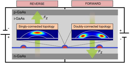
Given the different orbital confinement found in singly and doubly connected potentials, nanostructures with electrically tunable topology might be of great interest to couple spin and orbital degrees of freedom. Llorens et al. (2015); Llorens and Alén (2018) In the following, we investigate such possibility focusing on type-II InAs/GaAsSb QDs grown on GaAs and embedded in a p-i-n diode structure. For Sb molar fractions beyond 16, the band alignment changes from type-I to type-II, with the electron confined inside the InAs and the hole delocalized in the GaAsSb overlayer. Akahane et al. (2004); Ripalda et al. (2005); Liu et al. (2005). The resulting wave function configuration brings two important assets. Firstly, the weak localization of the hole results in a larger exciton polarizability or, in other words, a higher tunability of the exciton energy. Voltage control of the exciton dipole moment in the vertical direction thus allows large tuning of the radiative lifetime. Llorens et al. (2015); Heyn et al. (2018) Secondly, we shall see that, pushing or pulling the hole against the bounding interfaces of the overlayer, also brings a topological change in the hole ground state wave function as schematically shown in Figure 1. By this manipulation we are in fact engineering the wave function density of probability from dot- to ring-like as originally discussed in Ref. Kleemans et al., 2007
The rest of the paper is organized as follows. The details of the sample and optical characterization are summarized in Section II. We present in Section III the magneto-optical photoluminescence results. We first find that both, the diamagnetic coefficient and the -factor, can be modulated by the applied bias. Then, we report oscillations of the emission intensity and the degree of circular polarization () with the applied magnetic field which occur only under forward bias. We discuss these effects in Section IV, relying on two different theoretical models. The first one is described in Section IV.1. It consists of a multiband axisymmetric model which provides a quantitative evolution of the orbital related effects: the diamagnetic coefficient dependence and the intensity oscillation. The limitation of the axial symmetry of this model is complemented with an effective mass model in Section IV.2. It is based on a parabolic confinement which can analytically evolve from a dot-like to a ring-like potential and includes an eccentricity parameter. From the solutions of this model, we discuss the spin related results (-factor and ) in Section IV.3 by including the Rashba contribution in the Hamiltonian.
II Experimental details
II.1 Sample and device
A p-i-n diode was grown by molecular beam epitaxy (MBE) on a n-type GaAs (001) substrate. The intrinsic GaAs region spans 400 nm embedding in its center a single layer of self-assembled InAs QDs. After the formation of the QDs, they were covered by a 6-nm-thick GaAsSb layer with 28 nominal content of Sb. More details about the growth recipe and the morphological changes induced by rapid thermal annealing (RTA) treatment of these QDs can be found elsewhere. Ulloa et al. (2012a) After the RTA treatment, mesas of different sizes and ohmic contacts were defined by conventional optical lithography techniques.
II.2 Optical characterization
To investigate OABE in our sample, magneto-photoluminescence (MPL) spectra were recorded at 5 K in the Faraday configuration up to 9 T. To avoid unnecessary manipulations, the light polarization was analyzed in the circular basis reversing the magnetic field direction. After the circular polarization analyzer, the emission was coupled into a multimode optical fibre and then imaged into the 100-m-wide slits of a 300 mm focal length monochromator (1200 lines/mm grating). The light intensity was measured with a peltier cooled InGaAs photomultiplier connected to a lock-in amplifier. For every magnetic field, a PL spectrum was recorded for ,1, 0, 1 and 1.35 (corresponding to 88, 63, 38, 13 and 4.2 kV cm-1, respectively). 0 ( 0) corresponds to reverse (forward) bias as indicated in Fig. 1 The power of the temperature stabilized 690 nm diode laser was registered simultaneously being its value constant within % during the whole experiment and within 0.2% while scanning the voltage at fixed magnetic field. Each spectrum was normalized by its corresponding excitation power and then analyzed by Gaussian deconvolution.
III Bias Dependent Magneto-Photoluminescence Experiments
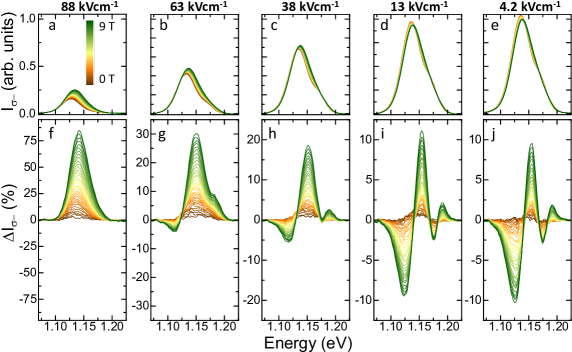
Figure 2(a-e) shows the evolution of the -polarized MPL spectra in vertical electrical fields () between 88 and 4.2 kV cm-1. To highlight the magnetic field effects, the lower panels of Figure 2 show the evolution after subtraction and normalization by the spectrum at 0 T. In our previous work, we investigated the electric field response at 0 T of the type-II InAs/GaAsSb QD system. Llorens et al. (2015) A large reverse bias increases the electron tunneling rate out of the InAs quantum dot potential towards the GaAs barrier. This leads to a noticeable intensity quenching moving to the left in the upper panel of Figure 2. The electric field also reduces the electron-hole overlap and red shifts the peak emission energy at 0 T. In the following, we focus on the changes produced by in the magnetic response of the sample. To maintain an unified description, the excitation conditions were kept approximately the same in the experiments of Ref. Llorens et al., 2015 and here. Thus, the PL emission comprises two bands which are split by 36 meV at 0 V and 0 T. These bands arise from the ground state and bright excited state recombinations, both inhomogeneously broadened. Their integrated intensity ratio varies with and is always larger than 7.
The magnetic properties will be discussed attending solely to the evolution of the PL near the ground state of the system. For every , the and MPL spectra were recorded up to 9 T. Gaussian deconvolution was then applied to extract the overall evolution of the ground state emission. From the deconvoluted MPL peak energy, , and integrated intensity, , we obtain the average energy shift, , unpolarized integrated intensity, , Zeeman splitting, , and degree of circular polarization, for the low energy band alone.
Figure 3 gathers the diamagnetic energy shift and Zeeman splitting for different electric fields. Solid lines are quadratic and linear fittings to and , respectively, where is the Bohr magneton, and and represent the diamagnetic shift coefficient and Landé -factor for the type-II exciton, respectively. Hayne and Bansal (2012) Both functions describe accurately the data, except for a linear deviation for in the strong tunneling regime corresponding to relatively large electric fields in Figs. 3(a-b). We observe that both and are affected by the external electric field and also that oscillations in magnetic field are absent for the ground state peak energy. In this bias range, the -factor variation is and shall be attributed to a voltage modulation of the spin-orbit interaction as it will be discussed in detail in Section IV.3.
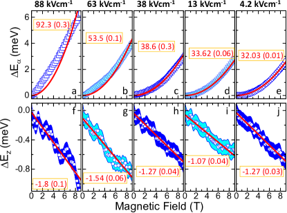
The variation is even more pronounced and exhibits a clear diminishing trend reducing the reverse bias. For a magnetic field applied in the growth direction, the diamagnetic shift is usually associated with the exciton wave function extension in the growth plane. Nash et al. (1989) However, this simple correlation between exciton diameter and diamagnetic shift magnitude is lost when electronic levels with different angular momentum cross each other in the fundamental state. These level crossings are the source of the interference between different quantum paths leading to AB magneto-oscillations in quantum rings. Fomin (2014) In an ensemble experiment, they might be obscured by inhomogeneous effect but might reveal themselves as a flattening of and the observed evolution of vs. . In our case, the tunneling also becomes more important as the positive field increases. In these conditions, the electron wave function penetrates in the barrier and might also affect the value of . These issues shall be discussed in detail in the next sections.
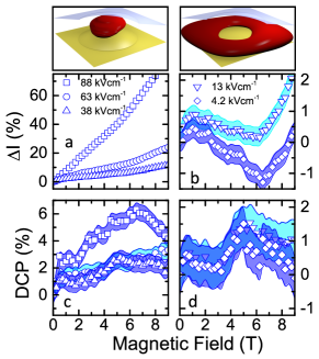
The evolution of the unpolarized integrated intensity after subtraction and normalization by the 0 T value, , and the are depicted in Figure 4. At large electric fields, increases with exhibiting a strong magnetic brightening up to 75% [Figure 4(a)]. The dependence follows a fixed linear slope with small oscillations which are only apparent in the first derivative of the data (not shown). By reducing , the magnetic brightening effect diminishes and, below 13 kV cm-1, an oscillatory behavior develops [Figure 4(b)]. In the same bias range, the is positive, as expected from the negative -factor, and evolves with magnetic field from a rather monotonic dependence at 83 kV cm-1 to a clearly oscillatory one at 4.2 kV cm-1.
IV Discussion
In the quantum ring literature, MPL intensity oscillations are related to changes in the ground state angular momentum arising from the OABE. Fomin (2014) Voltage modulation of such oscillations have been reported for type-I InAs/GaAs single quantum rings, Ding et al. (2010); Li and Peeters (2011) and also predicted for 2D materials. de Sousa et al. (2017) The modulation must be associated to changes in the effective quantum ring confinement potential. In the type-II InAs/GaAsSb QD system, holes are spatially localized within the GaAsSb layer near the InAs QDs. Llorens et al. (2015); Ulloa et al. (2010, 2012b); Klenovský et al. (2010); Hospodková et al. (2013); Liu et al. (2005) The strain distribution and electron-hole Coulomb interaction create a net attractive potential for the hole that is balanced by the InAs/GaAsSb and GaAs/GaAsSb valence band offsets. An external electric field modulates the geometry of this potential and, in turn, a change of the hole wave function topology from singly to doubly connected is expected. The inset in Figure 4 represents the qualitative evolution of the hole probability density according to the theoretical description developed on Ref. Llorens et al., 2015.
IV.1 Axially symmetric model
To analyze our data quantitatively, we start with an axially symmetric model for the type-II InAs/GaAsSb QD system. Under this approximation, the total angular momentum is a good quantum number for the exciton states and allows a proper labeling scheme. The whole Hamiltonian including the strain is forced to be axially symmetric. Hence, even in the multiband case, the states are labeled according to the -projection of the total angular momentum (). In case of small band mixing, the state can also be labeled with the -projection of the orbital angular momentum of the envelope function associated with the main Bloch component (). Further details and explicit expressions can be found in the Appendix A.
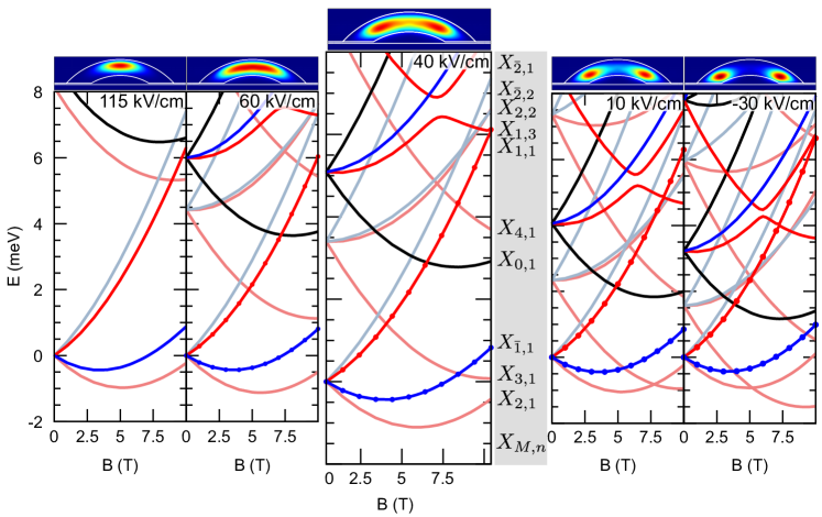
The numerical results are obtained for a quantum dot of the same size and composition as those analyzed in our previous studies Ulloa et al. (2012a); Llorens et al. (2015). The geometry of the InGaAs QD is a lens shape of radius nm and height nm. It sits on top of a 0.5 nm InGaAs wetting layer (WL) and is surrounded by a GaAsSb shell of 6 nm thickness which plays the role of the overlayer. The composition of the nanostructure is Ga0.25In0.75As and that of the overlayer GaAs0.80Sb0.20.
Figure 5 shows the results in the exciton picture. Each electron (hole) state is defined by the quantum number introduced in Eq. (6). Hence, the exciton states are defined by the addition of the total angular momentum of the constitutive particles (-projections). The only optically active exciton states are those characterized by . The emitted photons are polarized along the direction for and circularly polarized for . We have selected five values of the electric field which fully cover the topological transition from dot to ring. For clarity, we have added a contour plot of the hole probability density on top of each energy level dispersion. One can easily distinguish the localization of the hole particle on top of the nanostructure (115 kV cm-1) and its drift towards the base as the electric field diminishes. The corresponding exciton states are indicated only for the central panel as , being the exciton total angular momentum -projection and the principal quantum number of that particular manifold. We first focus on the dispersion for kV cm-1 (large reverse bias). At T, the ground state is composed of the fourth-fold degenerated quadruplet with and and . The magnetic field splits this level into four branches. The can be distinguished by the non-zero radiative rate (dots over the line) and more intense colored lines used in the representation. These four exciton states result of the combination of two electron and two hole states whose dominant Bloch amplitudes are and . The envelope function of each dominant Bloch amplitudes is defined by . This explains the weak dependence of the internal structure of the quadruplet to the electric field and hence to the topology of the hole wave function. Irrespective of whether the hole is located above the apex of the QD ( kV cm-1) or close to its base ( kV cm-1) the energy levels are weakly perturbed. On the contrary, the quantization energy of the excited states is significantly perturbed by the electric field. The first excited state at T is out the plot for kV cm-1, while at kV cm-1 the energy splitting with the ground state is meV. This clearly illustrates how the electric field efficiently modifies the angular and radial confinement exerted on the hole wave function. In theses states, the dominant envelope wave functions of the hole is characterized by and therefore are more sensitive to the vertical position within the overlayer.
Figure 5 illustrates that the applied electric field can effectively isolate the ground state from the excited states for kV cm-1 or bunch excited and ground states together for kV cm-1. In the bunching regime, the model predicts the crossing between states of different , and thus a change in the ground state orbital confinement. More explicitly, the high energy state and the and low energy states cross at and 7.8 T for kV cm-1, respectively. These crossings occur at fields within the range of the experimental values presented before. This would result in the possibility of observing experimentally, at least, the crossing between and the states of lower energy and thus an associated optical AB oscillation. The precise correspondence with the experimental results is difficult to establish given that its observation would depend on the thermalization of the excited carriers and the eventual relaxation of the selection rules in the actual QDs, as explained below. As expected for AB related effects, the number of crossings and their actual positions depend on the exciton in-plane dipole moment which, in our case, decreases with the electric field. In view of these results, the oscillatory dependence observed for the unpolarized integrated intensity and in Fig. 4 is a consequence of a change in the total angular momentum of the ground state and hence a signature of the OABE.
The inhomogeneous broadening of the MPL spectra in Sec. III prevents the observation of the individual energy levels shown in Fig. 5, thus peak energy magneto-oscillations cannot be detected in our experiment. Kim et al. (2016) This notwithstanding, our analysis of the emission energy shifts in Figures 3(a-e) revealed a three fold increase of the diamagnetic shift coefficient with the electric field. From the numerical results shown in Figure 5, we can calculate this magnitude for the bright exciton states. The resulting coefficients for the electron , hole and exciton are shown independently in Figure 6.
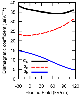
The hole diamagnetic shift decreases from 15 to 5 by increasing the electric field from -30 to 115 kV cm-1. This is expected since, during the hole drift from the base towards the apex of the overlayer, its density of probability shrinks decreasing (see contour plot insets in Fig. 5). Nash et al. (1989) In the same bias range, goes from from 23 to 32 , increasing with the reverse bias. This is a consequence of the spill-over of the electron wave function in the GaAs barrier underneath. For kV cm-1, electron tunneling out of the InAs QD becomes noticeable. Llorens et al. (2015) The numerical model catches this situation only approximately and, for the largest bias, the calculated is only 37 , while experimentally is 92.3 . Indeed, for kV cm-1, the experimental dispersion becomes increasingly linear. Linear dispersion is characteristic of the Landau regime. In our context, it corresponds to a weaker confinement as a result of the delocalization of the electron wave function as the tunnel regime becomes dominant [see Figs. 3(a,b)]. In the opposite bias regime, the correspondence with the experimental values is much better. (32.62 ) is found at kV cm-1 while renders 36.05 . As shown in Fig. 5, in this bias range, the ground state of the electron-hole system is composed mostly of states with angular momentum . Under the axially symmetric approximation, these states are purely dark and do not contribute to . If the symmetry of the actual confinement potential is broken, they can achieve oscillator strength, lower further the diamagnetic shift and produce AB intensity oscillation, as discussed in the next Section.
IV.2 In plane asymmetry effects
It has been profusely reported that quantum dot elongation can take place after capping. The strain fields that build up during this process provoke the anisotropic segregation of In atoms leading to an eccentricity increase of previously cylindrical systems. Alonso-Álvarez et al. (2013); Teodoro et al. (2012) Analogous process is also triggered during the synthesis of type-II InAs/GaAsSb quantum dots which also might lead to anisotropic piezoelectric fields. Klenovský et al. (2010); Krapek et al. (2015) Thus, it is a goal of our following discussion to assess the effects of in-plane confinement anisotropy in the electronic properties. To this end, we introduce an effective mass description of both the conduction and valence bands, and incorporate the effects of confinement asymmetry for electrons and holes in a model that can emulate quantum dots and rings within the same framework, as well as the resulting Rashba spin-orbit coupling fields arising from confinement and external fields.
The eigen-value problem for the conduction band will be solved by expanding the corresponding wave functions in the basis of the eigen-solutions of the following effective mass Hamiltonian,
| (1) |
with the effective mass, and the magnetic field pointing along the growth -direction, where is the Pauli matrix vector, and . For the unperturbed basis, will be assumed as a rigid wall potential profile while the in-plane confinement in polar coordinates takes the form: Tan and Inkson (1996)
| (2) |
which allows obtaining an exact solution that covers both the quantum ring and the quantum dot confinements. The parameters and define the structure shape and for , a ring with radius is obtained. In turn, by setting , a parabolic quantum dot with effective radius can be emulated. This potential allows us to describe effectively the change of topology on the hole as a result of the applied electric field.
For the valence band basis, used to expand the Luttinger Hamiltonian eigen-solutions, we use an analogous separable problem yet assuming anisotropic effective masses in Eq. (1), and replacing and , by and the angular momentum matrix for , , respectively.
The symmetry constrains can be subsequently relaxed by reshaping the in-plane confinement in the following way, . This is an extension of the profile proposed in Refs. Lopes-Oliveira et al., 2014, 2015, where the term controlled by the parameter determines the eccentricity of the outer rim of the confinement. The values of the eccentricity are given by , for , that corresponds to an elliptical shrinking, or for , that leads to an elliptical stretching. Additionally, an electric field along the growth direction can be considered by inserting the term into that will couple the wave function components of different parity. The details on the solution of the Schrödinger equation are in Appendix B. The asymmetric solution is given by the expansion
| (3) |
where labels the basis functions at the Brillouin zone center in the Kane model (, and ), is the -projection of the orbital angular momentum, is the radial quantum number and is the vertical quantum number. Thus, the expansion coefficients, , determine the spin character of the final state, namely, the degree of hybridization of the various components.
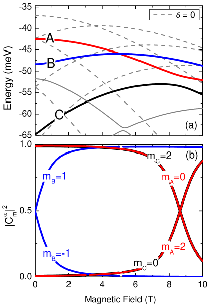
The eccentricity breaks the cylindrical symmetry. Figure 7(a) shows the impact of the symmetry break on the valence band energy levels for the first few states confined in a QR with nm and height nm. For this calculation, we have omitted the spin splitting. Dashed lines render the cylindrical case ( meV) mimicking the energy dispersion found in the previous section. Solid lines stand for an eccentric ring with meV. The only relevant energy levels for the discussion are represented with bold lines and labeled as A, B and C. The A and B levels cross at =4 T, and the A and C levels anti-cross at =7.5 T. The mixing of different -components reduces the effective diamagnetic shift of the valence band ground hybrid state. This mixing is quantified in Fig. 7(b), where the expansion coefficients resulting from the diagonalization of the valence band Hamiltonian have been depicted. In the symmetric case, the ground state experiences a sharp change at the crossing from a character to a (not shown). In contrast, in the eccentric case there are no discontinuities, reflecting a soft evolution of the wave function character with the magnetic field. The states corresponding to the energy levels A and C swap their character from to at the anti-crossing. The energy level B acquires a dominant character being insensitive to the crossing and anti-crossing.
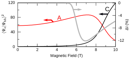
The changes of the electronic states energy and character modulate also the emission intensity, which can be calculated from the oscillator strength (OS). As the electron ground state has =0 character, the state B is optically inactive within the model, being its OS negligible. States A and C, however, show an exchange of oscillator strength as they approach the anti-crossing as shown in Figure 8. The smooth increase of the OS at high magnetic fields is attributed to the magnetic brightening. In this situation, we can calculate the emission intensity of the system solving a simple rate equations model based on Ref. Sugawara et al., 2002 as explained in Ref. Sup, . The radiative rates are parameters of the model and scale with the OS calculated for the states A and C. For state B, the pure dark condition is relaxed, since dark states must eventually recombine due to hybridization processes not considered here (e.g. electron-hole exchange). As shown in Figure 8, our model predicts an intensity oscillation around 7 T with similar phase but slightly larger amplitude than the experimental evolution displayed in Figure 4(b). It must be noted that the position of the crossings and the energy difference between states presents fluctuations among QDs. This shall lead to a shallower experimental oscillation resulting from the ensemble average of many curves like the ones shown in Figure 8. Teodoro et al. (2010)
IV.3 Spin-orbit coupling effects
We have just shown that the symmetry reduction in a quantum ring lowers the effective diamagnetic shift of the ground state as the angular momentum states become intermixed. In turn, including spin-orbit interaction terms, the electrical modulation of the lateral and vertical confinement also changes the spin states. Ares et al. (2013); Bennett et al. (2013); Corfdir et al. (2014); Jovanov et al. (2011); Klotz et al. (2010); Prechtel et al. (2015); Yang et al. (2015); Tholen et al. (2016) According to the results presented in Fig. 3(f-j), the exciton energy spin splitting increases with the device reverse bias. Meanwhile, within the GaAsSb overlayer, the hole wave function geometry and topology evolve. Both observations can be connected once the spin orbit interaction is incorporated to the model represented by Eqs. (1)-(3). The interaction is introduced through the Rashba contribution to the total Hamiltonian , for the conduction band, or , for the valence band. The expression for the spin orbit Hamiltonian assuming the confinement profile that includes all the asymmetry terms and the resulting energy corrections are given in Appendix C.
In turn, we can separate the spin-orbit effects induced by confinement and asymmetry into first or higher order contributions. The latter ones are produced by the coupling of previously unperturbed levels and appear strongly when these levels approach inducing (or enhancing) anticrossings, mostly at higher fields. The first order terms appear already at vanishing fields and may provoke, for instance, the tuning of the effective Landé factor. We shall focus the discussion on these ones.
The first order correction to the conduction band Zeeman splitting induced by the spin-orbit coupling can be calculated exactly for the ground state of a quantum dot according to: Cabral et al. (2017)
| (4) |
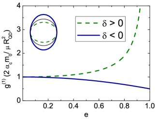
This result is depicted in Fig. 9 and illustrates how the Landé factor correction grows as the quantum dot volume is reduced by shortening or by shrinking the lateral confinement into an ellipse ( corresponds to an elliptical shrinking).
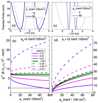
For a quantum ring, such a modulation is not trivial and depends on the way the confinement shape is modified as shown in Fig. 10. Note that by fixing and increasing , the quantum ring radius increases as a result of widening the inner rim [Fig. 10(a)]. Such a modulation of the confinement profile can either increase or decrease the valence band Landé factor correction according to the value of the eccentricity and the sign of as displayed in Fig. 10(b). For large enough rings, the eccentricity may even lead to an absolute reduction of the Landé factor. If in contrast, the parameter is fixed while increasing , the confinement potential shrinks as a result of the reduction of the external radius. This condition is plotted in Fig. 10(c) while the corresponding first order correction to the -factor appears in panel (d). Such a reduction of the quantum ring radius provokes a monotonic increase of this correction factor regardless the value of the eccentricity.
Through this model, the non-monotonic increase of the -factor displayed in Fig. 3 can be ascribed to the bias dependent shrinkage and symmetry reduction of the hole wave function. To assess the absolute values of the -factor correction, and the relevance of antimonides in that respect, we may contrast systems with different spin-orbit coupling: GaAs, GaSb and InSb, respectively. For the valence band of these materials, Å2, , . Their calculation is detailed in Appendix C. According to these values, the units used in Fig. 10 for the valence band Landé factor corrections are -0.012, for GaAs, -0.038, for GaSb, and -0.442, for InSb. In turn, for the conduction band Landé factor correction, plotted in Fig. 9 the units are radius dependent and for a pure InAs QD with nm they equal 1.6.
For electron-hole pairs confined in type-II nanostructures, the unperturbed effective Zeeman splitting can be obtained from, . In the case of an electron in InAs and a hole in GaAs0.8Sb0.2, the effective Landé factor is . By introducing the effects of confinement, the Landé factor can be corrected as . Note that according to the values of and , the correction leads to a Landé factor increase in relative terms towards more positive values. For low fields, the electrons and holes are confined in QD shapes with and =5 meV/100 nm2 for holes while =8 nm for electrons. This leads to Landé factor corrections of =1.6 and =0.129 for electrons and holes, respectively, leading to a total Landé factor =-1.891. At higher electric fields the hole wave function moves downwards, where we can expect a radius increase of an eccentric QR (=) with . This translates into the model by a growing from 0 to 10 meV100 nm2, with =5 meV/100 nm2, corresponding to the QR with =12 nm characterized in Fig. 7. According to Fig. 10(b), this results in an increase on the correction of =0.172. In turn, the electron is confined inside of the QD and it could move upwards, with a smaller effective =6.8 nm with respect to the situation of larger positive fields. In Eq. (4), is inversely proportional to and therefore increases its value to =2.21. This translates into a total Landé factor of =-1.23. The change in the estimation of the -factor between low and high fields agrees with the observed experimental change in from -1.8 to -1.3.
V Conclusions
In summary, we have presented experimental evidence on the tuning of the electronic structure of type-II InAs/GaAsSb quantum dots under vertical electric and magnetic fields. Induced by the external bias, the drift of the hole wave function in the soft confinement of the GaAsSb layer encompasses a wide range of geometrical and topological changes in the effective potential. These changes cannot be easily induced in type-I systems and provide a rich variety of insights on the way geometry affects the electronic structure and thus the optical response. The observed effects have been studied with theoretical approaches that include electronic confinement, strain fields and spin effects on the same footing. In particular, we report how the application of an external bias tunes the hole confinement geometry independently of the electron. Under certain bias conditions, the hole confinement topology changes and magnetic field oscillations are observed. The oscillations follow the orbital quantization of the hole state and are thus susceptible to the confinement size and eccentricity. Although further work is needed to put these ideas at work in single InAs/GaAsSb nanostructures, this modulation of hole orbital quantization, accompanied by the tuning of the exciton -factor, might pave the way for the voltage control of spin degrees of freedom as required by several quantum technologies.
Acknowledgements.
The authors gratefully acknowledge financial support from EURAMET through EMPIR program 17FUN06-SIQUST, from Spanish MINEICO through grants TEC2015-64189-C3-2-R, MAT2016-77491-C2-1-R, EUIN2017-88844 and RYC-2017-21995, from Comunidad de Madrid through grant P2018/EMT-4308, and from CSIC through grants I-COOP-2017-COOPB20320 and PTI-001. Support from Brazilian agencies is also acknowledged through FAPESP grant 2014/02112-3 and CNPq grant 306414/2015-5.Appendix A Details of the multi-band axisymmetric model
The electronic structure of the InAs/GaAsSb QDs is computed by the method folowing Trebin et al. Trebin et al. (1979); Winkler (2003) notation. The final Hamiltonian is the result of adding three contribution, the term (), the strain interactions (Bir-Pikus ) and the magnetic interactions ():
| (5) |
We have neglected the linear terms in the valence-valence interaction, the quadratic and terms in the conduction-valence interaction and the in the strain-induced interactions. To simplify the analysis, we have imposed axial symmetry in all the terms involved in the Hamiltonian. This approximation also affects the strain distribution forcing us to consider the materials as elastically isotropic. Compact expressions are obtained with the Eshelby’s inclusions method Eshelby (1957) and Fourier transform of the strain tensor Andreev et al. (1999). With this formalism we succeeded in explaining Raman frequency shifts induced by the strain Cros et al. (2006); Garro et al. (2006) and strain distributions extracted from middle energy ion scattering Jalabert et al. (2005) experiments. The solution of the problem is obtained considering that only the band edges are discontinuous across material interfaces. To describe electrons and holes properly in type-II QDs, we have decoupled the conduction and valence bands in . Hence, the electrons are described by a single band model, while a Hamiltonian is used for the holes.
Axial symmetry allows us to define a total angular momentum of component , which is the result of adding the corresponding components of the envelope function orbital angular momentum () and Bloch’s amplitude total angular momentum (): . Each electronic state is described by the wave function
| (6) |
where is the Bloch amplitude of the band at the origin of the Brillouin zone and is the envelope function associated to the Bloch component. The envelope function in expressed cylindrical coordinates defined by a phase factor characterized by and a two dimensional component .
The solution of the Schrödinger equation is obtained by expanding Eq. (6) in a complete basis. The basis is defined by the eigenfunctions of a hard-wall cylinder:
| (7) |
where is the Bessel function of order , is its zero number , , and are the radius and height of the expansion cylinder and
| (8) |
is the normalization of the radial part. This definitions ensure the orthonormality of the expansion basis. A similar procedure was followed by Tadić et al. in Refs. Tadić et al., 2002; Tadić and Peeters, 2005. Further details can be found in Ref. Llorens Montolio, 2007.
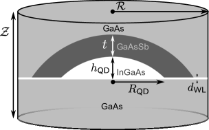
In Figure 11, we show an outline of the QD embedded in the overlayer enclosed by the expansion cylinder. The number of geometrical parameters is therefore reduced to six.
Appendix B Details of the EMA non-axisymmetric model
The solution for the 3D Schrödinger equation, , corresponding to the potential profile in Eq. (2) is given by
| (9) |
where is the wave function for a rigid square well and are the basis functions at the Brillouin zone center in the Kane model: and for the electron and heavy hole, respectively. The planar wave function has the form
| (10) | ||||
where is the confluent hypergeometric function, is the radial quantum number, is the vertical quantum number, and labels the angular momentum. The corresponding eigen-energies for the 3D problem are
| (11) |
with , , , and .
Appendix C Details of the SOC non-axisymmetric model
The expression for the spin orbit Hamiltonian assuming the confinement profile that includes all the asymmetry terms is given by:
| (12) |
with , being the components of the Pauli matrices. The spin orbit Hamiltonian for the valence band can be readily obtained by replacing these matrices with those for angular momentum and by .
We can extract from Eq. (12) the diagonal terms that contribute to the first order renormalization of the spin-splitting of the ground state with for the limit , , in the basis of unperturbed states introduced by Eq. (9). The zero order value is essentially the Zeeman splitting given by
| (13) |
in the case of the conduction band, while for the valence band stands as
| (14) |
In the case of a conduction band electron confined within a QD potential, , the first order contribution of the spin-orbit interaction, in the limit of low fields, can be reduced to
| (15) |
Meanwhile, for the valence band and a quantum ring profile, , the expression reads
| (16) |
This allows introducing the first order correction to the Landé factor defined as and shown in Fig. 9 and 10 in the article, respectively. With them, one may now assess the relative effect of the confinement geometry and topology change on the spin splitting. The calculation of the Rashba coefficient appearing in Eq.(16) is computed from the band parameters in Table 1 and the expression:
| (17) |
which is defined as in Winkler, 2003.
Appendix D Material parameters
The material band parameters are extracted from Vurgaftman et al. (2001). Magnetic related parameters are shown in Table 1. The values of the compounds GaInAs and GaAsSb are obtained through linear interpolation when no bowing parameters is reported.
| GaAs | InAs | GaSb | |
|---|---|---|---|
| -0.44 | -14.9 | -9.25 | |
| 1.20 | 7.60 | 4.60 | |
| 0.01 | 0.39 | 0.00 | |
| (eV) | 1.519 | 0.418 | 0.813 |
| (eV) | 4.488 | 4.390 | 3.3 |
| (eV) | 0.341 | 0.380 | 0.750 |
| (eV) | 0.171 | 0.240 | 0.330 |
| (eVÅ) | 10.493 | 9.197 | 9.504 |
| (eVÅ) | 4.780 | 0.873 | 3.326 |
| (eVÅ) | 8.165 | 8.331 | 8.121 |
References
- Michler (2017) P. Michler, ed., Quantum Dots for Quantum Information Technologies, Nano-Optics and Nanophotonics (Springer International Publishing, 2017).
- Nadj-Perge et al. (2012) S. Nadj-Perge, V. S. Pribiag, J. W. G. van den Berg, K. Zuo, S. R. Plissard, E. P. A. M. Bakkers, S. M. Frolov, and L. P. Kouwenhoven, Spectroscopy of Spin-Orbit Quantum Bits in Indium Antimonide Nanowires, Phys. Rev. Lett. 108, 166801 (2012).
- Atatüre et al. (2006) M. Atatüre, J. Dreiser, A. Badolato, A. Högele, K. Karrai, and A. Imamoglu, Quantum-Dot Spin-State Preparation with Near-Unity Fidelity, Science 312, 551 (2006).
- Brunner et al. (2009) D. Brunner, B. D. Gerardot, P. A. Dalgarno, G. Wüst, K. Karrai, N. G. Stoltz, P. M. Petroff, and R. J. Warburton, A Coherent Single-Hole Spin in a Semiconductor, Science 325, 70 (2009).
- Vidal et al. (2016) M. Vidal, M. V. Durnev, L. Bouet, T. Amand, M. M. Glazov, E. L. Ivchenko, P. Zhou, G. Wang, T. Mano, T. Kuroda, X. Marie, K. Sakoda, and B. Urbaszek, Hyperfine coupling of hole and nuclear spins in symmetric (111)-grown GaAs quantum dots, Phys. Rev. B 94, 121302 (2016).
- Nowack et al. (2007) K. C. Nowack, F. H. L. Koppens, Y. V. Nazarov, and L. M. K. Vandersypen, Coherent Control of a Single Electron Spin with Electric Fields, Science 318, 1430 (2007).
- Pingenot et al. (2008) J. Pingenot, C. E. Pryor, and M. E. Flatté, Method for full Bloch sphere control of a localized spin via a single electrical gate, Appl. Phys. Lett. 92, 222502 (2008).
- Andlauer and Vogl (2009) T. Andlauer and P. Vogl, Electrically controllable tensors in quantum dot molecules, Phys. Rev. B 79, 045307 (2009).
- Pingenot et al. (2011) J. Pingenot, C. E. Pryor, and M. E. Flatté, Electric-field manipulation of the Landé tensor of a hole in an In0.5Ga0.5As/GaAs self-assembled quantum dot, Phys. Rev. B 84, 195403 (2011).
- Tholen et al. (2016) H. M. G. A. Tholen, J. S. Wildmann, A. Rastelli, R. Trotta, C. E. Pryor, E. Zallo, O. G. Schmidt, P. M. Koenraad, and A. Y. Silov, Strain-induced -factor tuning in single InGaAs/GaAs quantum dots, Phys. Rev. B 94, 245301 (2016).
- Klotz et al. (2010) F. Klotz, V. Jovanov, J. Kierig, E. C. Clark, D. Rudolph, D. Heiss, M. Bichler, G. Abstreiter, M. S. Brandt, and J. J. Finley, Observation of an electrically tunable exciton factor in InGaAs/GaAs quantum dots, Appl. Phys. Lett. 96, 053113 (2010).
- Jovanov et al. (2011) V. Jovanov, T. Eissfeller, S. Kapfinger, E. C. Clark, F. Klotz, M. Bichler, J. G. Keizer, P. M. Koenraad, G. Abstreiter, and J. J. Finley, Observation and explanation of strong electrically tunable exciton factors in composition engineered In(Ga)As quantum dots, Phys. Rev. B 83, 161303 (2011).
- Ares et al. (2013) N. Ares, V. N. Golovach, G. Katsaros, M. Stoffel, F. Fournel, L. I. Glazman, O. G. Schmidt, and S. De Franceschi, Nature of Tunable Hole Factors in Quantum Dots, Phys. Rev. Lett. 110, 046602 (2013).
- Corfdir et al. (2014) P. Corfdir, Y. Fontana, B. Van Hattem, E. Russo-Averchi, M. Heiss, A. Fontcuberta i Morral, and R. T. Phillips, Tuning the g-factor of neutral and charged excitons confined to self-assembled (Al, Ga)As shell quantum dots, Appl. Phys. Lett. 105, 223111 (2014).
- Godden et al. (2012) T. M. Godden, J. H. Quilter, A. J. Ramsay, Y. Wu, P. Brereton, I. J. Luxmoore, J. Puebla, A. M. Fox, and M. S. Skolnick, Fast preparation of a single-hole spin in an InAs/GaAs quantum dot in a Voigt-geometry magnetic field, Phys. Rev. B 85, 155310 (2012).
- Bennett et al. (2013) A. J. Bennett, M. A. Pooley, Y. Cao, N. Sköld, I. Farrer, D. A. Ritchie, and A. J. Shields, Voltage tunability of single-spin states in a quantum dot, Nat. Commun. 4, 1522 (2013).
- Prechtel et al. (2015) J. H. Prechtel, F. Maier, J. Houel, A. V. Kuhlmann, A. Ludwig, A. D. Wieck, D. Loss, and R. J. Warburton, Electrically tunable hole factor of an optically active quantum dot for fast spin rotations, Phys. Rev. B 91, 165304 (2015).
- Fomin (2014) V. M. Fomin, ed., Physics of Quantum Rings (Springer Berlin Heidelberg, 2014).
- Lorke et al. (2000) A. Lorke, R. Johannes Luyken, A. O. Govorov, J. P. Kotthaus, J. M. Garcia, and P. M. Petroff, Spectroscopy of Nanoscopic Semiconductor Rings, Phys. Rev. Lett. 84, 2223 (2000).
- Fuhrer et al. (2001) A. Fuhrer, K. Ensslin, M. Bichler, S. Lüscher, T. Heinzel, T. Ihn, and W. Wegscheider, Energy spectra of quantum rings, Nature 413, 822 (2001).
- Ribeiro et al. (2004) E. Ribeiro, A. O. Govorov, W. Carvalho, and G. Medeiros-Ribeiro, Aharonov-Bohm signature for neutral polarized excitons in type-II quantum dot ensembles, Phys. Rev. Lett. 92, 126402 (2004).
- Dias da Silva et al. (2005) L. G. G. V. Dias da Silva, S. E. Ulloa, and T. V. Shahbazyan, Polarization and Aharonov-Bohm oscillations in quantum-ring magnetoexcitons, Phys. Rev. B 72, 125327 (2005).
- Kleemans et al. (2007) N. A. J. M. Kleemans, I. M. A. Bominaar-Silkens, V. M. Fomin, V. N. Gladilin, D. Granados, A. G. Taboada, J. M. García, P. Offermans, U. Zeitler, P. C. M. Christianen, J. C. Maan, J. T. Devreese, and P. M. Koenraad, Oscillatory Persistent Currents in Self-Assembled Quantum Rings, Phys. Rev. Lett. 99, 146808 (2007).
- Kuskovsky et al. (2007) I. L. Kuskovsky, W. MacDonald, A. O. Govorov, L. Mourokh, X. Wei, M. C. Tamargo, M. Tadic, and F. M. Peeters, Optical Aharonov-Bohm effect in stacked type-II quantum dots, Phys. Rev. B 76, 035342 (2007).
- Sellers et al. (2008) I. R. Sellers, V. R. Whiteside, I. L. Kuskovsky, A. O. Govorov, and B. D. McCombe, Aharonov-Bohm excitons at elevated temperatures in type-II ZnTe/ZnSe quantum dots, Phys. Rev. Lett. 100, 136405 (2008).
- Teodoro et al. (2010) M. D. Teodoro, V. L. Campo Jr., V. Lopez-Richard, E. Marega Jr., G. E. Marques, Y. Galvão Gobato, F. Iikawa, M. J. S. P. Brasil, Z. Y. AbuWaar, V. G. Dorogan, Y. I. Mazur, M. Benamara, and G. J. Salamo, Aharonov-Bohm Interference in Neutral Excitons: Effects of Built-In Electric Fields, Phys. Rev. Lett. 104, 086401 (2010).
- Miyamoto et al. (2010) S. Miyamoto, O. Moutanabbir, T. Ishikawa, M. Eto, E. E. Haller, K. Sawano, Y. Shiraki, and K. M. Itoh, Excitonic Aharonov-Bohm effect in isotopically pure 70Ge/Si self-assembled type-II quantum dots, Phys. Rev. B 82, 073306 (2010).
- Kim et al. (2016) H. D. Kim, R. Okuyama, K. Kyhm, M. Eto, R. A. Taylor, A. L. Nicolet, M. Potemski, G. Nogues, L. S. Dang, K.-C. Je, J. Kim, J.-H. Kyhm, K. H. Yoen, E. H. Lee, J. Y. Kim, I. K. Han, W. Choi, and J. Song, Observation of a Biexciton Wigner Molecule by Fractional Optical Aharonov-Bohm Oscillations in a Single Quantum Ring, Nano Lett. 16, 27 (2016).
- Aharonov and Bohm (1959) Y. Aharonov and D. Bohm, Significance of electromagnetic potentials in the quantum theory, Phys. Rev. 115, 485 (1959).
- Govorov et al. (2002) A. O. Govorov, S. E. Ulloa, K. Karrai, and R. J. Warburton, Polarized excitons in nanorings and the optical Aharonov-Bohm effect, Phys. Rev. B Rapid Comm. 66, 081309R (2002).
- Bayer et al. (2003) M. Bayer, M. Korkusinski, P. Hawrylak, T. Gutbrod, M. Michel, and A. Forchel, Optical Detection of the Aharonov-Bohm Effect on a Charged Particle in a Nanoscale Quantum Ring, Phys. Rev. Lett. 90, 186801 (2003).
- Okuyama et al. (2011) R. Okuyama, M. Eto, and H. Hyuga, Optical Aharonov-Bohm effect on Wigner molecules in type-II semiconductor quantum dots, Phys. Rev. B 83, 195311 (2011).
- Llorens and Alén (2018) J. M. Llorens and B. Alén, Wave-Function Topology Effects on Charged Excitons in Type-II InAs/GaAsSb Quantum Dots and Rings, Phys. Status Solidi RRL , 1800314 (2018).
- Llorens et al. (2015) J. M. Llorens, L. Wewior, E. R. C. d. Oliveira, J. M. Ulloa, A. D. Utrilla, A. Guzmán, A. Hierro, and B. Alén, Type-II InAs/GaAsSb quantum dots: Highly tunable exciton geometry and topology, Appl. Phys. Lett. 107, 183101 (2015).
- Akahane et al. (2004) K. Akahane, N. Yamamoto, and N. Ohtani, Long-wavelength light emission from InAs quantum dots covered by GaAsSb grown on GaAs substrates, Physica E 21, 295 (2004).
- Ripalda et al. (2005) J. M. Ripalda, D. Granados, Y. González, A. M. Sánchez, S. I. Molina, and J. M. García, Room temperature emission at 1.6 m from InGaAs quantum dots capped with GaAsSb, Appl. Phys. Lett. 87, 202108 (2005).
- Liu et al. (2005) H. Y. Liu, M. J. Steer, T. J. Badcock, D. J. Mowbray, M. S. Skolnick, P. Navaretti, K. M. Groom, M. Hopkinson, and R. A. Hogg, Long-wavelength light emission and lasing from InAs/GaAs quantum dots covered by a GaAsSb strain-reducing layer, Appl. Phys. Lett. 86, 143108 (2005).
- Heyn et al. (2018) C. Heyn, A. Küster, M. Zocher, and W. Hansen, Field-Controlled Quantum Dot to Ring Transformation in Wave-Function Tunable Cone-Shell Quantum Structures, Phys. Status Solidi RRL , 1800245 (2018).
- (39) See the supplemental material at https://journals.aps.org/prapplied for the MPL and rate equations details.
- Ulloa et al. (2012a) J. M. Ulloa, J. M. Llorens, B. Alén, D. F. Reyes, D. L. Sales, D. González, and A. Hierro, High efficient luminescence in type-II GaAsSb-capped InAs quantum dots upon annealing, Appl. Phys. Lett. 101, 253112 (2012a).
- Hayne and Bansal (2012) M. Hayne and B. Bansal, High-field magneto-photoluminescence of semiconductor nanostructures: High-field magneto-PL of semiconductor nanostructures, Luminescence 27, 179 (2012).
- Nash et al. (1989) K. J. Nash, M. S. Skolnick, P. A. Claxton, and J. S. Roberts, Diamagnetism as a probe of exciton localization in quantum wells, Phys. Rev. B 39, 10943 (1989).
- Ding et al. (2010) F. Ding, N. Akopian, B. Li, U. Perinetti, A. Govorov, F. M. Peeters, C. C. Bof Bufon, C. Deneke, Y. H. Chen, A. Rastelli, O. G. Schmidt, and V. Zwiller, Gate controlled Aharonov-Bohm-type oscillations from single neutral excitons in quantum rings, Phys. Rev. B 82, 075309 (2010).
- Li and Peeters (2011) B. Li and F. M. Peeters, Tunable optical Aharonov-Bohm effect in a semiconductor quantum ring, Phys. Rev. B 83, 115448 (2011).
- de Sousa et al. (2017) G. O. de Sousa, D. R. da Costa, A. Chaves, G. A. Farias, and F. M. Peeters, Unusual quantum confined Stark effect and Aharonov-Bohm oscillations in semiconductor quantum rings with anisotropic effective masses, Phys. Rev. B 95, 205414 (2017).
- Ulloa et al. (2010) J. M. Ulloa, R. Gargallo-Caballero, M. Bozkurt, M. del Moral, A. Guzmán, P. M. Koenraad, and A. Hierro, GaAsSb-capped InAs quantum dots: From enlarged quantum dot height to alloy fluctuations, Phys. Rev. B 81, 165305 (2010).
- Ulloa et al. (2012b) J. M. Ulloa, J. M. Llorens, M. del Moral, M. Bozkurt, P. M. Koenraad, and A. Hierro, Analysis of the modified optical properties and band structure of GaAs1-xSbx-capped InAs/GaAs quantum dots, J. Appl. Phys. 112, 074311 (2012b).
- Klenovský et al. (2010) P. Klenovský, V. Křápek, D. Munzar, and J. Humlíček, Electronic structure of InAs quantum dots with GaAsSb strain reducing layer: Localization of holes and its effect on the optical properties, Appl. Phys. Lett. 97, 203107 (2010).
- Hospodková et al. (2013) A. Hospodková, M. Zíková, J. Pangrác, J. Oswald, J. Kubištová, K. Kuldová, P. Hazdra, and E. Hulicius, Type I-type II band alignment of a GaAsSb/InAs/GaAs quantum dot heterostructure influenced by dot size and strain-reducing layer composition, J. Phys. D: Appl. Phys. 46, 095103 (2013).
- Alonso-Álvarez et al. (2013) D. Alonso-Álvarez, B. Alén, J. M. Ripalda, A. Rivera, A. G. Taboada, J. M. Llorens, Y. González, L. González, and F. Briones, Strain driven migration of In during the growth of InAs/GaAs quantum posts, APL Mater. 1, 022112 (2013).
- Teodoro et al. (2012) M. D. Teodoro, A. Malachias, V. Lopes-Oliveira, D. F. Cesar, V. Lopez-Richard, G. E. Marques, E. Marega, M. Benamara, Y. I. Mazur, and G. J. Salamo, In-plane mapping of buried InGaAs quantum rings and hybridization effects on the electronic structure, J. Appl. Phys. 112, 014319 (2012).
- Krapek et al. (2015) V. Krapek, P. Klenovsky, and T. Sikola, Excitonic fine structure splitting in type-II quantum dots, Phys. Rev. B 92, 195430 (2015).
- Tan and Inkson (1996) W.-C. Tan and J. C. Inkson, Electron states in a two-dimensional ring - an exactly soluble model, Semicond. Sci. Technol. 11, 1635 (1996).
- Lopes-Oliveira et al. (2014) V. Lopes-Oliveira, Y. I. Mazur, L. D. de Souza, L. A. B. Marçal, J. Wu, M. D. Teodoro, A. Malachias, V. G. Dorogan, M. Benamara, G. G. Tarasov, E. Marega, G. E. Marques, Z. M. Wang, M. Orlita, G. J. Salamo, and V. Lopez-Richard, Structural and magnetic confinement of holes in the spin-polarized emission of coupled quantum ring-quantum dot chains, Phys. Rev. B 90, 125315 (2014).
- Lopes-Oliveira et al. (2015) V. Lopes-Oliveira, L. K. Castelano, G. E. Marques, S. E. Ulloa, and V. Lopez-Richard, Berry phase and Rashba fields in quantum rings in tilted magnetic field, Phys. Rev. B 92, 035441 (2015).
- Sugawara et al. (2002) M. Sugawara, T. Akiyama, N. Hatori, Y. Nakata, H. Ebe, and H. Ishikawa, Quantum-dot semiconductor optical amplifiers for high-bit-rate signal processing up to 160 Gb s-1 and a new scheme of 3R regenerators, Measurement Science and Technology 13, 1683 (2002).
- Yang et al. (2015) L.-W. Yang, Y.-C. Tsai, Y. Li, A. Higo, A. Murayama, S. Samukawa, and O. Voskoboynikov, Tuning of the electron factor in defect-free GaAs nanodisks, Phys. Rev. B 92, 245423 (2015).
- Cabral et al. (2017) L. Cabral, F. P. Sabino, V. Lopes-Oliveira, J. L. F. Da Silva, M. P. Lima, G. E. Marques, and V. Lopez-Richard, Interplay between structure asymmetry, defect-induced localization, and spin-orbit interaction in Mn-doped quantum dots, Phys. Rev. B 95, 205409 (2017).
- Trebin et al. (1979) H. R. Trebin, U. Rössler, and R. Ranvaud, Quantum resonances in the valence bands of zinc-blende semiconductors. I. Theoretical aspects, Phys. Rev. B 20, 686 (1979).
- Winkler (2003) R. Winkler, Spin-Orbit Coupling Effects in Two-Dimensional Electron and Hole Systems (Springer Berlin Heidelberg, 2003).
- Eshelby (1957) J. D. Eshelby, The determination of the elastic field of an ellipsoidal inclusion, and related problems, Proc. R. Soc. Lond. A 241, 376 (1957).
- Andreev et al. (1999) A. D. Andreev, J. R. Downes, D. A. Faux, and E. P. O’Reilly, Strain distributions in quantum dots of arbitrary shape, J. Appl. Phys. 86, 297 (1999).
- Cros et al. (2006) A. Cros, N. Garro, J. M. Llorens, A. García-Cristóbal, A. Cantarero, N. Gogneau, E. Monroy, and B. Daudin, Raman study and theoretical calculations of strain in GaN quantum dot multilayers, Phys. Rev. B 73, 115313 (2006).
- Garro et al. (2006) N. Garro, A. Cros, J. M. Llorens, A. García-Cristóbal, A. Cantarero, N. Gogneau, E. Sarigiannidou, E. Monroy, and B. Daudin, Resonant Raman scattering in self-assembled GaN/AlN quantum dots, Phys. Rev. B 74, 075305 (2006).
- Jalabert et al. (2005) D. Jalabert, J. Coraux, H. Renevier, B. Daudin, M.-H. Cho, K. B. Chung, D. W. Moon, J. M. Llorens, N. Garro, A. Cros, and A. García-Cristóbal, Deformation profile in GaN quantum dots: Medium-energy ion scattering experiments and theoretical calculations, Phys. Rev. B 72, 115301 (2005).
- Tadić et al. (2002) M. Tadić, F. M. Peeters, and K. L. Janssens, Effect of isotropic versus anisotropic elasticity on the electronic structure of cylindrical InP/In0.49Ga0.51P self-assembled quantum dots, Phys. Rev. B 65, 165333 (2002).
- Tadić and Peeters (2005) M. Tadić and F. M. Peeters, Intersublevel magnetoabsorption in the valence band of -type InAs/GaAs and Ge/Si self-assembled quantum dots, Phys. Rev. B 71, 125342 (2005).
- Llorens Montolio (2007) J. M. Llorens Montolio, Estructura electrónica y propiedades ópticas de puntos cuánticos auto-organizados, Ph.D. thesis, Institut de Ciéncia dels Materials, Universitat de Valéncia (2007).
- Vurgaftman et al. (2001) I. Vurgaftman, J. Meyer, and L. Ram-Mohan, Band parameters for III-V compound semiconductors and their alloys, J. Appl. Phys. 89, 5815 (2001).
- Meier and Zakharchenya (1984) F. Meier and B. P. Zakharchenya, Optical Orientation (Modern Problems in Condensed Matter Sciences) (Elsevier Science Ltd, 1984).
- Cardona et al. (1988) M. Cardona, N. E. Christensen, and G. Fasol, Relativistic band structure and spin-orbit splitting of zinc-blende-type semiconductors, Phys. Rev. B 38, 1806 (1988).