Field-effect control of Graphene-Fullerene thermoelectric nanodevices
Abstract
Although it was demonstrated that discrete molecular levels determine the sign and magnitude of the thermoelectric effect in single-molecule junctions, full electrostatic control of these levels has not been achieved to date. Here, we show that graphene nanogaps combined with gold micro-heaters serve as a testbed for studying single-molecule thermoelectricity. Reduced screening of the gate electric field compared to conventional metal electrodes allows controlling the position of the dominant transport orbital by hundreds of meV. We find that the power factor of graphene-fullerene junctions can be tuned over several orders of magnitude to a value close to the theoretical limit of an isolated Breit-Wigner resonance. Furthermore our data suggests that the power factor of isolated level is only given by the tunnel coupling to the leads and temperature. These results open up new avenues for exploring thermoelectricity and charge transport in individual molecules, and highlight the importance of level-alignment and coupling to the electrodes for optimum energy-conversion in organic thermoelectric materials.
Introduction
The thermopower or Seebeck coefficient of a material or nanoscale device is defined as , where is the voltage difference generated between the two ends of the junction when a temperature difference is established between them. In addition to the goal of maximising , there is a great demand for materials with a high power factor , which is a measure for the amount of energy that can be generated from a temperature difference, and high thermoelectric efficiency, which is expressed in terms of a dimensionless figure of merit , where is the average temperature, is the electrical conductance and is the sum of the electronic and phononic contribution to the thermal conductance. In conventional thermoelectric materials , and are typically mutually contra-indicated, such that high is accompanied by low and high by high 1. In some nanostructured materials these properties can be decoupled2. Therefore, the thermoelectric properties of nanostructures like carbon nanotubes3, quantum dot devices4, 5, 6, and single-molecule junctions 7, 8, 9, 10, 11, 12, 13, 14 have been studied extensively. In the past few years it has been demonstrated both experimentally and theoretically that, at the molecular scale, can be controlled by the chemical composition10, the position of intra-molecular energy levels relative to the work function of metallic electrodes12, by systematically increasing the single-molecule lengths within a family of molecules9, 11, and by tuning the interaction between two neighbouring molecules8. Despite these advances, single-molecule experiments have only yielded values of ranging from 1 to 50 V K-17, 15. The key challenge in achieving high Seebeck coefficients in molecular junctions lies in controlling the energetic position and “steepness” of the transport resonances.
We use graphene-based lateral single-molecule devices – where a molecule sits in the gap between two graphene leads – to study the gate-dependent thermoelectric properties of C60 molecules. The two-dimensional nature of graphene electrodes leads to a reduced screening of the gate electric field compared to bulky metal electrodes16, enabling us to shift the orbital energy levels of the molecule with respect to the electrochemical potential of the graphene leads using a back-gate. We exploit this field-effect control to map the thermo-voltage across entire molecular transport resonances.
Experimental part
Our devices consist of CVD graphene etched into bow-tie shape on-top of gold contacts (see Methods for fabrication details). Each gold lead has four contacts for precise 4-terminal resistance measurements, which allows us to measure the temperature difference across the graphene junction (see Figure S1). A gold micro-heater is fabricated 1 m away from the junction (see Figure 1a).
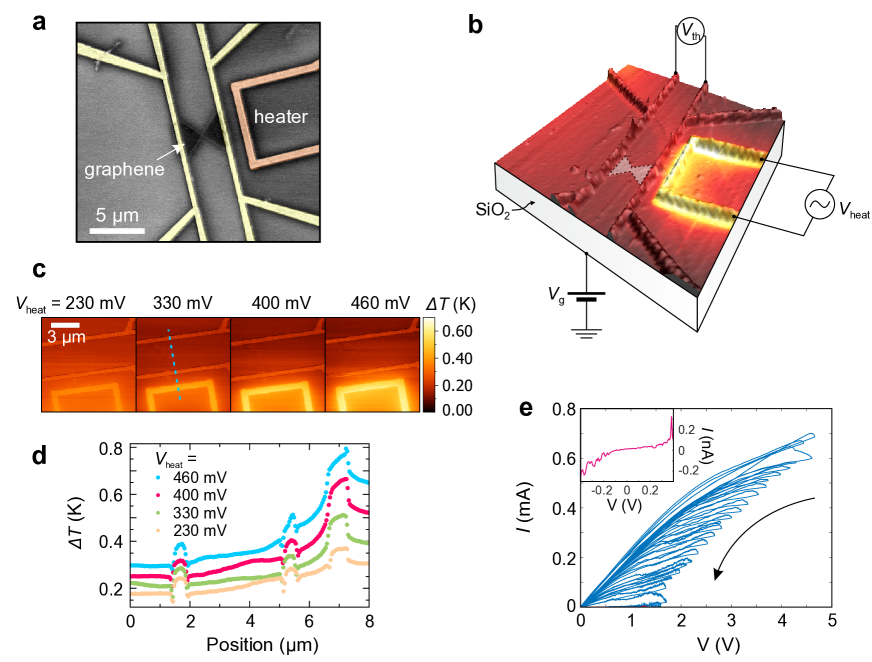
By passing a current through the micro-heater we create a temperature gradient across the junction3, 17, 18. We quantify this temperature gradient by cross-checking several methods to eliminate potential systematic errors. These are: (i) measuring the resistance of the left and right gold contacts; (ii) using COMSOL finite-element simulations; and (iii) using Scanning Thermal Microscopy (SThM) measurements. Using method (i) we measure a temperature difference between the hot (closer to the micro-heater) and cold (further from the micro-heater) contact as a function of heater power K W-1 at K (see Chapter 1 and 8 Supporting Information for details of the calibration method and an estimation of the total uncertainty, respectively). This is in close agreement with the finite-element simulations (method (ii)) which predict K W-1 and a constant temperature gradient K m-1 W-1 across the length of the graphene junction (see Figure S5). Figure 1b shows a temperature map overlaid onto a height profile that were simultaneously recorded using a SThM (method (iii)). From the temperature maps recorded for different heater powers in Figure 1c and d we extract a power-dependent temperature gradient K m-1 W-1 and a temperature difference K W-1 between the two gold contacts under ambient conditions and K W-1 for 77 K and vacuum (see Chapter 3 Supporting Information). For all the analysis presented below we will use the value extracted using method (i).
We use feedback-controlled electroburning19, 20, 21, 22 (see Figure 1e) to first form graphene nano-gaps suitable for characterisation of single molecules23 in which we subsequently couple C60 molecules functionalised with pyrene anchor groups (see Figure 2a). We have chosen this molecule since it is stable in air, has previously been successfully coupled to graphene electrodes24, and because its thermoelectric properties have been studied using various other techniques, including STM based break junctions12, 8 and electromigrated gold break junctions7. After electroburning we characterise the graphene gaps by measuring the current as a function of gate and bias voltage (stability diagram) at K in vacuum. Empty devices, where there are no carbon islands or ribbons bridging the gap, are characterised by non-linear curves and little or no gate modulation. After this first characterisation step we warm up the device and deposit C60 molecules by immersing the sample in a 10 M chloroform solution containing the C60 bisadducts for 1 min followed by blow drying with nitrogen gas. We then measured the devices again at low temperature to look for signatures of molecules. In total we fabricated 1080 two-terminal devices on which we performed feedback controlled electroburning. Due to limitations of our setup we were then only able to study 100 devices at low temperatures of which 16 devices showed signatures of molecule deposition: 1) a clear change from “empty” to Coulomb blockade after molecule deposition; 2) vibrational fingerprints in the excited state spectrum measured in the sequential tunneling regime.
Results and discussion
We often observe multiple overlapping, non-closing Coulomb diamonds which indicate the formation of molecular junctions where more than one molecule contribute to the electrical transport. In the following we discuss the data for 3 selected devices where the Coulomb diamonds close in the accessible back-gate region with addition energies meV. We focus on these devices as their transport is most likely dominated by a single molecule. Moreover, the large addition energies enables us to study well isolated energy levels that are expected to show the largest Seebeck coefficient. Chapter 5 of the Supporting Information includes the data of all measured devices.
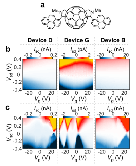
Figure 2b shows the stability diagrams of devices B, D and G measured at 77 K before and after molecule deposition. In Figure 2b, before molecule deposition, the source-drain current shows only weak gate dependence, but in Figure 2c regions of Coulomb blockade can be observed after deposition. We attribute the sequential electron tunneling after molecule deposition to the formation of a molecular junction.19, 24, 23. To further investigate the single electron transport, we studied several devices at low temperatures ( K). In a previous study we observed exited state lines in the sequential tunneling regime that correspond to and Raman active vibrational modes of C60 as well as centre-of-mass motion of the C60 molecule with respect to the graphene electrodes.24. In total, 7 of 16 devices showed similar evidence for vibrational excited states (see Table S2 Supporting Information). 4 out of 16 devices changed permanently to a non-conducting state after cool down to K and no low-temperature data could be recorded. The visibility of vibrational excited states strongly depends on temperature, the tunnel coupling to the leads25 and the Franck-Condon factors26, 27 which can vary drastically between different molecular junctions and the charge-transition investigated.28, 24 Moreover, density of states fluctuations in the graphene leads can lead to features inside the sequential tunneling regime, which do not run parallel to the edges of the Coulomb diamonds, that can obscure any vibrational fingerprint.29
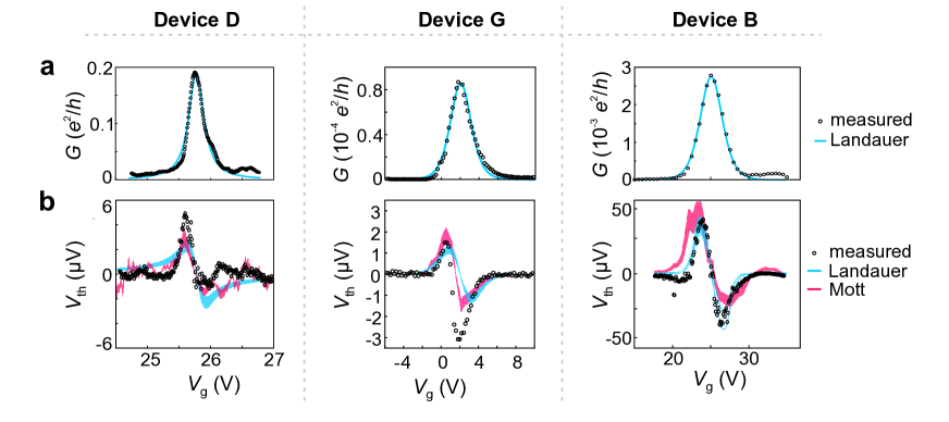
Next, we measure the gate dependent thermoelectric properties of the C60-graphene junctions. We apply an AC-voltage with modulation frequency to the micro-heater and measure the thermo-voltage drop on the device at a frequency for different back gate voltages (see Figure 1b).17 We focus on the high-conductance gate region around the Coulomb peaks (see gate traces in Figure 3a) since the thermo-voltage signal inside the Coulomb blocked region is smaller than the noise level of our measurement setup. Figure 3b shows the measured gate-depended thermo-voltage signal for Device D, G and B, recorded at mK, mK and mK, respectively. An increase of followed by a sign change, further decrease and subsequent increase towards zero can be observed. Similar results have been observed for 7 other devices (see Chapter 5 Supporting Information). Using the applied temperature bias we find maximum Seebeck coefficients ranging from 1.5 to 460 V K-1 (see Table 1). On average, these values are more than one order of magnitude larger than the Seebeck coefficients found in STM break junction experiments of C60 contacted with different metal electrodes12, 8. In the following we use a simple model for an isolated Breit-Wigner resonance to explain these results.
In the linear temperature and bias regime the conductance can be expressed in terms of the moments of the transmission coefficient as30
| (1) |
with
| (2) |
where we use the non-normalised probability distribution31
| (3) |
For a single, well isolated molecular level we can assume a Breit-Wigner resonance to describe the transmission probability :
| (4) |
where is the energy of the transport resonance, , are the tunnel couplings to the leads, and the lever arm is determined by the capacitive coupling of the molecule to the gate, source and drain electrodes32. The derivative of the Fermi-Dirac distribution is
| (5) |
In the limit where Equation (1) reduces to , and the tunnel coupling to the two leads can be inferred from the height and width of the Coulomb peak. In the opposite limit where the maximum conductance is proportional to while the width of the Coulomb peak is proportional to .
| Device name | (eV) | (meV/V) | (meV) | (V/K) | () | ( | (K) | |
| B | 88 | – | 9 | 221 | 220 | 0.003 | 0.01 | 77 |
| C | – | 10 | 188 | 140 | 0.08 | 0.08 | 77 | |
| D | 15 | 13 | 335 | 27 | 0.2 | 0.14 | 3.2 | |
| E | 16 | – | 6 | 53 | 238 | 0.006 | 0.02 | 11 |
| F | – | 11 | 84 | 460 | 0.01 | 0.11 | 77 | |
| G | 2 | – | 9 | 12 | 30 | 0.04 | 77 | |
| Q | 62 | 564 | 1.5 | 77 |
When a temperature bias is applied to a junction, the Fermi-Dirac distribution of the hot contact broadens compared to that of the cold contact. This gives rise to a thermal current , which leads to a thermo-voltage when measured under open circuit conditions . The ratio of the thermo-voltage and the temperature drop is the Seebeck coefficient . Similar to the conductance, the Seebeck coefficient is given by a Landauer-type expression using Equation 2, 3 and 5:
| (6) |
If varies only slowly with on the scale of , i.e. , then takes the well-known form of the Mott approximation33
| (7) |
In Figure 3b we compare our experimental results to the calculated thermo-voltages using the Mott approximation (equation 7) and the Landauer-type approach (equation 6), respectively, where the width of the curve indicates the error in estimating the temperature drop on the junction (see full error analysis in Chapter 8 Supporting Information). For both calculations the thermo-voltage was corrected by a damping factor due to the input impedance of the voltage amplifier (see Chapter 8.4 Supporting Information)5. To compare the measured thermo-voltage to that obtained from Equation 6 and 7 we assume that the temperature difference between the hot and the cold side of the molecule is equal to the temperature difference measured between the two gold contacts. Since cooling lengths of up to m have been reported for graphene34, the assumption that hot electrons injected from the gold contacts into the graphene leads do not thermalise before they reach the junction area approximately 1.7 m away from the gold contacts is justified. By assuming that no temperature drops on the graphene leads we only estimate a lower bound of . In addition, we neglect the effect of thermo-voltages created in the strongly p-doped graphene leads whose Seebeck coefficient is on the order of 10 17. However, this would result in a small, constant offset of the thermo-voltage in the applied gate voltage regime far away from the Dirac point of our graphene,22 which we do not observe in our experiments.
For the calculation of the Seebeck coefficient using the Landauer-type approach (equation 6) we estimate by equation 4 and extract the tunnel coupling by fitting the gate-dependent conductance traces to Equation 1 if . For those devices where , we estimate by fitting the conductance data with a thermally broadened conductance peak with ,35 where we fix K, and find a lower bound for by taking such that . Despite the fact that we can not uniquely determine in this regime, there is still good agreement between the measured and calculated thermo-voltage curves. This is due to the relative insensitivity of on the lifetime of the transport resonance when (see Figure S22).
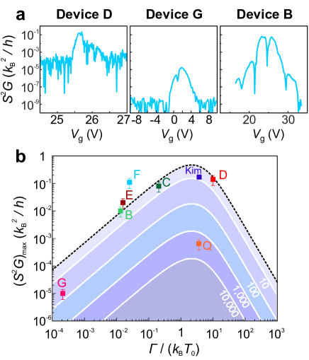
Finally, we use our experimental results to calculate the power factor for Devices D, G and B (see Figure 4a and Chapter 5 Supporting Information for other devices). Significantly, we find that can be tuned by several orders of magnitude by electrical gating to maximum values of (see Table 1). These values are one to two orders of magnitude larger than values found in C60 junctions without sufficient electric field control12, 8, 14 and comparable to the value found for C60 measured using gold break junctions with an electrical back gate7.
To evaluate the thermoelectric performance of different devices, we plot the maximum power factor on a log-log scale as a function of the temperature-normalized tunnel rate . We compare these values to the theoretical maximum calculated using
| (8) |
and Equations 1 - 6. In addition to the theoretical maximum power factor for devices with symmetric tunnel coupling (black dashed line), we plot the theoretical values for for different ratios between the fast and slow tunnel rates (solid white lines), where and . For devices in the regime where we use the lower bound as described above. Since the maximum power factor in this regime is independent of the asymmetry between the fast and slow tunnel coupling (see Figure S21), the measured power factor for these devices are expected to fall on the black dashed line corresponding to . For the device where G, B, E, F and C, we observe an increase of with increasing due to the power factor being proportional to . As approaches the power factor reaches a maximum for . Devices D and Q were measured close to this maximum, as was the C60 molecule measured by Kim et al. at 100 K denoted ‘Kim’ in Figure 4b.7 While devices D and ‘Kim’ have a power factor close to the theoretical limit, for device Q is several orders of magnitude lower as a result of the asymmetric coupling in this device. For the maximum power factor is expected to decrease with increasing as the lifetime broadening reduces the Seebeck coefficient. No devices where measured in this regime.
Based on our finding, we conclude that there are three desiderata for achieving high thermoelectric performance in molecular nanodevices. First, the molecular energy levels need to align closely with the Fermi level of the electrodes since the Seebeck coefficient is maximum for close to the centre of the transmission resonance. Second, the tunnel coupling needs to be such that the lifetime of the transmission resonance is comparable to at the operating temperature. Third, the tunnel couplings to the left and right electrode need to be equal to achieve a maximum power factor.
To summarise, we have fabricated thermoelectric nanodevices in which fullerene molecules are anchored between graphene source and drain leads. We demonstrate that by applying a thermal bias across the junction we can measure a gate dependent thermoelectricity. Our results show that by carefully tuning the transmission of a molecular junction towards sharp isolated resonance features, high power factors can be achieved approaching the theoretical limit of a thermally and lifetime broadened Coulomb peak. These results are relevant for the development of organic thermoelectric materials and our approach could also be applied to test hypotheses about the thermoelectric properties of molecules exhibiting quantum interference effects30 and spin caloritronics36.
Methods
Device fabrication
Our devices are fabricated from single-layer CVD-grown graphene, which we transfer onto a Si/300 nm SiO2 wafer with prepatterned 10 nm Cr/70 nm Au contacts and microheater. We pattern the graphene into a bow-tie shape (see Figure 1a) using standard electron beam lithography and O2 plasma etching. The channel length of the devices and the width of the narrowest part of the constriction are 3.5 m and 200 nm, respectively. To narrow down the constriction or form a nanogap we use a feedback-controlled electroburning technique in air22 using an ADWin Gold II card with a 30 kHz sampling rate. Electroburning cycles are repeated until a critical resistance of 500 M is reached.
Scanning thermal microscopy temperature measurements
This method uses a temperature sensitive calibrated microfabricated probe with an apex of a few tens of nm that is brought in direct solid-solid contact with the sample. The SThM response is a linear function of the local sample temperature . For a flat sample surface and constant tip-surface thermal resistance (that is the case when the tip is in contact with the same material – e.g. SiO2) it allows to directly map a 2D distribution of the temperature increase in the vicinity of the micro-heater , as well as to obtain an absolute value of the sample temperature increase due to micro-heater actuation using the following two quantitative methods: 1) In the “null-method” the probe apex temperature is varied, as the probe is brought repeatedly into contact with the sample. The value at which no change in the probe response occurs corresponds to , which provides an absolute temperature measurement with an error of about 15 % (see Chapter 2 and 3 Supporting Information for details). 2) In the SThM “addition” method the sample is heated both by the micro-heater as well as by the calibrated raise in the temperature of the sample stage, allowing to perform measurements under vacuum and variable sample temperatures (see Chapter 2 and 3 Supporting Information for more details). These measurements show good correlation of the experimentally measured temperature maps with the finite-elements models. SThM measurements under ambient conditions were performed using a commercial SPM (Bruker MultiMode with Nanoscope E controller) and a custom-built SThM modified AC Wheatstone bridge. A resistive SThM probe (Kelvin Nanotechnology, KNT-SThM-01a, 0.3 N/m spring constant, nm tip radius) served as one of the bridge resistors allowing precise monitoring of the probe AC electrical resistance at 91 kHz frequency via lock-in detection of the signal (SRS Instruments, SR830) as explained elsewhere37. Surface temperature maps were obtained at varying DC current to the probe that generated variable Joule heating of the probe tip. Several driving currents were used ranging from 0.10 to 0.40 mA leading to excess probe temperatures up to 34 K. The probe temperature - electrical resistance relation was determined employing a calibrated Peltier hot/cold plate (Torrey Pines Scientific, Echo Therm IC20) using a ratiometric approach (Agilent 34401A)37. The double-scan technique was used with different probe driving currents in order to obtain quantitative measurements of the surrounding and of the heater temperature38. Laser illumination on the probe (on the order of 5 K) added to the Joule heating and was accounted via measurement of corresponding probe resistance change. SThM thermal mapping was performed with a set-force below 15 nN during imaging to protect the tip and the sample from damage.
Electric and thermoelectric transport measurements
Graphene nano-structures were characterised in an Oxford Instruments Triton 200 dilution refrigerator with 20 mK base temperature. All measurements on C60 junctions were performed in a liquid nitrogen dip-stick setup. Electrical DC transport measurements were performed using low-noise DC electronics (Delft box). To measure the thermoelectric properties of nano-structures we used the method3. To this end an AC heater voltage with frequency was applied to the micro-heater using a HP33120a arbitrary waveform generator. The thermovoltage was measured with a SR560 voltage pre-amplifier and a SRS830 lock-in amplifier at a frequency (see Chapter 7 Supporting Information for more details).
Supporting Information Available
Calibration of the heater: Resistance method; Calibration of the heater: Scanning thermal microscopy; Calibration of the heater: Vacuum and variable temperature Scanning thermal microscopy; Calibration of the heater: COMSOL simulations; Supporting thermoelectric data: C60 junctions; Maximum power factor; Details on thermovoltage measurements; Error analysis.
Acknowledgements
We thank the Royal Society for a University Research Fellowship for J.H.W. This work is supported by the UK EPSRC (grant nos. EP/K001507/1, EP/J014753/1, EP/H035818/1, EP/K030108/1, EP/J015067/1 and EP/N017188/1). O.K. acknowledges EU QUANTIHEAT FP7 no 604668 and EPSRC EP/G015570/1 for funding instrumentation in Lancaster. P.G. thanks Linacre College for a JRF. This project/publication was made possible through the support of a grant from Templeton World Charity Foundation. The opinions expressed in this publication are those of the author(s) and do not necessarily reflect the views of Templeton World Charity Foundation. The authors would like to thank J. Sowa, H. Sadeghi and C. Lambert for helpful discussions.
Competing financial interests
The authors declare no competing financial interests.
References and Notes
- Heremans et al. 2013 Heremans, J. P.; Dresselhaus, M. S.; Bell, L. E.; Morelli, D. T. Nat. Nanotechnol. 2013, 8, 471–473.
- Venkatasubramanian et al. 2001 Venkatasubramanian, R.; Siivola, E.; Colpitts, T.; O’Quinn, B. Nature 2001, 413, 597–602.
- Small et al. 2003 Small, J. P.; Perez, K. M.; Kim, P. Phys. Rev. Lett. 2003, 91, 256801.
- Staring et al. 1993 Staring, A. A. M.; Molenkamp, L. W.; Alphenaar, B. W.; van Houten, H.; Buyk, O. J. A.; Mabesoone, M. A. A.; Beenakker, C. W. J.; Foxon, C. T. Europhys. Lett. 1993, 22, 57–62.
- Svensson et al. 2013 Svensson, S. F.; Hoffmann, E. A.; Nakpathomkun, N.; Wu, P. M.; Xu, H. Q.; Nilsson, H. A.; Sánchez, D.; Kashcheyevs, V.; Linke, H. New J. Phys. 2013, 15, 105011.
- Svensson et al. 2013 Svensson, S. F.; Hoffmann, E. A.; Nakpathomkun, N. New J. Phys. 2013, 15, 105011.
- Kim et al. 2014 Kim, Y.; Jeong, W.; Kim, K.; Lee, W.; Reddy, P. Nat. Nanotechnol. 2014, 9, 881–885.
- Evangeli et al. 2013 Evangeli, C.; Gillemot, K.; Leary, E.; Gonza, M. T.; Rubio-bollinger, G.; Lambert, C. J. Nano Lett. 2013, 13, 2141–2145.
- Reddy et al. 2007 Reddy, P.; Jang, S.-Y.; Segalman, R. A.; Majumdar, A. Science 2007, 315, 1568–1571.
- Baheti et al. 2008 Baheti, K.; Malen, J. A.; Doak, P.; Reddy, P.; Jang, S.-Y.; Tilley, T. D.; Majumdar, A.; Segalman, R. A. Nano Lett. 2008, 8, 715–719.
- Malen et al. 2009 Malen, J. A.; Doak, P.; Baheti, K.; Tilley, T. D.; Majumdar, A.; Segalman, R. A. Nano Lett. 2009, 9, 3406–3412.
- Yee et al. 2011 Yee, S. K.; Malen, J. A.; Majumdar, A.; Segalman, R. A. Nano Lett. 2011, 11, 4089–4094.
- Widawsky et al. 2012 Widawsky, J. R.; Darancet, P.; Neaton, J. B.; Venkataraman, L. Nano Lett. 2012, 12, 354–358.
- Rincon-Garcia et al. 2016 Rincon-Garcia, L.; Ismael, A. K.; Evangeli, C.; Grace, I.; Rubio-Bollinger, G.; Porfyrakis, K.; Agrait, N.; Lambert, C. J. Nat. Mater. 2016, 15, 289–293.
- Rincon-Garcia et al. 2016 Rincon-Garcia, L.; Evangeli, C.; Rubio-Bollinger, G.; Agrait, N. Chem. Soc. Rev. 2016, 45, 4285–4306.
- Lortscher 2013 Lortscher, E. Nat. Nanotechnol. 2013, 8, 381–384.
- Zuev et al. 2009 Zuev, Y. M.; Chang, W.; Kim, P. Phys. Rev. Lett. 2009, 096807, 1–4.
- Devender et al. 2016 Devender,; Gehring, P.; Gaul, A.; Hoyer, A.; Vaklinova, K.; Mehta, R. J.; Burghard, M.; Borca-tasciuc, T.; Singh, D. J.; Kern, K. Adv. Mater. 2016, 28, 6436–6441.
- Prins et al. 2011 Prins, F.; Barreiro, A.; Ruitenberg, J. W.; Seldenthuis, J. S.; Vandersypen, L. M. K.; Zant, H. S. J. V. D. Nano Lett. 2011, 11, 4607–4611.
- Lau et al. 2014 Lau, C. S.; Mol, J. A.; Warner, J. H.; Briggs, G. A. D. Phys. Chem. Chem. Phys. 2014, 16, 20398–20401.
- Puczkarski et al. 2015 Puczkarski, P.; Gehring, P.; Lau, C. S.; Liu, J.; Ardavan, A.; Warner, J. H.; Briggs, G. A. D.; Mol, J. A. Appl. Phys. Lett. 2015, 107, 133105.
- Gehring et al. 2016 Gehring, P.; Sadeghi, H.; Sangtarash, S.; Lau, C. S.; Liu, J.; Ardavan, A.; Warner, J. H.; Lambert, C. J.; Briggs, G. A. D.; Mol, J. A. Nano Lett. 2016, 16, 4210–4216.
- Mol et al. 2015 Mol, J. A.; Lau, C. S.; Lewis, W. J. M.; Sadeghi, H.; Roche, C.; Cnossen, A.; Warner, J. H.; Lambert, C. J.; Anderson, H. L.; Briggs, G. A. D. Nanoscale 2015, 7, 13181–13185.
- Lau et al. 2016 Lau, C. S.; Sadeghi, H.; Rogers, G.; Sangtarash, S.; Dallas, P.; Porfyrakis, K.; Warner, J.; Lambert, C. J.; Briggs, G. A. D.; Mol, J. A. Nano Lett. 2016, 16, 170–176.
- Schinabeck et al. 2016 Schinabeck, C.; Erpenbeck, A.; Härtle, R.; Thoss, M. Phys. Rev. B 2016, 94, 201407.
- Park et al. 2000 Park, H.; Park, J.; Lim, A. K. L.; Anderson, E. H.; Alivisatos, A. P.; McEuen, P. L. Nature 2000, 407, 57–60.
- Burzuri et al. 2014 Burzuri, E.; Yamamoto, Y.; Warnock, M.; Zhong, X.; Park, K.; Cornia, A.; van der Zant, H. S. J. Nano Lett. 2014, 14, 3191–3196.
- de Leon et al. 2008 de Leon, N. P.; Liang, W.; Gu, Q.; Park, H. Nano Lett. 2008, 8, 2963–2967.
- Gehring et al. 2017 Gehring, P.; Sowa, J.; Cremers, J.; Wu, Q.; Sadeghi, H.; Warner, J. H.; Lambert, C. J.; Anderson, H. L.; Briggs, G. A. D.; Mol, J. A. ACS Nano 2017, 11, 5325–5331.
- Finch and Lambert 2009 Finch, C. M.; Lambert, C. J. Phys. Rev. B 2009, 79, 033405.
- Lambert 2015 Lambert, C. J. Chem. Soc. Rev. 2015, 44, 875–888.
- Hanson 2007 Hanson, R. Rev. Mod. Phys. 2007, 79, 1217–1265.
- Lunde and Flensberg 2005 Lunde, A. M.; Flensberg, K. J. Phys. Condens. Matter 2005, 17, 3879–3884.
- Song et al. 2011 Song, J. C. W.; Rudner, M. S.; Marcus, C. M.; Levitov, L. S. Nano Lett. 2011, 11, 4688–4692.
- Beenakker 1991 Beenakker, C. Phys. Rev. B 1991, 44, 1646–1656.
- Wang et al. 2010 Wang, R.-Q.; Sheng, L.; Shen, R.; Wang, B.; Xing, D. Y. Phys. Rev. Lett. 2010, 105, 057202.
- Tovee et al. 2012 Tovee, P.; Pumarol, M.; Zeze, D.; Kjoller, K.; Kolosov, O. J. Appl. Phys. 2012, 112, 114317.
- Menges et al. 2012 Menges, F.; Riel, H.; Stemmer, A.; Gotsmann, B. Nano Lett. 2012, 12, 596–601.