In situ high resolution real-time quantum efficiency imaging for photocathodes
Abstract
Aspects of the preparation process and performance degradation are two major problems of photocathodes. The lack of a means for dynamic quantum efficiency measurements results in the inability to observe the inhomogeneity of the cathode surface by fine structural analysis and in real time. Here we present a simple and scalable technique for in situ real-time quantum efficiency diagnosis. An incoherent light source provides uniform illumination on the cathode surface, and solenoid magnets are used as lens for focusing and imaging the emitted electron beam on a downstream scintillator screen, which converts the quantum efficiency information into fluorescence intensity distribution. The microscopic discontinuity and the dynamic changes of the quantum efficiency of a gallium arsenide photocathode are observed at a resolution of a few microns. An unexpected uneven decrease of the quantum efficiency is also recorded. The work demonstrates a new observation method for photoemission materials research.
- PACS numbers
-
85.60.Ha, 29.20.Ej
pacs:
Valid PACS appear hereOver the past several decades, photocathodes have played various important roles in many fields, such as image intensifier Biberman (2013), ultra-fast streak camera Kassier et al. (2010), and photomultiplier tube Engstrom (1980), etc. Especially in recent years, photocathodes have become the most important high-brightness electron sources to drive X-ray free electron lasers or Compton back-scattering -ray sources Dowell et al. (1993); Emma et al. (2010); Dowell et al. (2010); Dowell and Schmerge (2009); Akre et al. (2008); Ding et al. (2009); Zheng et al. (2016), which have promoted the development of optical sciences, biological sciences, organic chemistry and many other cutting-edge sciences Chapman (2009); Rohringer et al. (2012); Hirata et al. (2014); Suga et al. (2015).
Although photocathodes have been widely used, there are still some questions surrounding them, among which the microscopic dynamic process of their performance, which mostly refers to the quantum efficiency (QE), is the utmost importance. For example, the relationship between the photocathode QE degradation and the environment, such as temperature or ion back-bombardment, has been widely studied Fischer et al. (1994); Aulenbacher et al. (1997); Lewellen (2002); Qiang (2010); Zhang et al. (2011); Grames et al. (2011), but the details are mostly hypothetical or based on simulation. Also, field emission defects and the non-uniformity of photocathode’s surface will reduce the quality of the high-brightness electron beam and the X-ray or -ray sources driven by it, making laser transverse shaping fails to some extent, but it is complicated to measure the QE uniformity in the small range of the laser irradiation spot Pandey et al. (2009); Shao et al. (2016). In addition, the dynamic effect of each component on the cathode performance during the preparation or activation of the semiconductor photocathode is typically measured only by laser irradiation at a single spot. All these issues arise from the lack of a means for in situ high-resolution real-time QE observation. Earlier studies used a laser focused to a small spot to raster scan the QE of the cathode surface. This method is called ’QE mapping’, the resolution of which could reach m Grames et al. (2011); Gubeli et al. (2001); Sinclair et al. (2007); Cultrera et al. (2011); Zhou et al. (2012); Riddick et al. (2013); Filippetto et al. (2015), but the scanning time would last for minutes to hours, depending on the resolution. Photoemission electron microscopy (PEEM) could offer the best resolution ( nm) of QE distribution Anders et al. (1999); Polyakov et al. (2013). However, this technique requires the cathode to be moved into its system, thus the photocathodes cannot be observed in real-time or in situ.
In this paper, we present a simple in situ real-time QE imaging of a high-voltage photocathode DC gun, as well as some of the cathode dynamic changes observed during its use.
This study was conducted at the Tera-Hertz free electron laser (THz FEL) facility Wu et al. (2014) at the China Academy of Engineering Physics (CAEP). The electron beam line downstream the high-voltage DC gun was used as the imaging system, which is shown in Fig. 1(a). In order to avoid the coupling of the transverse distribution of the coherent light source, a lamp, as an incoherent light source, was placed far enough from the photocathode, to provide a uniform illumination. Although QE is a function of the wavelength, a uniform illumination ensures that the transverse density distribution of the emitted electrons is proportional to the relative QE distribution at any corresponding wavelength. The emitted electron beam was then accelerated by the electric field inside the high-voltage gun. The voltage can reach 320 kV, which makes the field gradient on the cathode surface 4.14 MV/m, as calculated by the SUPERFISH code Billen and Young (1993). In this work, four pieces of gallium arsenide (GaAs) photocathodes were tested. All the cathodes were flat, 18 cm in diameter and covered by a tantalum cap. The average emission current was about a pico to a nano Ampere, thus the space charge effect can be neglected, and it was a linear electron optical system. Two solenoids were placed downstream to provide two different images, one is an enlarged image with better resolution to give some specific local details, and the other image is smaller so as to observe the whole QE distribution over the cathode. The images are generated at the YAG phosphor screens and captured by the CCDs. A laser scanning system focuses the laser to a specific point and measures the QE at that point, making the absolute QE distribution of the entire cathode available.
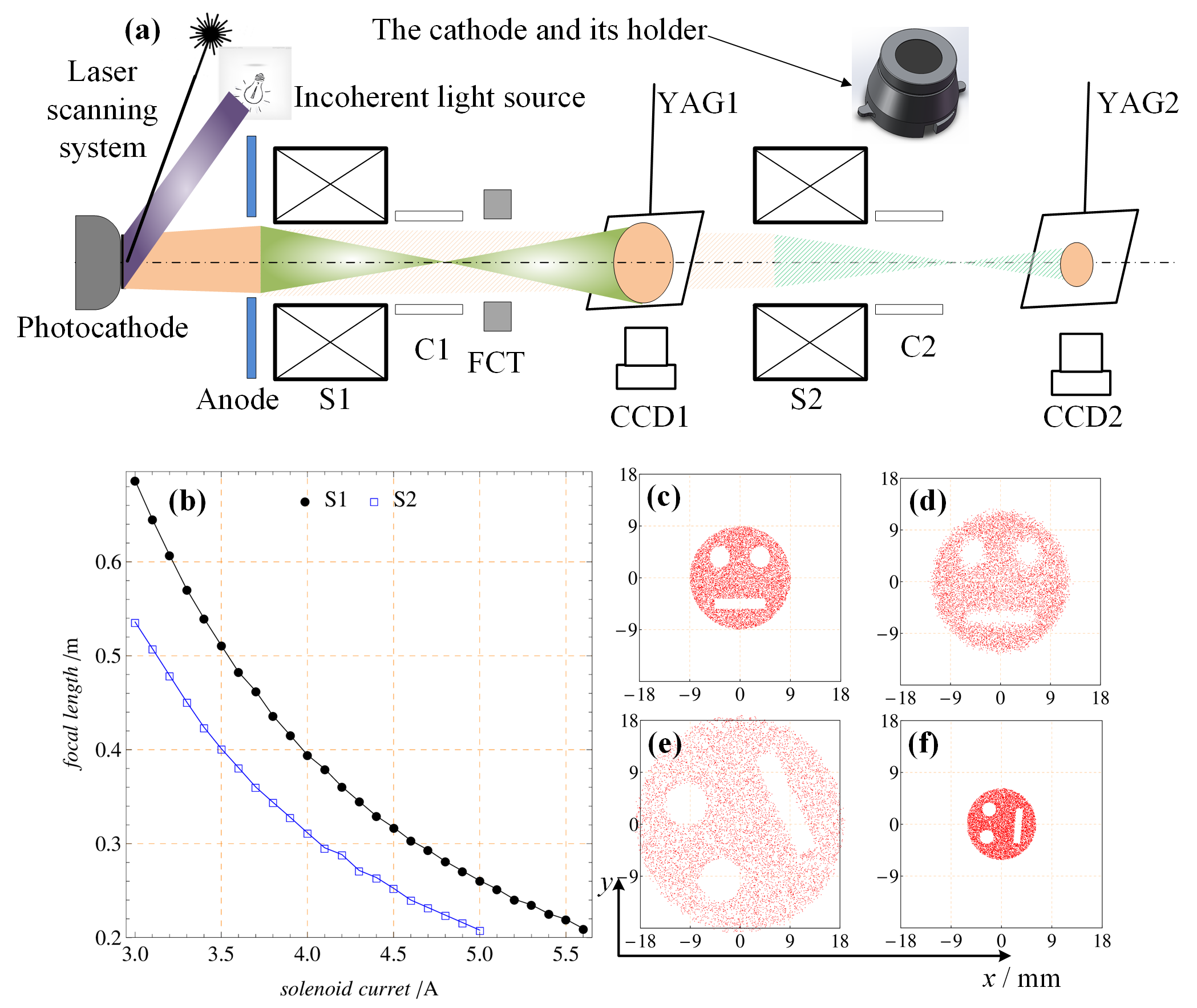
The equivalent focal length of the solenoids versus the excitation current, as simulated by the particle tracking code ASTRA Flöttmann (2011), is shown in Fig. 1(b). The beam was rotated when passing through the solenoid. An ’evil face’ pattern was used to simulate the magnification and rotation. In the simulation, macro-particles were generated by the code ASTRA with a uniform distribution and the same size as the photocathode, as shown in Fig. 1(c). Fig. 1(d) shows the electron distribution outside the gun with no solenoid magnet, where the pattern turned to be larger and not clear due to the initial transverse momentum. The enlarged pattern, with the excitation current of S1 at 5.7 A, is shown in Fig. 1(e). In this case, the image magnification was about 2.1, and the rotation was about 116∘ counterclockwise. When the current of S1 and S2 were 4.4 A and 4.0 A, respectively, a smaller image could be captured at YAG2, as shown in Fig. 1(f), where the magnification was about 0.6, and the rotation was 86∘ counterclockwise.
The transverse spatial resolution is mainly determined by the beamline optical magnification and the CCD resolution. The beamline optical magnification was limited by three factors, which are the vacuum pipe size ( 60 mm in diameter), the YAG screen size (25 mm wide and 18 mm high) and the maximum current of the power sources of S1 and S2 ( 6 A and 4 A, respectively). For all these factors the magnification was found to be less than 3.The CCD is a model ’FL3-GE-13S2M-C’ PointGrey camera poi (2013), equipped with a Nikon ’AF Nikkor 50mm f/1.8D’ lens. The best resolution of this CCD is about 30 m/pixel, making the best resolution of the whole QE imaging system be about 10 m/pixel. The dynamic range of the camera is 59.14 dB, which indicates that the imaging method can theoretically resolve QE differences as small as 10-6.
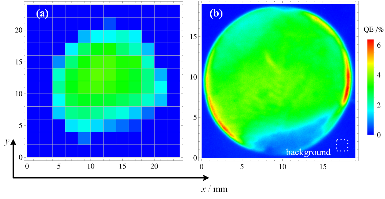
The results obtained by the two methods for measuring QE distribution of cathode #1 are shown in Fig. 2. For the former, the photo-injector drive laser was focused into a small spot to scan the QE with a step size of about 1.81 mm. The laser had an approximately round Gaussian transverse distribution with a root mean square (RMS) size of 0.64 mm. The space charge limit (SCL) was calculated as Rao and Dowell (2013): pC,where is the dielectric constant in the vacuum. It means the emitted bunch charge would be proportional to the QE, as long as it is less than 94 pC. The laser power could be continuously adjusted in the range from 0 to 8 W at the wavelength of 532 nm. And the duty factor was adjustable from 5 to 1. The raster scanning QE distribution is shown in Fig. 2(a). The largest single bunch charge is 50.2 pC, less than 94 pC.
For comparison, the pseudo-color picture of the QE distribution captured at YAG2 is shown in Fig. 2(b). As the saturation was not reached, the brightness of the phosphor screen was proportional to the charge density, which was also proportional to the QE distribution. The absolute value of the QE was given by a single spot of the scanning result in a relatively uniform region. The rotation of the image has been restored. Also, by cathode size calibration, the distance between two pixels represented about 82 m on the cathode surface. The image was sharper, and most importantly it took much less time. The captured bitmap (BMP) images have only 256 levels of grayscale, so the dynamic range of this system was about 24 dB. The selected background within the dotted white box has an averaged 3.95 level of grayscale, making the signal-to-noise ratio 65:1.
Neither of the two methods can obtain accurate results at the edge of the cathode. For the scanning method, the laser will be cut at the edge, thus the QE map is a little larger than the cathode in size. Meanwhile, for the imaging method, the lamp light is intensified by the tantalum cap, so the QE will be greater than the actual value at the edge. Both methods show that the lower right corner of the cathode has lower QE. These non-uniformities are due to the nonuniform growth of the Cs-O active layer on the GaAs cathode surface. The optimum number of atoms in the active layer is Cs:O 2:1 Clark (1975), but in the cathode preparation chamber, the two Cs sources are placed at both side of the cathode, one of which evaporates less than the other.
The dynamic process of the QE degradation caused by ion bombardment was observed in situ on the surface of cathode #1, as shown in Fig. 3. The electron gun was working in the continuous wave (CW) mode for about 2 hours to make the effect of the ion bombardment significant. The average current of the cathode emission was 0.5 mA. The laser struck near the center of the cathode. The average laser power was under 50 mW to make sure that the temperature at the laser spot on the cathode did not change greatly (less than 1 ∘C, simulated by Ansys code). The QE of the photocathode should be exponentially decreased if only the influence of vacuum was considered. Accordingly, the ratio of the original QE image (Fig. 1(b)) to the new QE image after this CW operation should be flat. But in reality it shows obvious differences, as shown in the red dashed circle and the blue dashed ellipse of Fig. 3(a).
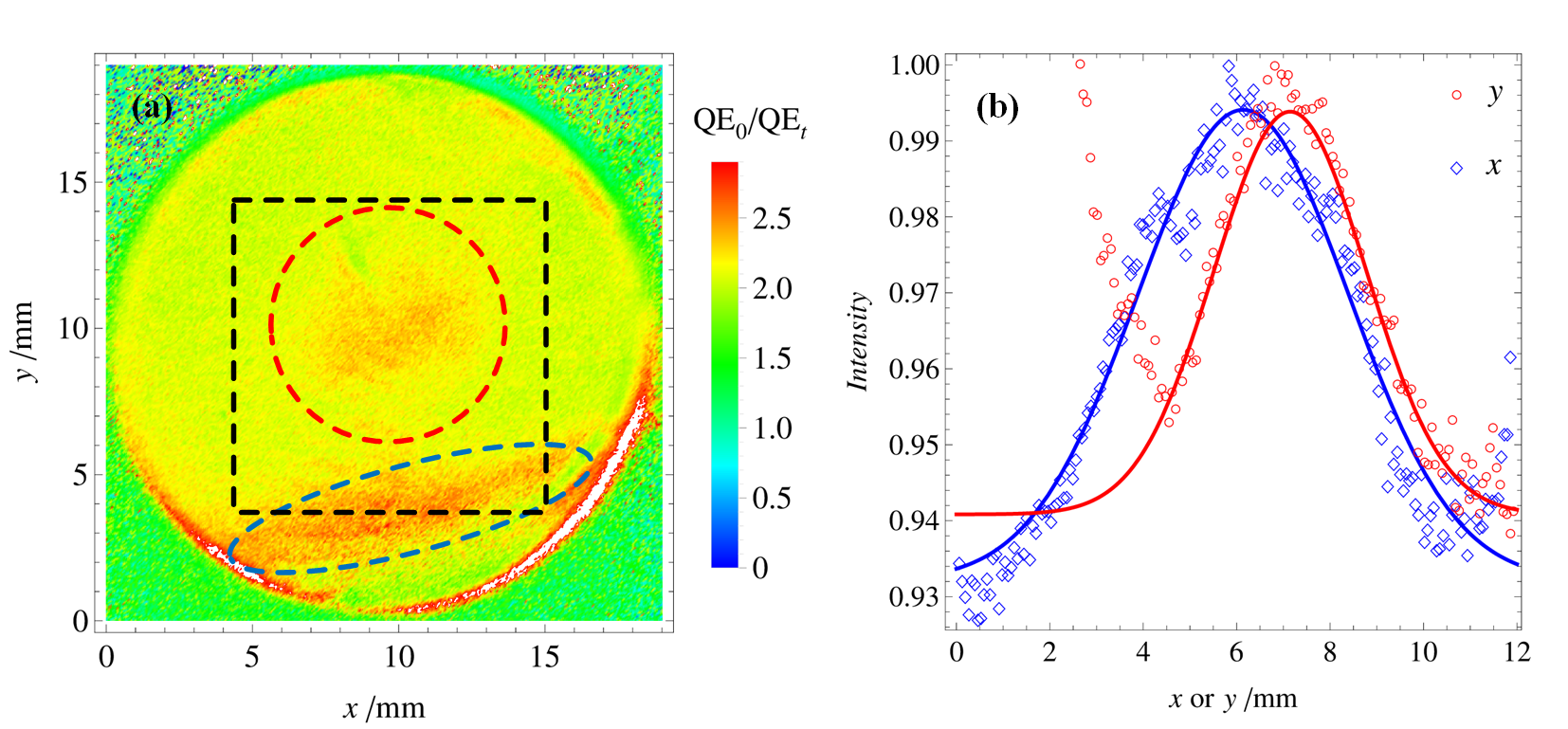
Since the cathode is flat and the electric field of the electron gun is radially symmetrical, the ions, produced by ionization in the vacuum system and accelerated by the electric field, would strike around the center, making the QE of that area degrade faster. The rate of decline, to some extent, represents the density of the ions. Therefore, the distribution within the red dashed circle represents the ion back-bombardment distribution and its effect on QE. The distribution projections in the and directions inside the black dashed square are shown in Fig. 3(b), which can be fitted as a Gaussian distribution. The results were similar to those obtained by the Monte Carlo simulation in the RF gun Qiang (2010).
It could also be observed that the QE near the lower edge of the photocathode decreased more rapidly than it did in other areas, as shown in the blue dashed ellipse in Fig. 3(a). This phenomenon is an evidence of different dark life-time related to different activation layers across the GaAs photocathode, which suggests a way of improving the preparation process to obtain uniform QE on the cathode surface. However, the areas above and below the ellipse had almost the same QE descending speed, which is worthy of further study.
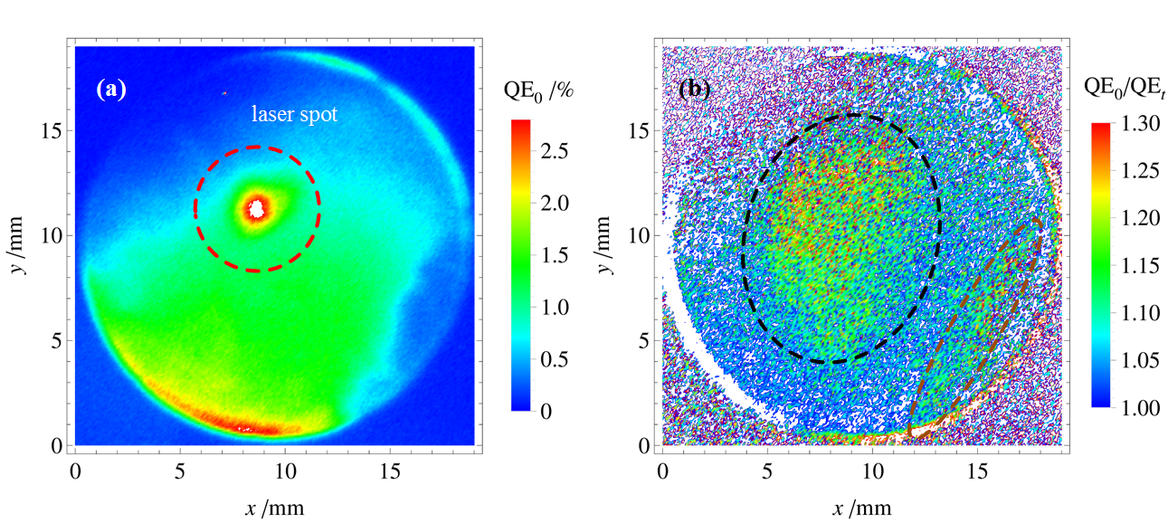
The QE degradation difference due to temperature difference was also studied. An image of photocathode #2 with more non-uniform QE distribution was captured By adjusting the laser to a very low average power, the emitted electron bunch generated by the laser irradiation would have a very small charge density. Therefore, the space charge effect could be ignored, and the laser distribution could be imaged together with the QE imaging, when the laser irradiates a relatively uniform region on the cathode. This would be an in situ laser transverse distribution imaging method. The laser RMS size of mm was measured in this way and the result was in good agreement with the one measured by the laser profile CCD. The laser spot location was within the red dashed circle in Fig. 4(a).
In order to avoid ion back-bombardment-induced QE degradation, the high-voltage of the DC gun was turned off, and no electrons were emitted from the cathode surface to generate ions. The laser was then operated in continuous mode to heat the cathode surface with a 1 W average power for 35 minutes. When the laser was striking the cathode, the vacuum inside the gun remained at about 3 Pa. The ratio of the original QE image to the new one after this CW operation was not flat ether. With the laser irradiation on the center, a large area showed a QE decrease of about 10% 30%, as shown in the black dashed ellipse in Fig. 4(b).
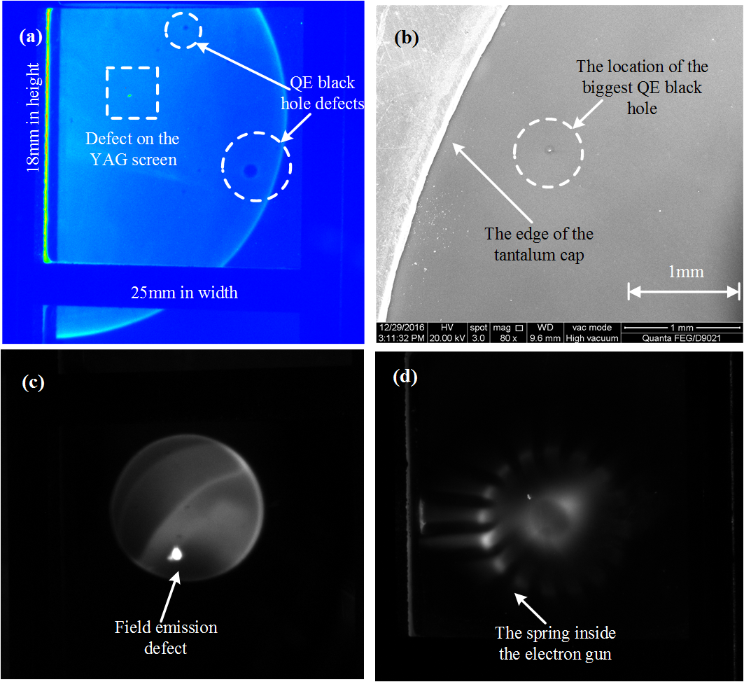
Some lower QE defects like a kind of ’black hole’ were observed on the enlarged QE image, as shown in Fig. 5(a). The activation current of S1 is 5.7 A, corresponding to an image magnification factor of about 2.1. The resolution of this image is about 36 m/pixel, making the resolution on the cathode surface about 17 m/pixel. The biggest ’black hole’ is about 391 m in diameter and the smallest one is about 34 m in diameter. These defects may cause the laser transverse shaping to fail to some extent. And the causes of these defects need further investigation.
These defects are also observed in the SEM images. The SEM image of the biggest defects is shown in Fig. 5(b), which is much smaller than that observed on the QE image. The in situ imaging can provide additional information obviously.
Additionally, some field emission defects were observed on the surface of cathode #4, as shown in Fig. 5(c). The QE distribution of cathode #4 exhibits a step-like shape, which might be caused by some preparation process errors. In addition, there was an obvious field emission defect below the center, which will lead to an increase in dark current. Marking the location and the strength of these field emission defects on the cathode surface will make it possible to find ways to clean them.
The linear optical system still works when the cathode is unloaded, and high-voltage breakdown could be observed when the gun was undergoing a high-voltage conditioning, as shown in Fig. 5(d). The spring structures of the cathode holder in the gun can be observed and it appears to be a good way to monitor the conditioning process.
Furthermore, the linear optical system can be designed inside the photocathode preparation chambers with a single solenoid and a YAG screen. In such a case, the changes of QE on the cathode surface can be captured in real-time during its fabrication and preparation.
In summary, an in situ high resolution real-time QE imaging system for photocathode was developed in the CAEP THz FEL beamline. The resolution of this system reached about 17 m/pixel and the dynamic range was about 24 dB. The dynamic processes of the QE degradation induced by the back-bombardment and temperature rising were observed separately. The defects of the lower QE and field emission were located and measured. Additionally, the breakdown of the gun conditioning could also be captured with this system. This work greatly extends the observing capability in measuring the photocathode performance during preparation and operation, and greatly expands the understanding of the photocathode QE degradation process and details of the preparation process, which in turn benefits researches in high-brightness electron sources, image intensifiers, photo-multipliers tubes and particles accelerators in general.
References
- Biberman (2013) L. Biberman, Photoelectronic Imaging Devices: Physical processes and methods of analysis, Vol. 1 (Springer Science & Business Media, 2013).
- Kassier et al. (2010) G. H. Kassier, K. Haupt, N. Erasmus, E. Rohwer, H. Von Bergmann, H. Schwoerer, S. M. Coelho, and F. D. Auret, Review of Scientific Instruments 81, 105103 (2010).
- Engstrom (1980) R. W. Engstrom, Photomultiplier handbook (RCA Corp., 1980).
- Dowell et al. (1993) D. Dowell, K. Davis, K. Friddell, E. Tyson, C. Lancaster, L. Milliman, R. Rodenburg, T. Aas, M. Bemes, S. Bethel, et al., Applied physics letters 63, 2035 (1993).
- Emma et al. (2010) P. Emma, R. Akre, J. Arthur, R. Bionta, C. Bostedt, J. Bozek, A. Brachmann, P. Bucksbaum, R. Coffee, F.-J. Decker, et al., Nature Photonics 4, 641 (2010).
- Dowell et al. (2010) D. Dowell, I. Bazarov, B. Dunham, K. Harkay, C. Hernandez-Garcia, R. Legg, H. Padmore, T. Rao, J. Smedley, and W. Wan, Nuclear Instruments and Methods in Physics Research Section A: Accelerators, Spectrometers, Detectors and Associated Equipment 622, 685 (2010).
- Dowell and Schmerge (2009) D. H. Dowell and J. F. Schmerge, Physical Review Special Topics - Accelerators and Beams 12, 074201 (2009).
- Akre et al. (2008) R. Akre, D. Dowell, P. Emma, J. Frisch, S. Gilevich, G. Hays, P. Hering, R. Iverson, C. Limborg-Deprey, H. Loos, A. Miahnahri, J. Schmerge, J. Turner, J. Welch, W. White, and J. Wu, Phys. Rev. ST Accel. Beams 11, 030703 (2008).
- Ding et al. (2009) Y. Ding, A. Brachmann, F.-J. Decker, D. Dowell, P. Emma, J. Frisch, S. Gilevich, G. Hays, P. Hering, Z. Huang, et al., Physical review letters 102, 254801 (2009).
- Zheng et al. (2016) L. Zheng, Y. Du, Z. Zhang, H. Qian, L. Yan, J. Shi, Z. Zhang, Z. Zhou, X. Wu, X. Su, D. Wang, Q. Tian, W. Huang, H. Chen, and C. Tang, Nuclear Instruments and Methods in Physics Research Section A: Accelerators, Spectrometers, Detectors and Associated Equipment 834, 98 (2016).
- Chapman (2009) H. N. Chapman, Nature materials 8, 299 (2009).
- Rohringer et al. (2012) N. Rohringer, D. Ryan, R. A. London, M. Purvis, F. Albert, J. Dunn, J. D. Bozek, C. Bostedt, A. Graf, R. Hill, et al., Nature 481, 488 (2012).
- Hirata et al. (2014) K. Hirata, K. Shinzawa-Itoh, N. Yano, S. Takemura, K. Kato, M. Hatanaka, K. Muramoto, T. Kawahara, T. Tsukihara, E. Yamashita, et al., Nature methods 11, 734 (2014).
- Suga et al. (2015) M. Suga, F. Akita, K. Hirata, G. Ueno, H. Murakami, Y. Nakajima, T. Shimizu, K. Yamashita, M. Yamamoto, H. Ago, et al., Nature 517, 99 (2015).
- Fischer et al. (1994) H. Fischer, P. Drescher, and E. Reichert, in Photocathodes for Polarized Electron Sources for Accelerators (1994) pp. 249–260.
- Aulenbacher et al. (1997) K. Aulenbacher, C. Nachtigall, H. Andresen, J. Bermuth, T. Dombo, P. Drescher, H. Euteneuer, H. Fischer, D. Harrach, P. Hartmann, J. Hoffmann, P. Jennewein, K. Kaiser, S. K枚bis, H. Kreidel, J. Langbein, M. Petri, S. Pl眉tzer, E. Reichert, M. Schemies, H.-J. Sch枚pe, K.-H. Steffens, M. Steigerwald, H. Trautner, and T. Weis, Nuclear Instruments and Methods in Physics Research Section A: Accelerators, Spectrometers, Detectors and Associated Equipment 391, 498 (1997).
- Lewellen (2002) J. W. Lewellen, Physical Review Special Topics-Accelerators and Beams 5, 020101 (2002).
- Qiang (2010) J. Qiang, Nuclear Instruments and Methods in Physics Research Section A: Accelerators, Spectrometers, Detectors and Associated Equipment 614, 1 (2010).
- Zhang et al. (2011) S. Zhang, S. Benson, and C. H-Garcia, Nuclear Instruments and Methods in Physics Research Section A: Accelerators, Spectrometers, Detectors and Associated Equipment 631, 22 (2011).
- Grames et al. (2011) J. Grames, R. Suleiman, P. Adderley, J. Clark, J. Hansknecht, D. Machie, M. Poelker, and M. Stutzman, Physical Review Special Topics-Accelerators and Beams 14, 043501 (2011).
- Pandey et al. (2009) A. D. Pandey, G. Müller, D. Reschke, and X. Singer, Physical Review Special Topics-Accelerators and Beams 12, 023501 (2009).
- Shao et al. (2016) J. Shao, J. Shi, S. P. Antipov, S. V. Baryshev, H. Chen, M. Conde, W. Gai, G. Ha, C. Jing, F. Wang, et al., Physical review letters 117, 084801 (2016).
- Gubeli et al. (2001) J. Gubeli, R. Evans, A. Grippo, K. Jordan, M. Shinn, and T. Siggins, Nuclear Instruments and Methods in Physics Research Section A: Accelerators, Spectrometers, Detectors and Associated Equipment 475, 554 (2001).
- Sinclair et al. (2007) C. Sinclair, P. Adderley, B. Dunham, J. Hansknecht, P. Hartmann, M. Poelker, J. Price, P. Rutt, W. Schneider, and M. Steigerwald, Physical Review Special Topics-Accelerators and Beams 10, 023501 (2007).
- Cultrera et al. (2011) L. Cultrera, I. Bazarov, A. Bartnik, B. Dunham, S. Karkare, R. Merluzzi, and M. Nichols, Applied Physics Letters 99, 152110 (2011).
- Zhou et al. (2012) F. Zhou, A. Brachmann, F.-J. Decker, P. Emma, S. Gilevich, R. Iverson, P. Stefan, and J. Turner, Phys. Rev. ST Accel. Beams 15, 090703 (2012).
- Riddick et al. (2013) B. Riddick, E. Montgomery, R. Fiorito, H. Zhang, A. Shkvarunets, Z. Pan, and S. Khan, Physical Review Special Topics-Accelerators and Beams 16, 062802 (2013).
- Filippetto et al. (2015) D. Filippetto, H. Qian, and F. Sannibale, Applied Physics Letters 107, 042104 (2015).
- Anders et al. (1999) S. Anders, H. A. Padmore, R. M. Duarte, T. Renner, T. Stammler, A. Scholl, M. R. Scheinfein, J. Stöhr, L. Séve, and B. Sinkovic, Review of Scientific Instruments 70, 3973 (1999).
- Polyakov et al. (2013) A. Polyakov, C. Senft, K. F. Thompson, J. Feng, S. Cabrini, P. J. Schuck, H. A. Padmore, S. J. Peppernick, and W. P. Hess, Phys. Rev. Lett. 110, 076802 (2013).
- Wu et al. (2014) D. Wu, Q. Pan, K. Li, D. Xiao, R. Yang, H. Wang, X. Yang, and M. Li, in Proceedings of SAP2014, LanZhou, China (2014) pp. 12–15.
- Billen and Young (1993) J. H. Billen and L. M. Young, in Particle Accelerator Conference, 1993., Proceedings of the 1993 (IEEE, 1993) pp. 790–792.
- Flöttmann (2011) K. Flöttmann, ASTRA: A space charge tracking algorithm (2011).
- poi (2013) Flea3 GE Technical Reference Manual, Point Grey Research Inc (2013).
- Rao and Dowell (2013) T. Rao and D. H. Dowell, An engineering guide to photoinjectors (CreateSpace Independent Publishing Platform, 2013).
- Clark (1975) M. G. Clark, Journal of Physics D: Applied Physics 8, 535 (1975).