A Multi-Bit Neuromorphic Weight Cell using Ferroelectric FETs, suitable for SoC Integration
Abstract
A multi-bit digital weight cell for high-performance, inference-only non-GPU-like neuromorphic accelerators is presented. The cell is designed with simplicity of peripheral circuitry in mind. Non-volatile storage of weights which eliminates the need for DRAM access is based on FeFETs and is purely digital. The Multiply-and-Accumulate operation is performed using passive resistors, gated by FeFETs. The resulting weight cell offers a high degree of linearity and a large ON/OFF ratio. The key performance tradeoffs are investigated, and the device requirements are elucidated.
Index Terms:
Neuromorphic, FeFET, DNNI Introduction
Hardware accelerators for Deep Neural Nets (DNNs) are receiving increased attention as Neural Network-based applications proliferate. Currently, hardware accelerators fall into two categories: GPU-like devices [1] with reduced-precision arithmetic (and possibly an improved memory access architecture), and more ”literal” implementations of DNNs as sets of resistive cross-bar arrays ([2, 3, 4, 5, 6]). While the former approach is already seeing practical use, the latter is still in the research phase. The key characteristics of the ”literal” approach are local storage of network weights and analog computation of the outputs as linear combinations of inputs. By storing network weights locally, the time and energy required to copy them from off-chip DRAM is eliminated. The specific array architectures, weight cells, and even details of operation are still being investigated and vary considerably across implementations. One of the key design decisions is whether to support on-chip training ([1, 2, 5]), or whether weights are to be transferred to the chip after off-line training [7]. Each approach has advantages and disadvantages. On-chip training offers the most local customizability, as well as a near-complete suppression of the impact of process variability (since the training is done for the specific hardware). The key disadvantages are the significantly increased complexity of the peripheral circuitry needed to support on-chip backpropagation, as well as the much higher required precision of the weights (to handle the many small increments in the weights during the iterative training process). Implementations with off-chip training are more straightforward to program, but must contend with process variability impacting weight values and imperfect programming [7]. It should be noted that off-chip training with analog or multi-bit digital weights which are implemented as multiple states of a single device suffers from similar programming complexity as on-chip programming. Due to the non-linearity of the response of all standard NVMs, the number or duration of programming pulses to achieve a desired weight depends on the current state of the weight ([2, 7]). A sense-program iteration is therefore required to achieve the desired weight, even though the value for the target weight was computed off-line.
In this paper, the assumption is made that near-term applications for neuromorphic accelerators on mobile SoCs will not benefit from on-chip training, which is instead relegated to the cloud. The focus is on improved inference performance and power reduction. The cross-bar array and non-volatile weight cells are designed for programming simplicity and robustness w.r.t. process and programmation variability, enabling effective transfer of off-line weights. No iterative programming is required. Additionally, all training is assumed to be centralized (with possibly crowd-sourced data).
In order to achieve reasonable immunity to process variability and programmation errors, a multi-bit digital representation of weights is used. It has been demonstrated (in this work and elsewhere) that high weight precision is not required for inference-only applications.
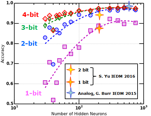
As seen in Fig. 1, even 2-bit weights achieve near-analog levels of accuracy with reasonably-sized, fully connected layers on a simple benchmark such as MNIST. Additionally, it is also possible to re-train a network to use larger layers if additional accuracy is required; choosing 2-bit weights therefore does not impose an overall inference accuracy constraint. Finally, it should be noted that the results of Fig. 1 are obtained by straightforward quantization of software-trained network (with the additional step of optimizing the quantization window). If the network is trained with the assumption of quantized weights, even better accuracy can be obtained.
II Architecture
The array architecture is a slightly modified resistive cross-bar array, as shown in Fig. 2. The standard approach of using two weights to represent positive and negative conductances is used. The modification of the standard approach arises only in the use of dedicated program lines; one for each bit and for each row of weights. The program lines are shared across the entire row of weights; selecting individual weights to program is accomplished using the select lines. In inference mode, the program lines are grounded, and the weights behave like two-terminal devices, forming a cross-bar between the signal input and output lines.
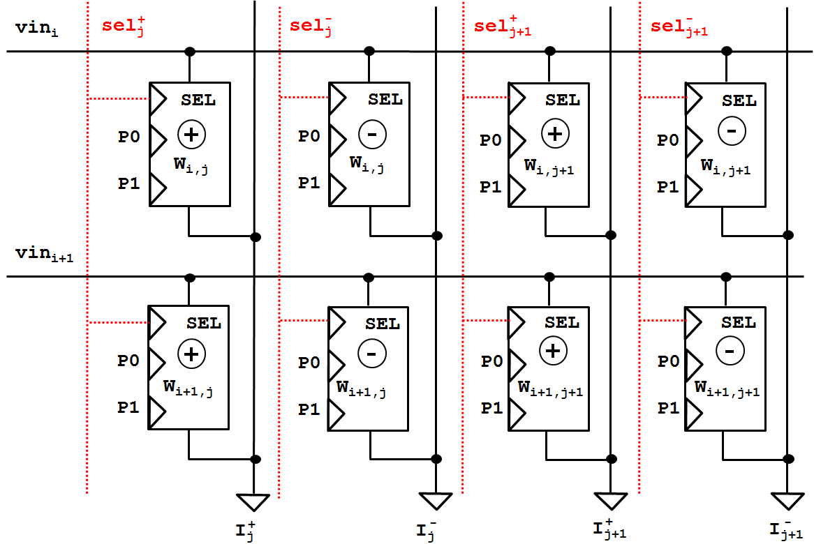
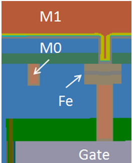
The resistive weight cells are composed of a parallel combination of passive resistors, with each passive resistor in series with a gating transistor (as illustrated in Fig. 3). The gating transistor could be a FeFET or a Flash transistor, or other FET-based NVM. In this work, we describe an architecture using a FeFET as the gating transistor, with the FeFET composed of a standard FET with a ferroelectric capacitor (FeCap) in the BEOL layers. The FeFET gate and BEOL physical structure is shown in Fig. 4. Electrically, this is similar to the integrated FeFET structure of [13].
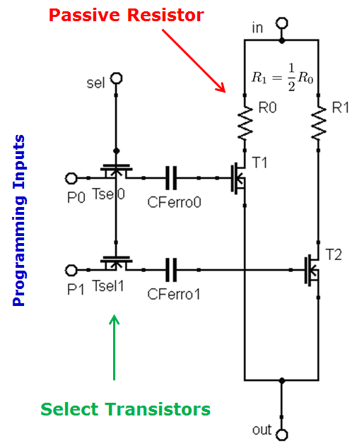
The resistance values of the passive resistors for the weight cell are chosen as etc. Conversely, the conductance of each branch (neglecting the influence of the transistors) is given by etc. Denoting the logic state of each transistor (indexed by ) as , the overall conductance of the cell is given as:
| (1) |
where is the number of bits in the cell ( in the example of Fig. 3). The state of the transistors is set by program and erase cycles (described in section IV), with the SEL input active. During inference, the program inputs () are grounded, and the potential on the gate of the transistors is determined by the polarization state of the ferroelectric capacitors. The programming is assumed to result in strongly-ON or strongly-OFF transistors (i.e. strongly negative or strongly positive Vt, respectively), resulting in branch conductances that are (ideally) independent of the properties of the transistors or the precise programming of the FeCaps.
III Ferroelectric Capacitor: Properties and Modeling
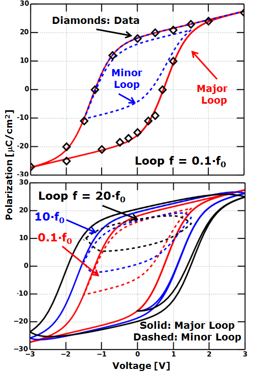
The FeCaps shown in Fig. 3 are the enablers for the non-volatile operation of the weight cell. The desirable property of the FeCaps is the hysteretic behavior of the polarization, as illustrated in Fig. 5 (using measured data from [10]).
In this work, the hysteretic behavior of FeCaps is modeled using a Preisach-based [9], turning-point model with explicit internal polarization dynamics. The quasi-static ferroelectric polarization is described next. The ”raw” response function is given by:
| (2) |
where is the voltage representing the internal state of the FeCap (related to the applied voltage, as described next), and model parameters describing the coercive voltages and the voltage scales, respectively. Likewise, is a model parameter which sets the polarization strength in each state. Each quantity in Eqn. 2 has a ”plus” and ”minus” label, depending on whether the capacitor last experienced an increase or decrease in applied voltage (respectively). This is referred to as the ”state” of the FeCap. The actual ferroelectric polarization is computed using Eqn. 3:
| (3) |
where the indices , denote the currently active turning points, with . Likewise, the quantities , , , and are evaluated at the current active pair of turning points. Eqn. 3 simply provides scaling and shifting of the raw response of Eqn. 2 to insure that the polarization curve passes through the active pair of turning points (this is necessary to provide reasonable minor-loop behavior). As is standard for turning-point models, turning points themselves are created and destroyed dynamically as the internal voltage of the FeCap switches. The ferroelectric response is thus modeled as a quasi-static function of the ”internal” state of the FeCap (described by ). The overall behavior of the FeCap is therefore dependent on the dynamics of . In this work, is governed by a second-order delay of the applied voltage across the FeCap. Specifically, the differential equation relating the ”internal” voltage and the applied voltage is given as:
| (4) |
where the natural frequency and the damping ratio are calibration parameters of the model. The ”memory” property of the FeCap is handled by the model though the turning point history and the active state. Both are changed in a discrete manner, when the temporal derivative of changes sign. This ensures that the state itself is not experiencing the second-order dynamics described in Eqn. 4; the dynamics merely provide a delay for an abrupt switching of the state. It should be noted that the second-order delay model of Eqn. 4 is purely empirical. It is merely used in this work to provide a delayed response for teh switching of ferroelectric domains. No attempt is made to provide a detailed frequency-dependence calibration to a specific material. It has been shown in the literature that the frequency response of ferroelectric materials covers a very wide range; from a very fast responses in the 10s of ns [11], to a much slower 10s of s [12]. For the purposes of this work, it is assumed that the ferroelectric material has a switching frequency comparable to the fast material of [11]. For materials where this is not the case, the programming times discussed in IV must be adjusted to accommodate the slower frequency response. Finally, the total charge of the capacitor is computed as:
| (5) |
where is the non-ferroelectric capacitance, and is the total capacitor area. The non-ferroelectric response is modeled as being driven by the instantaneous applied voltage , since the non-ferroelectric response is assumed to be much faster than any modulation of the applied voltage. For the purpose of this work, the complete model is implemented in Verilog-A and used within Synopsys HSPICE.
IV Program and Erase
In order to assign the weights of the neural network, the FeCaps must be programmed to appropriate states. This can be performed by applying voltage pulses to either the program terminals or the in/out terminals of the weight. Program and erase schemes for the FeCaps are illustrated in Fig. 6. In this work, a programming scheme which results in a positive after-pulse voltage on the gate node of the underlying FET is termed ”Program,” whereas a scheme which results in a negative after-pulse gate voltage is termed ”Erase.” In the example array of Fig. 2, a select transistor is needed in order to enable programming, since only a single set of program interconnect lines can be provided for each row of the crossbar array. Since the weights of a given row share program lines, the column which is being programmed at any given time is selected by activating the appropriate select line.
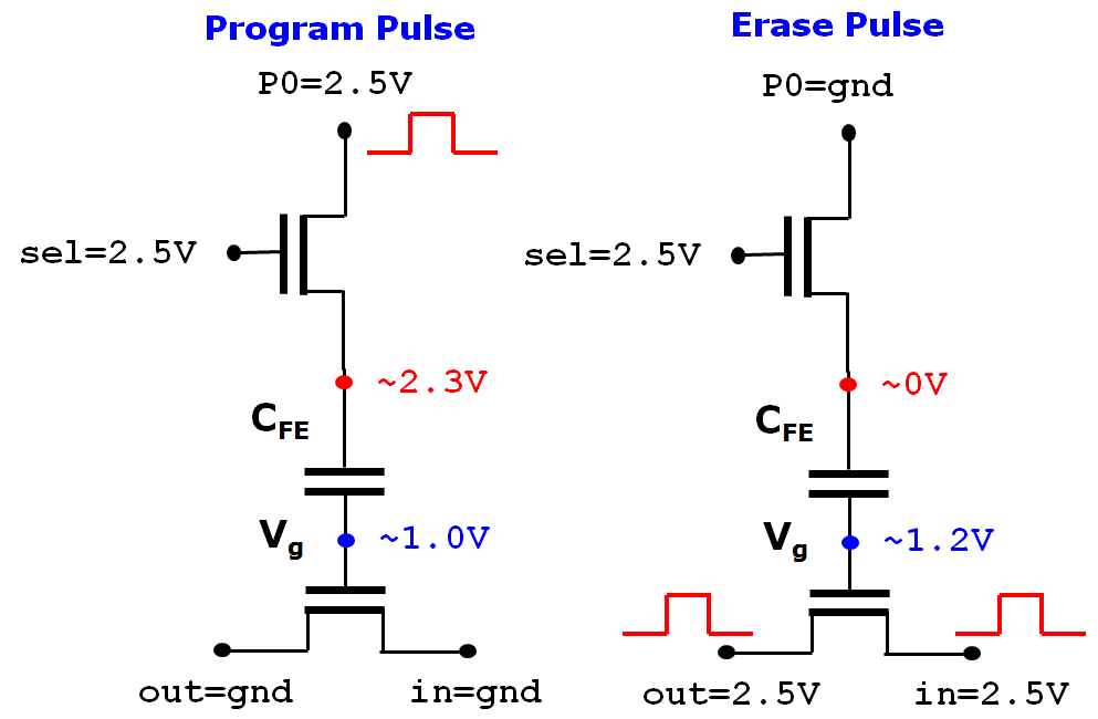
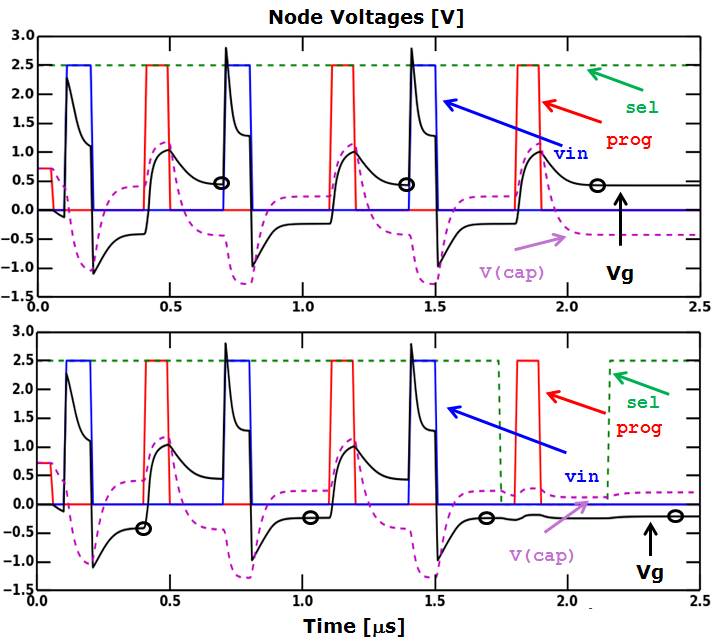
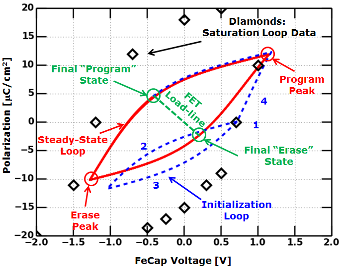
An additional constraint is the fact that the individual FeFETs of a given weight share common in/out terminals. It is therefore not possible to erase them individually, using the scheme of Fig. 6. One possible programming strategy is therefore to initially fully erase an array, with all FeCaps set to the erased state, followed by individual programming of FeCaps which need to be in the programmed states. This is somewhat akin to ”flash” erase commonly used for various Flash technologies. Both erase and program are expected to take place infrequently: only when the neural network is initially mapped onto the SoC. During inference operations (which are expected to be frequent), no erase or program operations take place. Figures 7 (top and bottom, respectively) illustrate program and erase events in more detail. In Fig. 7(top) a single bit is cycled several times by alternating erase and program pulses and ultimately left in a programmed state. The cycling is performed to ensure that the state of the bit is independent of the initial condition. The P-V trajectory for the erase-program cycle is illustrated in Fig. 8. Simulation begins with zero charge on the FeCap, in state 1. After the initial erase (arc 2), the first program pulse takes the FeCap to the highest achievable positive voltage, along arcs 3 and 4 of Fig. 8. This corresponds to the peak voltage point under the program pulse in Fig. 7. After the programming pulse ends (as is reduced to zero), the FeCap P-V trajectory continues along the steady-state loop (Fig. 8) until it intersects the FET load-line (the FET is now in strong inversion and has a nearly constant capacitance). The FET load line is simply established from the equation for the voltage drop across the FeFET stack:
| (6) |
After the program pulse is completed, Eqn. 6 reads simply , and with the condition that , the loadline can be established as
| (7) |
The equation for the loadline is approximate, since the FET gate capacitance is not constant. The final voltage across the FeCap after a programming even is negative (approximately -0.5V). Correspondingly, the voltage on the gate node of the FET is approximately positive 0.5V, putting the FET into a (relatively) weak ON-state. The is the ”Programmed” condition. The application of the erase pulse (achieved by simultaneously pulsing the in/out terminals while grounding the program terminal) makes the FeCap voltage more negative, continuing the P-V trajectory from the program point, all the way to the most negative voltage on the steady-state loop. After the erase pulse is completed, the P-V trajectory continues until it intersects the FET load-line at a slightly positive voltage. The slightly positive voltage of the FeCap with a grounded program line implies a slightly negative voltage on the gate of the FET (simulations indicate approximately -0.25V). Given that a typical Vt of the FET is approximately 350 mV, the erase cycle has left it in a strongly OFF condition. This is the ”Erased” condition.
While Fig. 7(top) left the FeCap in a programmed state, Fig. 7(bottom) illustrates how the erase (or rather, the ”non-program”) is accomplished instead. Since all FeCaps are initially erased, the select transistor is used to make sure that program events don’t change the state of FeCaps which must remain erased. The sel input is set to gnd during the last program pulse of 7, preventing programming from taking place. The final voltage on the gate of the FET is equal to that of the initial erased state. It should be noted from Fig. 8 that due to voltage division between the FeCap and the FET, the FeCaps in this example operate on a minor loop which is much smaller than the outer saturation loop. This indicates that much stronger programming is theoretically possible. In order to reach the saturation loop and correspondingly stronger ON-states of the FET, significantly higher programming voltages are required. Furthermore, the use of an nFET for the select device implies that the highest voltage across the FeFET is the lesser of and . High programming voltages therefore imply high values for the select device, suggesting that a high voltage design is required.
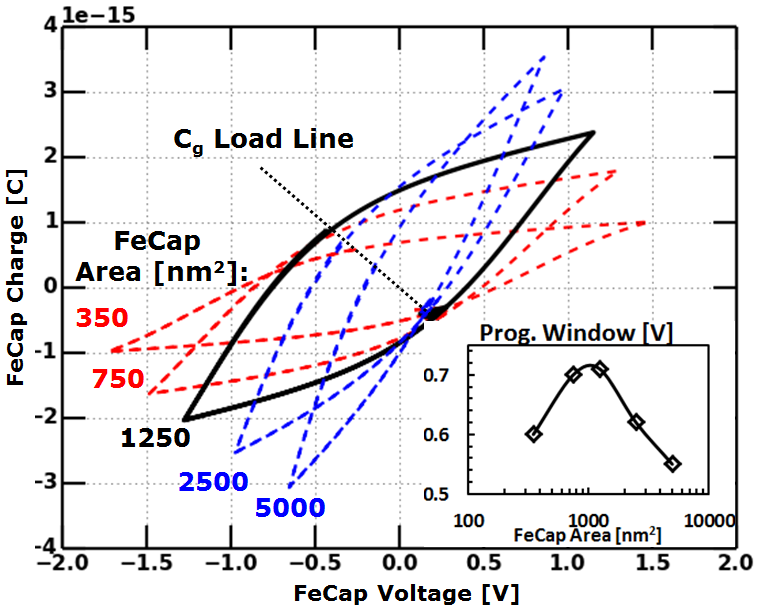
In this work, since the FeCaps are implemented in the BEOL levels, the area of the FeCaps is tunable and there is no layout area penalty associated with FeCap size. It is therefore possible to choose the FeCap area which maximizes the voltage window. The behavior of the program and erase loop as a function of FeCap area is illustrated in Fig. 9. Increasing the FeCap area results in a smaller voltage drop across the FeCap during programming. This constricts the size of the minor loop for the program/erase cycle, with lower end voltages and lower polarizations. This is seen in Fig. 9 as a tightening of the polarization loop with increasing area. At the same time, the increased area increases the total charge, resulting in higher peak charge values on the FeCap and FET gate (in spite of the reduced charge/unit area). This is reflected in Fig. 9 as higher peak charge values at the ends of the polarization loops. The final program and erase voltages are obtained from the intersection of each polarization loop with the zero- load line of the FET.
It can be seen that the locus of the intersection varies non-monotonically with FeCap area (especially for the program portion of the loop), due to the competing effects of reducing polarization and increasing area. The maximum in the voltage window is obtained for an FeCap area of 1250 nm2 (given the particulars of the underlying FETs and the FeCap hysteresis curve). Significantly larger or smaller areas result in degraded programming performance.
V Passive Resistor
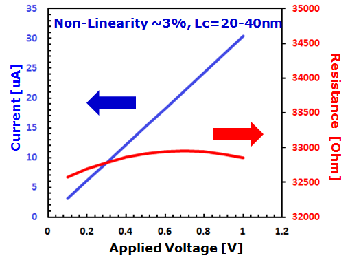
An important element of the multi-bit weight cell of Fig. 3 is the passive resistor. The resistance value of the resistor could be chosen so that when the FeFET in a branch of the cell is in the ON-state, the resistance of the passive resistor is much larger than that of the FET. If this is the case, then the non-linear behavior of the FET will have a negligible effect on the overall conductance of the cell. Given that the resistance of the FET is expected to be in the range of a few , the passive resistor should have a resistance in the range of to . Larger values of resistance result in better overall linearity, but also limit the current. With the stated resistance range, currents supplying the summing amplifiers are in the reasonable range of a few to a few tens of . There are many options for implementing the passive resistor, with varying tradeoffs on size, variability and linearity. One possible approach is to simply use the channel of a FET as the body of the passive resistor.
Simulations of such resistors (Fig. 10) indicate that the desired resistance level can be achieved with reasonably good linearity.
A concern with doped resistors is the RDF-induced variability. Unlike a FET with a doped channel, the question is not one of Vt-variability, but simply that of variable ”bulk” conductance due to the random number of dopants in any one resistor. As such, the variability of conductance (assuming Poisson-distributed number of dopants per channel) can be expressed as:
| (8) |
where is the conductance of the resistor body, is the RDF-induced standard deviation of the conductance, and is the total (expected) number of atoms in the resistor body. Given reasonable resistor dimensions, lengths, and target doping values, the expected number of atoms is ~100, resulting in a relative standard deviation of ~10%. While this may seem like a large uncertainty in the conductance (and therefore in the neural net weight), it is of relatively little consequence in typical fully-connected layers. This is illustrated in Fig. 11, where the accuracy of a neural net is evaluated with various levels of uncorrelated noise.
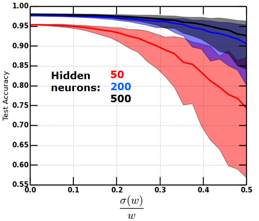
A single hidden-layer network with various sizes of the hidden layer is trained for MNIST. The weights are quantized to two-bit precision and perturbed using a Poisson distribution, as indicated by Eqn. 8. A set of MC simulations is then performed with various levels of perturbation. As can be seen from Fig. 11, there is no significant loss of classification accuracy until the relative weight perturbation is on the order of 30%. This is not surprising for for fully-connected architectures, such as the one used. The large number of inputs to any one neuron induce partial noise cancellation, with the expected standard deviation of the total input to the neuron scaling by , being the number of inputs. The larger the network layers then, the less susceptibility to uncorrelated weight noise there is. Given the expected level of 10%, the RDF of the resistors appears to be satisfactory.
VI Transistor
An important parameter of the underlying FET of the FeFET structure is the threshold voltage. There are typically two or three Vt levels provided, but the FeFET requirements place restrictions on the choice. This is illustrated in Fig. 12.
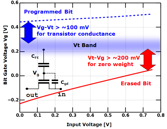
As seen in Fig. 12, the application of the input voltage to the weight cell causes a slight shift in the Vg node voltage. This is a result of the capacitive coupling of the FET drain and gate, both due to the parasitic and intrinsic coupled charge. The effect is particularly pronounced on erased bits, since very little current flows in the erased branch, and essentially the entire input voltage is applied to the drain of the FET. The IR drop across the resistor lessens the impact in branches with programmed bits. Fig. 12 illustrates a possible band of Vt values for the FET. For all applied input voltages, the erased transistor has a gate voltage significantly below the FET Vt. This ensures that the erased transistor remains turned off (the extent to which it is turned off is a technology parameter that sets the max ON/OFF ratio of the weights). The Vt is also low enough so that the programmed transistor has sufficient gate overdrive to keep the transistor conductance much higher than that of the passive resistor. Thus, the choice of the Vt falls into a somewhat narrow band, and induces a tradeoff between weight accuracy and linearity on one hand (Vt must be low), and low conductance of the zero weights (Vt must be high). Vt values in the 200-300 mV range needed for the implementation shown in this paper are typically readily available in modern CMOS technologies.
VII Results
Having programmed the individual FeFETs in the array, inference can be performed simply by applying input voltages (fixed levels or pulses) to the array. The program lines are all grounded during inference. In this mode, each weigh cell acts as a two-terminal device. For the case of the two-bit cell, the I-V characteristics are illustrated in Fig. 13.
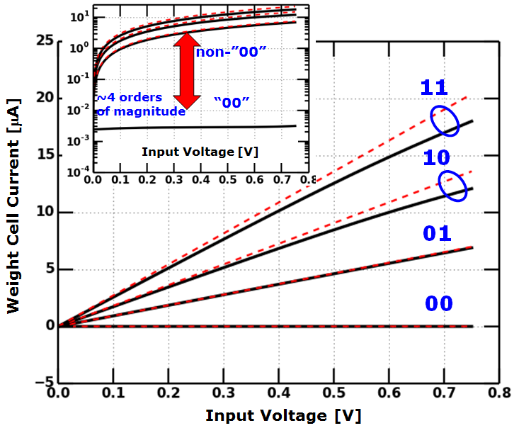
The I-V characteristics of Fig. 13 show good linearity over a wide range of input voltages, with appreciable deviation seen only for the highest current conditions. The dynamic range of ON/OFF currents is roughly four orders of magnitude, considerably larger than for memristive devices. This makes the multi-bit weight cell suitable for arrays with large numbers of inputs. The accuracy of the various ON-states is further illustrated in Fig. 14.
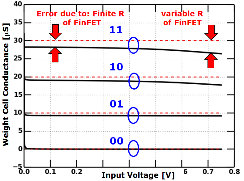
It is evident from Fig. 14 that the absolute accuracy of the weights is quite good when the weights are small, but the weights become increasingly less accurate as the nominal weight value increases. This is simply a result of the finite (and non-linear) resistance of the FET increasing the total series resistance. The effect is negligible for the small weights since the resistance of the passive resistor in those cases is large. Similarly, the accuracy is best for small values of the input signal but shows increasing error with the signal voltage. This is due to the transition of the FET from the linear to the saturation regime as the across the FET increases (particularly sensitive for large weight branches where the resistance of the passive resistor is small). Given the expected deviations of the hardware weights from ideality, it is necessary to simulate the accuracy of the overall neural net. The standard simple MNIST benchmark is used, as shown in Fig. 15. In addition to the quantized weights as described in this work, the neuronal activations are considered to be binarized. While this is certainly not necessary, binarization greatly simplifies the problem of transferring signals from one layer to the next, eliminating the need for ADC/DAC conversion.
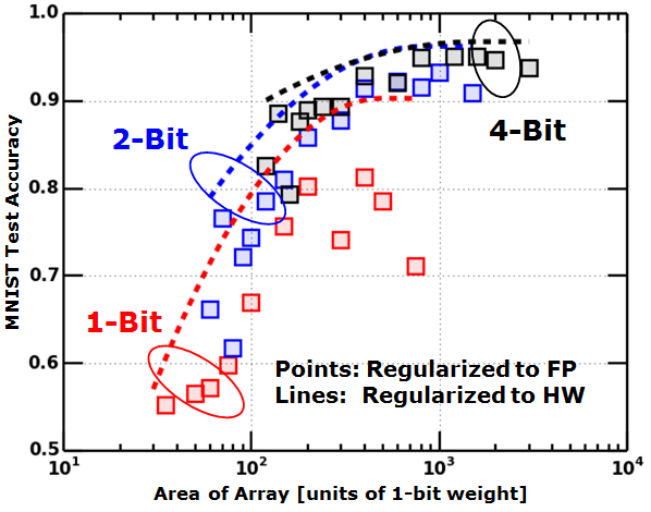
As can be seen in Fig. 15, the networks with non-ideal weights and binarized activations do indeed suffer some accuracy loss, as compared to ideal multi-bit weights (Fig. 1). The degree of accuracy loss depends on the regularization procedure, however. Points in Fig. 15 are obtained by direct quantization of weights from software-based training. Dashed lines are obtained using weights which were trained using hardware-aware regularization. While both sets of data use regularization, the inference on the validation set for the second group was performed using the full hardware model, including weight quantization, weight non-idealities, and binarization of activations. The algorithm is summarized in Alg. 1. The validation accuracy thus obtained is a much better estimate of the final test accuracy (which also uses non-ideal weights and activations), yielding much better test accuracies overall. This is particularly evident in cases where the neural network is over-provisioned (large arrays), and significant over-fitting occurs if the network is not properly regularized. With hardware-aware regularization, it can be seen that the test accuracy does not degrade for large arrays, and test accuracies are significantly better overall. Even better results should be obtainable if the training procedure itself is hardware-aware [14].
VIII Summary and Conclusion
A multi-bit weight cell for analog MAC in neuromorphic arrays was presented. The cell supports in-memory computing based on NVM-storage of weights, removing the need for DRAM access during inference (unlike GPU-like implementations such as [1]). It was shown that for inference purposes, a small number of bits are sufficient for analog-like accuracy. The proposed multi-bit weight cell uses an FeFET as gating element in each branch of a circuit consisting of a parallel combination branches of passive resistors. The resistor weights are arranged in a binary ladder, enabling a uniform distribution of conductances to be programmed into the cell. The FeFETs are constructed using standard FETs as the underlying FET element, with FeCaps in the BEOL connected to FET gates. The polarization state of the FeCaps stores the individual bits of the weight. It was suggested that passive resistors can be formed using FETs. The program and erase cycles for the cell were described, and it was found that moderately high voltages are needed for acceptable programming levels. It was found that up to 700 mV of differential programming (difference in FET Vt between programmed and erased states) could be achieved using standard CMOS processes and literature-based FeCap properties. With this level of programming, an acceptable level of weight linearity could be achieved, along with an ON/OFF ratio for the weights in excess of four orders of magnitude. Finally, it was shown that even with the non-ideal weights formed by the multi-bit circuits, a high level of inference accuracy is possible (using the MNIST benchmark). This is particularly true if the regularization is hardware-aware, i.e. cross-validation is performed using the actual weight model, with an optimized quantization window. . Failure to do so results in somewhat sub-optimal weight transfer from software to hardware, and an associated degradation in test accuracy. It was also noted that the area efficiency of the cell is independent of the number of bits used (except for the 1-bit case); at matched array area, the 2-bit and 4-bit cells produced the same level of inference accuracy. An unrecoverable loss was only observed with 1-bit cells. Further improvements in weight ideality require improved FeCap properties. Increased ferroelectric polarization (relative to the non-ferroelectric polarization) would result in increased Vt differentials between the programmed and erased states, enabling better linearity and further improved ON/OFF ratio.
References
- [1] N.P. Jouppi, et al., ”In-Datacenter Performance Analysis of a Tensor Processing Unit”, arXiv:1704.04760
- [2] Z. Li, P.Y. Chen, H. Xu, S. Yu, ”Design of Ternary Neural Network With 3-D Vertical RRAM Array IEEE Transactions on Electron Devices 64 (6), 2721-2727
- [3] P. Yao, H. Wu, B. Gao, N. Deng, S. Yu, H. Qian, ”Online training on RRAM based neuromorphic network: Experimental demonstration and operation scheme optimization”, Jun 13 2017 2017 IEEE Electron Devices Technology and Manufacturing Conference, EDTM 2017 - Proceedings. Institute of Electrical and Electronics Engineers Inc., p. 182-183 2 p. 7947592
- [4] S.B. Eryilmaz, D. Kuzum, S. Yu, H.S.P. Wong, ”Device and system level design considerations for analog-non-volatile-memory based neuromorphic architectures”, Feb 16 2016 Technical Digest - International Electron Devices Meeting, IEDM. Institute of Electrical and Electronics Engineers Inc., Vol. 2016-February, p. 4.1.1-4.1.4 7409622
- [5] S. Kim, M. Ishii, S. Lewis, T. Perri, M. BrightSky, W. Kim, R. Jordan, G.W. Burr, N. Sosa, A. Ray, J-P Han, C. Miller, K. Hosokawa, C. Lam, ”NVM neuromorphic core with 64k-cell (256-by-256) phase change memory synaptic array with on-chip neuron circuits for continuous in-situ learning” IEEE International Electron Devices Meeting (IEDM) 2015
- [6] G.W. Burr, R.M. Shelby, A. Sebastian, S. Kim, S. Kim, S. Sidler, K. Virwani, M. Ishii, P. Narayanan, A. Fumarola, L.L. Sanches, I. Boybat, M.L. Gallo, K. Moon, J. Woo, H. Hwang, Y. Leblebicim, ”Neuromorphic computing using non-volatile memory” Pages 89-124 — Received 31 Aug 2016, Accepted 01 Nov 2016, Published online: 04 Dec 2016
- [7] F.M. Bayat, X. Guo, M. Klachko, N. Do, K. Likharev, D. Strukov, ”Model-based high-precision tuning of NOR flash memory cells for analog computing applications”’, Proceedings of DRC’16, Newark, DE, June 2016
- [8] S. George, K. Ma, A. Aziz, X. Li, A. Khan, S. Salahuddin, M.F. Chang, S. Datta, J. Sampson, S. Gupta, V. Narayanan, ”Nonvolatile Memory Design Based on Ferroelectric FETs”, IEEE International Electron Devices Meeting (IEDM), 2016
- [9] G. Robert, D. Damjanovic, N. Setter ”Preisach modeling of ferroelectric pinched loops” Appl. Phys. Lett. 77, 4413 (2000)
- [10] J. Muller, , T.S. Boscke, D. Brauhaus, U. Schroder, U. Bottger, J. Sundqvist, P. Kücher, T. Mikolajick, L. Frey ”Ferroelectric Zr0.5Hf0.5O2 thin films for nonvolatile memory applications”, Appl. Phys. Lett. 99, 112901 (2011)
- [11] J. Li, B. Nagaraj, H. Liang, W. Cao, C. H. Lee, R. Ramesh, ”Ultrafast polarization switching in thin-film ferroelectrics” Appl. Phys. Lett. 84, 1174 (2004)
- [12] ”Experimental Study on Polarization-Limited Operation Speed of Negative Capacitance FET with Ferroelectric HfO2”, M. Kobayashi, N. Ueyama, K. Jang, T. Hiramoto, IEEE International Electron Devices Meeting (IEDM), 2016
- [13] S. George, K. Ma, A. Aziz, X. Li, A. Khan, S. Salahuddin, M.F. Chang, S. Datta, J. Sampson, S. Gupta, V. Narayanan, ”Nonvolatile Memory Design Based on Ferroelectric FETs”, IEEE International Electron Devices Meeting (IEDM), 2016
- [14] M. Rastegari, V. Ordonez, J. Redmon, A. Farhadi ”XNOR-Net: ImageNet Classification Using Binary Convolutional Neural Networks” , arXiv:1603.05279