Vector Electric Field Measurement via Position-Modulated Kelvin Probe Force Microscopy
Abstract
High-quality spatially-resolved measurements of electric fields are critical to understanding charge injection, charge transport, and charge trapping in semiconducting materials. Here, we report a variation of frequency-modulated Kelvin probe force microscopy (FM-KPFM) that enables spatially-resolved measurements of the electric field. We measure electric field components along multiple directions simultaneously by employing position modulation and lock-in detection in addition to numeric differentiation of the surface potential. We demonstrate the technique by recording linescans of the in-plane electric field vector in the vicinity of a patch of trapped charge in a DPh-BTBT organic field-effect transistor. This technique is simple to implement and should be especially useful for studying electric fields in spatially inhomogeneous samples like organic transistors and photovoltaic blends.
In this letter we describe a simple modification of frequency-modulated Kelvin probe force microscopyKikukawa, Hosaka, and Imura (1995) (FM-KPFM) that enables the direct spatial imaging of electric field components near a surface along multiple directions simultaneously. The lateral electric field in an FM-KPFM measurement has to date been acquired by numerically differentiating the measured surface potential versus position data to obtain the electric field versus position Burgi, Sirringhaus, and Friend (2002); Silveira and Marohn (2004); Ng, Silveira, and Marohn (2007); Slinker et al. (2007); Pingree et al. (2007). Here we show how to microscopically measure multiple electric field components simultaneously using sample-position modulation and lock-in detection. In measurements of the electric field perpendicular to the fast-scan direction, our position-modulation technique improved spatial resolution by a factor of four compared to numerical differentiation of the FM-KPFM surface potential image.
Microscopically measuring electric fields can be helpful for understanding both device physics and materials properties. Bürgi et al. showed experimentally that the potential measured by FM-KPFM above a transistor reflected the electrostatic potential of the accumulation layer at the transistor’s buried semiconductor-insulator interface Burgi, Sirringhaus, and Friend (2002). This finding was subsequently justified theoretically by Silveira, Dunlap, and coworkers Silveira et al. (2007). Building on this observation, Bürgi and coworkers introduced the idea of using the locally-inferred electric field, the locally-inferred electrostatic potential, and the measured bulk current to infer the mobility at each location in the channel of a polymer field-effect transistor Burgi, Sirringhaus, and Friend (2002). The thus-measured mobility was analyzed as a function of temperature and local electric field to draw conclusions concerning charge-transport mechanisms in the polymeric semiconducting material. If an abrupt voltage drop is apparent at a transistor contact, then the contact resistance can be computed by dividing the observed voltage drop by the measured current and likewise studied versus temperature and injecting-contact composition Burgi et al. (2003). In samples where no such voltage drop is apparent, Silveira et al. showed that charge injection could nevertheless be studied microscopically by simultaneously measuring the device current and the lateral electric field at the injecting contact as a function of applied voltage and temperature; plots of the current versus the electric field could be directly compared to charge-injection theory Silveira and Marohn (2004); Ng, Silveira, and Marohn (2007). This procedure was used to assign an “ohmicity” to the metal-organic contact in a two-terminal device exhibiting no potential drop at the injecting contactNg, Silveira, and Marohn (2006). Recent work has extended FM-KPFM’s ability to map the distribution of trapped or mobile charges Ando et al. (2014); Murawski et al. (2015a, b); Yamagishi et al. (2016) as a function of time or frequency. Experimental protocols have also been developed to allow FM-KPFM to make quantitative measurements of surface potential even in the presence of parasitic capacitances Ito et al. (2011); Fuller et al. (2013). The method introduced here was designed to expand KPFM’s ability to make electric field measurements with high spatial resolution.

Below we report measurements over an organic field-effect transistor made from the hole-transporting small molecule DPh-BTBT Takimiya et al. (2006). We used DPh-BTBT because it is an air-stable small molecule that can be easily evaporated to produce high-mobility field-effect transistors (). To fabricate the transistor, we evaporated nanometers of DPh-BTBT onto a room-temperature transistor substrate at a rate of . The transistor substrates were cleaned before use by sonicating in 1:1 acetone:isopropyl alcohol for 15 min, scrubbing and sonicating 10 min with distilled water and detergent (Aquet), sonicating in distilled water 10 min, and ozone cleaning for 5 min. The transistor substrate was comprised of a highly -doped silicon gate, a thermally grown silicon oxide insulator layer, and -thick gold source and drain electrodes with a chromium adhesion layer. The electrodes were deposited using thermal evaporation and patterned into an interdigitated array. The channel length was and the total channel width was .
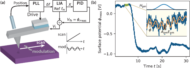
In FM-KPFM (Fig. 1a), the sample’s surface potential is determined by oscillating the cantilever at its resonance frequency using a phase-locked loop controller and nulling the cantilever frequency shift induced by tip-sample electrostatic forces
| (1) |
with the cantilever resonance frequency, the cantilever spring constant, the second derivative of the tip-sample capacitance with respect to the vertical direction, the cantilever tip voltage, and the sample’s surface potential. The applied tip voltage is the sum of a fixed-frequency modulation voltage and a feedback voltage : , where is the voltage-modulation amplitude and is the voltage-modulation frequency. A lock-in amplifier measures the oscillating frequency shift at the modulation frequency
| (2) |
A proportional-integral-derivative controller feedback loop adjusts to maintain at zero. With large enough feedback gain, , and the feedback voltage tracks the surface potential closely: . The feedback voltage is the measured surface potential. The assumption that is only valid at low frequencies or long times. The feedback voltage also varies due to the effects of detector noise, low-frequency position noise, and surface potential fluctuations.
Many KPFM measurements derive information mainly from contrast in surface potential images or the average difference in surface potential over different regions of the sample. These properties are relatively insensitive to feedback loop dynamics, noise, and surface potential fluctuations. In contrast, these sources of error affect the calculated electric field dramatically. To highlight the effect of these error sources, we write the measured surface potential as
| (3) |
where is the feedback loop’s impulse response function, denotes convolution in the time domain, is the sample’s actual surface potential and is an equivalent surface potential noise that accounts for noise in .
Noise in the measured surface potential typically arises from two sources: cantilever position noise and low-frequency surface potential noise. The effect of cantilever position noise can be minimized by operating at a sufficiently large modulation voltage or cantilever amplitude. Low-frequency surface potential noise could arise from position hysteresis and noise or real surface potential fluctuations caused by trapped charge or dielectric fluctuations Hoepker et al. (2011); Lekkala et al. (2012); Lekkala, Marohn, and Loring (2013). In either case, the effect of surface potential noise can be mitigated by increasing the scan speed.
Increasing the scan speed, however, comes at a cost. The feedback loop response function has a bandwidth . This temporal bandwidth limits the spatial resolution of the measured surface potential and electric field when the tip is scanned Garrett and Munday (2016). For a tip velocity , the measurement response function distorts the surface potential and electric field when they change on a length scale smaller than . We find significant distortion near the contact of a DPh-BTBT transistor when (Fig. S2).
If the scan speed is carefully optimized, low-frequency surface potential noise along the scan axis can be avoided without distorting the measured electric field significantly. In a 2D raster scan, however, the electric field measured along the slow scan axis will still be subject to large low-frequency () surface potential noise caused by position hysteresis and slow surface potential fluctuations.
To avoid this low-frequency noise, we modify the KPFM measurement by adding a small position modulation . The position modulation allows us to measure the electric-field component along the position-modulation direction , since to first order in
| (4) |
We use a modulation having a direction or and a magnitude
| (5) |
with the modulation amplitude and the modulation frequency. We detect the electric field as an oscillating potential at the modulation frequency with amplitude . To measure accurately, the modulation amplitude must be small enough that the potential can be approximated to first order in as in Eq. 4. The position-modulation technique could be combined with any KPFM technique that may be used to measure the sample’s surface potential, including amplitude-modulation KPFM Nonnenmacher, O’Boyle, and Wickramasinghe (1991), heterodyne KPFM Sugawara et al. (2012); Garrett and Munday (2016), dissipative KPFM Miyahara et al. (2015); Miyahara and Grutter (2017), or open-loop KPFM Takeuchi et al. (2007); Collins et al. (2013). We demonstrate the position-modulation technique in combination with FM-KPFM in this paper and call the combined protocol pm-FM-KPFM. Because we detect using the FM-KPFM feedback loop, the modulation frequency must be significantly smaller than the feedback loop bandwidth . In our measurements, we used and , with over the gate and over the source/drain electrodes (noting that ).
To perform the pm-FM-KPFM measurement, we used the experimental setup from Figure 1a and saved the measured surface potential -versus-time data (digitized at ). The surface potential-versus-time data measures the surface potential and electric field in the scan direction at low frequencies and the electric field in the modulation direction at the modulation frequency. We low-pass filtered using the filter to estimate the sample surface potential along the scan direction. We processed again using a software lock-in amplifier with lock-in filter to extract the electric field along the modulation direction
| (6) |
where is the in-phase component of the software lock-in amplifier (supporting material S3). In writing Eq. 6, we neglect a correction term that depends on the spatial dependence of the tip-sample capacitance , the sample topography, and the position-modulation amplitude . For our sample and experimental conditions, the correction term would cause a worst-case fractional error in the electric field of less than 0.1 percent (supporting material S4). If this correction term were problematically large, changes in could be corrected for by using the component of the cantilever frequency shift at , as in open-loop KPFM measurements Takeuchi et al. (2007); Collins et al. (2013). The Fig. 1b inset shows this analysis in a representative region near the contact where along the scan direction is relatively constant and the electric field along the modulation direction is significant.

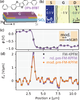
To verify the accuracy of the electric field calculated using pm-FM-KPFM, we performed pm-FM-KPFM and FM-KPFM line scans across a DPh-BTBT thin-film transistor (Fig. 2). So that both techniques measure , we applied the position modulation along the scan axis (Fig. 2c inset). The data in Fig. 2c confirms that the two techniques measure the same surface potential . We low-pass filtered the surface potential at , which corresponds to a spatial frequency low-pass filter at .
From the two line scans, we calculated the electric field three ways (Fig. 2d). We numerically differentiated the FM-KPFM surface potential (squares) and the pm-FM-KPFM surface potential (triangles). To calculate the electric field from the position-modulation signal, we processed the raw surface potential data using a software lock-in amplifier whose reference frequency was set equal to the position-modulation frequency . To make a fair comparison to standard FM-KPFM, we used a bandwidth lock-in amplifier filter, identical to the filter used for the surface potential. We plot the electric field , where is the in-phase channel of the phased lock-in amplifier output (circles). The electric field and surface potential calculated from pm-FM-KPFM agree with the FM-KPFM electric field and surface potential. At equivalent bandwidth, all three electric field measurements have similar noise.


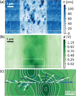
Above we argued that pm-FM-KPFM should be useful to measure the electric field along the slow scan axis with greater signal-to-noise. As a demonstration, we collected AFM and FM-KPFM images over the DPh-BTBT transistor with source, gate, and drain voltages set to zero (Fig. 3(a,b)). The FM-KPFM image revealed pockets of trapped charge in the transistor channel (dark spots in box in Fig. 3b).
To probe the electric field near these trapped charges, we took a pm-FM-KPFM linescan (Fig. 3c; Fig. 4). We applied the position modulation perpendicular to the scan direction so that we measured and simultaneously; was determined by numerically differentiating the measured with respect to the fast scan direction while was obtained from as discussed above. Figure 3c shows the KPFM image contours along with the in-plane electric field vector measured by pm-FM-KPFM. One consequence of the electric field being the negative gradient of the electrostatic potential is that the electric field vector at location must be perpendicular to a line tangent to the constant- surface passing through . This perpendicular relationship is clearly evident in Fig. 3c, demonstrating pm-FM-KPFM’s ability to serve as a vector electrometer.
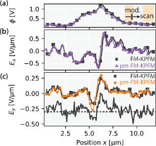
In Figure 4, we quantitatively compare the surface potential and the electric field measured by FM-KPFM and pm-FM-KPFM. Both measurements computed the electric field along the fast scan axis () by numerical differentiation, using surface potential data averaged for in each case. The two measurements of are in close agreement (Fig. 4b). We evaluate spatial resolution using the spatial frequency 3-dB bandwidth, defined as the frequency at which the measured electric field captures percent of the actual electric field signal. The measurements of both have a bandwidth of .
Figure 4c shows the electric field along the slow scan axis . We plot the pm-FM-KPFM (light circles) along with two calculations of obtained from the FM-KPFM image of the sample’s surface potential. The dark squares show a filtered FM-KPFM , with the 3-dB spatial bandwidth along the -axis limited to using a 17-point low-pass filter. The pm-FM-KPFM spatial bandwidth is , limited by the magnitude of the position-modulation amplitude . Even with a bandwidth along the -axis nearly 4-times greater, the pm-FM-KPFM electric field has similar or lower noise than the FM-KPFM electric field.
For comparison, in Fig. 4c we also we plot the unfiltered FM-KPFM (offset by ). The unfiltered has a spatial bandwidth , limited by the spacing between data points . Despite having a factor of two lower bandwidth than the pm-FM-KPFM measurement, the FM-KPFM signal exhibits significantly worse noise. We can understand this observation by noting that the FM-KPFM was computed by subtracting surface potential points acquired apart. Slow drift in the surface potential on this timescale thus shows up as noise in the FM-KPFM-inferred Schumacher et al. (2016). Viewing the measurements in the frequency domain, the FM-KPFM measurement of incorporates surface potential noise at temporal frequencies near . The pm-FM-KPFM measurement of incorporates surface potential noise at frequencies near , where overall surface potential noise is near a minimum (Fig. S6). This advantage in signal-to-noise ratio can be used to achieve higher spatial resolution at equivalent bandwidth or lower noise at equivalent spatial resolution. Moreover, pm-FM-KPFM allows to be measured simultaneously with .
We anticipate that the simple modification of KPFM introduced here will facilitate electric field measurements in a variety of systems. It is increasingly recognized that transistor measurements significantly overestimate charge mobility in high-performance organic semiconductorsMcCulloch, Salleo, and Chabinyc (2016); Bittle et al. (2016); 1D electric field mapping, in conjunction with current measurements, offers a general route to avoiding this materials-characterization pitfall. Although we demonstrate its use for measuring lateral electric fields, it should also be possible to measure vertical electric fields with an additional vertical position modulation. The local electric field vectors measured here are already an advance from lateral electric field line scans, and we envision applying the pm-FM-KPFM technique to measure local electric fields in bulk heterojunction solar cell blends Luria et al. (2012); Tennyson et al. (2015) and other composite materials Cadena et al. (2016). KPFM measurements mimic device operation near the open-circuit voltage condition; acquiring 2D electric field scans would allow the visualization of the current flow direction at domain boundaries in illuminated films near the condition.
The supplementary materials contain details of the experimental setup, data analysis, and experimental noise. The experimental data are available online Dwyer et al. (2017). The authors acknowledge support from Cornell University and the National Science Foundation through an NSF Graduate Research Fellowship (L.M.S.), NSF-DMR 1309540, and NSF-DMR 1602951. This work was performed in part at the Cornell NanoScale Facility, a member of the National Nanotechnology Coordinated Infrastructure (NNCI), which is supported by the National Science Foundation (Grant ECCS-1542081).
References
- Kikukawa, Hosaka, and Imura (1995) A. Kikukawa, S. Hosaka, and R. Imura, Appl. Phys. Lett. 66, 3510 (1995).
- Burgi, Sirringhaus, and Friend (2002) L. Burgi, H. Sirringhaus, and R. Friend, Appl. Phys. Lett. 80, 2913 (2002).
- Silveira and Marohn (2004) W. R. Silveira and J. A. Marohn, Phys. Rev. Lett. 93, 116104 (2004).
- Ng, Silveira, and Marohn (2007) T. N. Ng, W. R. Silveira, and J. A. Marohn, Phys. Rev. Lett. 98, 066101 (2007).
- Slinker et al. (2007) J. D. Slinker, J. A. DeFranco, M. J. Jaquith, W. R. Silveira, Y.-W. Zhong, J. M. Moran-Mirabal, H. G. Craighead, H. D. Abruña, J. A. Marohn, and G. G. Malliaras, Nat. Mater. 6, 894 (2007).
- Pingree et al. (2007) L. S. C. Pingree, D. B. Rodovsky, D. C. Coffey, G. P. Bartholomew, and D. S. Ginger, J. Am. Chem. Soc. 129, 15903 (2007), pMID: 18052165.
- Silveira et al. (2007) W. R. Silveira, E. M. Muller, T. N. Ng, D. H. Dunlap, and J. A. Marohn, in Scanning Probe Microscopy: Electrical and Electromechanical Phenomena at the Nanoscale, Vol. II, edited by S. V. Kalinin and A. Gruverman (Springer Verlag, New York, 2007) pp. 788 – 830.
- Burgi et al. (2003) L. Burgi, T. Richards, R. Friend, and H. Sirringhaus, J. Appl. Phys. 94, 6129 (2003).
- Ng, Silveira, and Marohn (2006) T. N. Ng, W. R. Silveira, and J. A. Marohn, Proc. SPIE 6336, 63360A (2006).
- Ando et al. (2014) M. Ando, S. Heike, M. Kawasaki, and T. Hashizume, Appl. Phys. Lett. 105, 193303 (2014).
- Murawski et al. (2015a) J. Murawski, T. Graupner, P. Milde, R. Raupach, U. Zerweck-Trogisch, and L. M. Eng, J. Appl. Phys. 118, 154302 (2015a).
- Murawski et al. (2015b) J. Murawski, T. Mönch, P. Milde, M. P. Hein, S. Nicht, U. Zerweck-Trogisch, and L. M. Eng, J. Appl. Phys. 118, 244502 (2015b).
- Yamagishi et al. (2016) Y. Yamagishi, K. Kobayashi, K. Noda, and H. Yamada, Appl. Phys. Lett. 108, 093302 (2016).
- Ito et al. (2011) M. Ito, Y. Hosokawa, R. Nishi, Y. Miyato, K. Kobayashi, K. Matsushige, and H. Yamada, e-J. Surf. Sci. Nanotech. 9, 210 (2011).
- Fuller et al. (2013) E. J. Fuller, D. Pan, B. L. Corso, O. Tolga Gul, J. R. Gomez, and P. G. Collins, Appl. Phys. Lett. 102, 083503 (2013).
- Takimiya et al. (2006) K. Takimiya, H. Ebata, K. Sakamoto, T. Izawa, T. Otsubo, and Y. Kunugi, J. Am. Chem. Soc. 128, 12604 (2006).
- Hoepker et al. (2011) N. Hoepker, S. Lekkala, R. F. Loring, and J. A. Marohn, J. Phys. Chem. B 115, 14493 (2011).
- Lekkala et al. (2012) S. Lekkala, N. Hoepker, J. A. Marohn, and R. F. Loring, J. Chem. Phys. 137, 124701 (2012).
- Lekkala, Marohn, and Loring (2013) S. Lekkala, J. A. Marohn, and R. F. Loring, J. Chem. Phys. 139, 184702 (2013).
- Garrett and Munday (2016) J. L. Garrett and J. N. Munday, Nanotechnology 27, 245705 (2016).
- Nonnenmacher, O’Boyle, and Wickramasinghe (1991) M. Nonnenmacher, M. O’Boyle, and H. Wickramasinghe, Appl. Phys. Lett. 58, 2921 (1991).
- Sugawara et al. (2012) Y. Sugawara, L. Kou, Z. Ma, T. Kamijo, Y. Naitoh, and Y. Jun Li, Appl. Phys. Lett. 100, 223104 (2012).
- Miyahara et al. (2015) Y. Miyahara, J. Topple, Z. Schumacher, and P. Grutter, Phys. Rev. Appl. 4 (2015), 10.1103/PhysRevApplied.4.054011.
- Miyahara and Grutter (2017) Y. Miyahara and P. Grutter, Appl. Phys. Lett. 110, 163103 (2017).
- Takeuchi et al. (2007) O. Takeuchi, Y. Ohrai, S. Yoshida, and H. Shigekawa, Jpn. J. Appl. Phys. 46, 5626 (2007).
- Collins et al. (2013) L. Collins, J. I. Kilpatrick, S. a. L. Weber, A. Tselev, I. V. Vlassiouk, I. N. Ivanov, S. Jesse, S. V. Kalinin, and B. J. Rodriguez, Nanotechnology 24, 475702 (2013).
- Schumacher et al. (2016) Z. Schumacher, Y. Miyahara, A. Spielhofer, and P. Grutter, Phys. Rev. Applied 5, 044018 (2016).
- McCulloch, Salleo, and Chabinyc (2016) I. McCulloch, A. Salleo, and M. Chabinyc, Science 352, 1521 (2016).
- Bittle et al. (2016) E. G. Bittle, J. I. Basham, T. N. Jackson, O. D. Jurchescu, and D. J. Gundlach, Nat. Comms. 7, 10908 (2016).
- Luria et al. (2012) J. L. Luria, N. Hoepker, R. Bruce, A. R. Jacobs, C. Groves, and J. A. Marohn, ACS Nano 6, 9392 (2012).
- Tennyson et al. (2015) E. M. Tennyson, J. L. Garrett, J. A. Frantz, J. D. Myers, R. Y. Bekele, J. S. Sanghera, J. N. Munday, and M. S. Leite, Adv. Energy Mater. , 1501142 (2015).
- Cadena et al. (2016) M. J. Cadena, S. H. Sung, B. W. Boudouris, R. Reifenberger, and A. Raman, ACS Nano 10, 4062 (2016).
- Dwyer et al. (2017) R. P. Dwyer, L. M. Smieska, A. M. Tirmzi, and J. A. Marohn, “Data and analysis for “Vector electric field measurement via position-modulated Kelvin probe force microscopy”,” Available from http://github.com/ryanpdwyer/1704-pmkpfm (2017).