Atomic-layer doping of SiGe heterostructures for atomic-precision donor devices
Abstract
As a first step to porting scanning tunneling microscopy methods of atomic-precision fabrication to a strained-Si/SiGe platform, we demonstrate post-growth P atomic-layer doping of SiGe heterostructures. To preserve the substrate structure and elastic state, we use a T C process to prepare clean Si0.86Ge0.14 surfaces suitable for atomic-precision fabrication. P-saturated atomic-layer doping is incorporated and capped with epitaxial Si under a thermal budget compatible with atomic-precision fabrication. Hall measurements at T K show that the doped heterostructure has R , yielding an electron density cm-2 and mobility cm2 V-1 s-1, similar to saturated atomic-layer doping in pure Si and Ge. The magnitude of and the complete absence of Shubnikov-de Haas oscillations in magnetotransport measurements indicate that electrons are overwhelmingly localized in the donor layer, and not within a nearby buried Si well. This conclusion is supported by self-consistent Schrödinger-Poisson calculations that predict electron occupation primarily in the donor layer.
I Introduction
Atomic-precision fabrication via scanning tunneling microscopy (STM) hydrogen depassivation lithography has blossomed as a unique route to form doped-Si and Ge nanoelectronics with single-atom selectivity and feature sizes Ruess et al. (2004); Shen et al. (2004); Ruess et al. (2007); Fuechsle et al. (2012); Scappucci et al. (2009, 2011). Atomic-precision is enabling for Si quantum computing research Zwanenburg et al. (2013); Kane (1998); Vrijen et al. (2000); Fang et al. (2005); Hollenberg et al. (2006); Hill et al. (2015); Koiller et al. (2001); Gamble et al. (2015) with potential utility in other fields such as limit-testing in scaling and quantum confined geometries in conventional microelectronics Koenraad and Flatté (2011); Pok et al. (2007); Weber et al. (2014); Scrymgeour et al. (2017); Gramse et al. (2017).
A step to facilitate broader electronic device applications is to integrate atomic-precision doping into vertically-gated configurations incorporating metal-insulator-semiconductor (MIS) capacitors Scappucci et al. (2007); Fuechsle et al. (2007); Lee et al. (2010). For example, the archetypal Kane proposal utilizes single donors placed in MIS stacks Kane (1998); Vrijen et al. (2000); Fang et al. (2005); Hollenberg et al. (2006). To protect atomic-precision donors from disordering via diffusion, the thermal budget to integrate a gate stack is constrained to temperatures too low for ideal SiO2 growth by furnace oxidation Goh et al. (2008); Sullivan et al. (2004); Keizer et al. (2015). This has inspired attempts to integrate gate stacks using insulators grown by lower-temperature methods. Unfortunately, these yield more defective films and disorder with measurable effects on donor device performance Fuechsle et al. (2007); Lee et al. (2010).
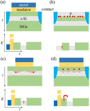
Strained-layer band-offset engineering via thin-film heteroepitaxy is a mature technique to form an interfacial barrier at a relatively low growth thermal budget Lee et al. (2005); Vrijen et al. (2000). Layered strained-Si (s-Si) and SiGe heterostructures have the benefit of pristine all-epitaxial interfaces with disorder that compares well with the highest-quality Si/SiO2 interfaces Lee et al. (2005); Friesen et al. (2003). As a measure of disorder, exceptional Si/SiO2 field-effect devices undergo a K metal insulator transition at critical electron densities - cm-2 with peak mobilities - cm2V-1s-1 Pudalov et al. (1993); Kim et al. (2017). By comparison, good SiGe field-effect devices turn on at - cm-2 achieving peak - cm2V-1s-1 Lai et al. (2005); Lu et al. (2009); Laroche et al. (2015); Mi et al. (2015); Zajac et al. (2015). In our SiGe substrate, we find cm-2 and peak cm2V-1s-1 at T K prior to adding atomic-layer doping Laroche et al. (2015). Fig. 1 (a) shows a schematic of the field-effect device used to characterize transport in the s-Si well (see Ref. Laroche et al., 2015). Fig. 1 (b) shows our device to test transport after atomic-layer doping.
Integrating atomic-precision doping with SiGe heterostructures leverages advantages of all-epitaxial order inherent in both platforms. A few works have proposed donor spin qubits in s-Si/SiGe Vrijen et al. (2000); Fang et al. (2005). Fig. 1 (c) shows a simplified sketch for a 2-qubit interaction. Qubit control would be via MIS gating to move electrons on and off the nucleus, or into SiGe layers, to tune spin precession. Spins would couple by drawing electrons to heterointerfaces, e.g., to form 2-electron quantum dots. Spin initialization and readout would be by established methods using single-electron transistors formed by MIS accumulation in the well Vrijen et al. (2000); Fang et al. (2005). Another potential application is 2D atomic-precision modulation doping to investigate effects of carefully tuned ordered potentials on 2D electron transport at heterostructure interfaces, which may permit tailor-made electronic band structures enforced by donor periodicity Koenraad and Flatté (2011). Fig 1 (d) shows a schematic of a field-effect device with ordered modulation doping in the channel. Ordered doping potentials promote channel mobility, with anticipated applications in high-electron mobility transistors Lee et al. (2005).
Here, we demonstrate atomic-layer doping of a s-Si/SiGe heterostructure via a thermal process entirely compatible with STM atomic-precision fabrication and our epitaxial SiGe heterostructure, which can withstand T 850∘C annealing Klauk et al. (1996). We incorporate P atomic-layer doping into the heterostructure by a process thermally compatible with atomic-precision fabrication. Results of each process step are characterized and contrasted with outcomes on relaxed bulk Si. Post-growth secondary ion mass spectroscopy (SIMS) yields an integrated P density, cm-2 with a full width at half maximum (FWHM)3 nm, similar to results demonstrated for pure Si and Ge Oberbeck et al. (2002); Scappucci et al. (2009). Hall effect measurements show that the doped heterostructure has an electron density, cm-2 and mobility cm2V-1s-1. These numbers are consistent with electron transport predominantly in the atomic-layer doping. Magnetotransport measurements to 8 T reveal only a small B0 T weak-localization bump, characteristic of transport via the atomic-layer doping, and no sign of Shubnikov-de Haas oscillations characteristic of transport via the high-mobility strained Si well Laroche et al. (2015). Self-consistent Schrödinger-Poisson calculations confirm the intuitive picture that electrons primarily populate the donor layer.
II Device fabrication and physical characterization
Atomic-precision fabrication has been demonstrated on (100)-oriented Si Ruess et al. (2004); Shen et al. (2004); Ruess et al. (2007); Fuechsle et al. (2012), Ge Scappucci et al. (2009, 2011), strained-Si on insulator (s-SOI) Lee et al. (2013, 2014), and Ge on insulator Klesse et al. (2013). Needless to say, the recipes differ between each, owing to unique thermal and chemical considerations, cf materials-specific growth recipes for molecular beam epitaxy (MBE) of Si vs Ge Ishizaka and Shiraki (1986); Okumura et al. (1998). In principle, s-SOI also provides a platform for strained-layer band engineering, but we consistently find that the s-SOI surface is rough on a nanometer-scale owing to bulk-elasticity-driven step-bunching Lee et al. (2013, 2014); Tersoff et al. (1995). Therefore, we have chosen to investigate donor placement on the relaxed SiGe surface, which as we will show, does not suffer from the inherent step bunching problem.
We perform atomic-layer doping in an ultrahigh vacuum (5 Torr) scanning tunneling microscope (UHV STM) equipped with a phosphine (PH3) gas source and a Si MBE source (joule heated solid Si, homebuilt). The substates for our experiments are s-Si/Si0.86 Ge0.14 heterostructures grown by UHV chemical vapor deposition using SiH4 and GeH4 as precursors at T550 ∘C. The substrates for our experiments have a 20-nm-thick s-Si well and a 50-nm-thick relaxed Si0.86Ge0.14 cap. Further details about the substrate growth and characterization can be found in Ref. Laroche et al., 2015.
Prior to atomic-layer doping experiments, we perform an ex-situ wet chemical cleaning procedure, and annealing in the UHV STM. The samples are cleaned by three cycles of chemical oxidation ( H2SOH2O2, 90 ∘C, 5 mins) and reduction ( NH4F:HF, 10 s), followed by a rinse in deionized H2O. Samples are exceptionally hydrophobic upon extraction (presumably hydrogen terminated). Two different chemical and annealing recipes yield suitably clean flat surfaces for atomic layer doping: (1) the H-terminated samples can be loaded into the UHV system and annealed at a temperature sufficient to desorb the hydrogen (650 ∘C, 15 s), or (2) samples can be oxidized (5:1:1 H2O:H2O2:HCl, 60 ∘C, 5 mins), then annealed hotter (T800 ∘C, 20 mins) to remove the chemical oxide. Both approaches yield suitable surfaces and there is not yet any evident advantage to either approach.
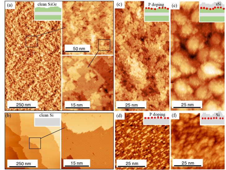
Fig. 2 (a) shows STM images of a SiGe(100) surface prepared by our ex-situ chemical process followed by UHV annealing at T650 ∘C for 15 s. For contrast, Fig. 2 (b) shows images of pure Si(100) surfaces prepared by annealing at 1200 ∘C for 10 s, yielding a characteristic step-terrace structure with the 21/12 reconstruction.
Our lower-temperature process produces surfaces that show no definitive indication of any step-terrace order in larger areas, Fig. 2 (a), but higher magnification images (insets) reveal that the surface is simply rough at the atomic-layer scale with terraces only several nanometers wide. The terraces have mixed p() and c() reconstructions characteristic for SiGe and pure Ge Scappucci et al. (2009). The atomic-layer roughness is most likely caused by the chemical preparations, and the subsequent anneal is inadequate to activate surface smoothing. Roughness at the atomic-layer scale does not cause problems for atomically-precise donor fabrication. Recently, McKibbin et al. have demonstrated entirely functional atomically-precise donor devices on similarly rough epitaxial Si surfaces McKibbin et al. (2009, 2013).
Atomic-layer doping is introduced by exposing the sample to PH3 at 2 Torr for 5 mins (6 Langmuir dose) at room temperature. A T400 ∘C/30 s anneal is used to incorporate P into lattice sites in the surface Ruess et al. (2004); Shen et al. (2004); Lu et al. (2009); Lee et al. (2013); Klesse et al. (2013). Fig. 2 (c) shows the surface after the incorporation anneal, which again is not hot enough to activate surface smoothing, leaving the characteristic atomic-layer roughness on the surface. For comparison, Fig. 2 (d) shows an image of a relaxed bulk Si surface after a similar doping procedure. The surface is covered by monolayers of atomic-height islands formed by Si ejected onto the surface by P incorporation Ruess et al. (2004). We do not observe similar islands on the SiGe surface most likely because ejected Si or Ge is able to migrate to dense preexisting atomic steps, preventing island nucleation.
After P incorporation, samples are capped with 10 to 20 nm thick epitaxial s-Si grown at Å/s at T250 ∘C. Previous reports for Si and Ge structures indicate that this temperature is sufficiently low to inhibit P surface segregation, while yielding a crystalline capping layer Oberbeck et al. (2002). Fig. 2 (e) shows an STM image of the surface of the capping layer, which is rough owing to the relatively low growth temperature. Under similar growth conditions, similarly rough surfaces are reported for both Si and Ge epitaxy Ruess et al. (2004); Scappucci et al. (2009). Fig. 2 (f) shows an example of an STM image of the typical surface topography of a capping layer on pure bulk Si.
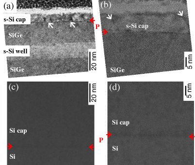
Although there is no clear indication of crystal order, e.g. the 2 reconstruction, in the STM images of the epitaxial s-Si cap, cross-sectional transmission electron microscopy (TEM), Fig. 3, shows that the films are epitaxial. Figs. 3 (a) and (b) show that the SiGe layer structure is preserved with no evidence of threading dislocations in the field of view. Stacking faults are visible in the s-Si cap on the SiGe material. Figs. 3 (c) and (d) show cross-sectional TEM of the relaxed bulk Si:P structure for comparison. There are no stacking faults in the relaxed Si:P structure.
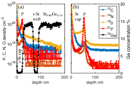
Secondary ion mass spectroscopy (SIMS), Fig. 4 (a), shows that our recipe yields a sharply peaked, FWHM 3 nm, P sheet density cm-2. This is very similar to the FWHM3 nm peaked P sheet density 1.3 cm-2, measured in our Si:P structure, Fig. 4 (b), and consistent with results reported previously Oberbeck et al. (2002). The apparent 3-nm-spread of the dopant peak is due to the limited SIMS depth resolution (4 nm/decade of P density). The SiGe epitaxial cap has substantial backgrounds of N,C, and O contamination, which are somewhat higher than in the bulk Si:P structure, indicating that the lower-temperature process leaves more residual contamination, which may be the cause of the stacking faults in the s-Si capping layer Finch et al. (1963).
III Electronic device characterization
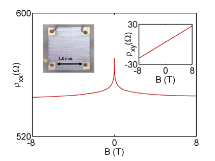
Electronic figures-of-merit for the atomic-layer doping are the electron density and mobility. These are measured using a Hall effect device fabricated on a 1 mm2 die with Al contact pads. Fig. 5 inset shows a photograph of the completed device.
Transport measurements are done in a 3He system with a base temperature of 0.3 K. We use standard lock-in measurement techniques with an excitation current of 100 nA. Hall effect measurements, Fig. 5 inset, yield R , and an electron density n cm-2 and mobility cm2V-1s-1. These values are similar to those reported for atomic-layer doping in Si (1.7-2.4 cm-2 and 30-120 cm2V-1s-1), and Ge (61013 cm-2, 30 cm 2V-1s-1) Oberbeck et al. (2002); Goh et al. (2008); Scappucci et al. (2009). These values of mobility also compare well with the calculations of Hwang and Das Sarma describing transport in the donor layers entirely in a semiclassical Drude model Hwang and Sarma (2013).
Magnetotransport measurements, Fig. 5, provide insight into the character of transport. The data is essentially featureless except for a 4 bump at B0 T, indicative of weak localization which is typical of transport via atomic-layer doping in Si and Ge Oberbeck et al. (2002); Goh et al. (2008). The values of , , and the absence of any Shubnikov-de Haas oscillations indicate that electrons move via the atomic-layer doping, and do not significantly populate the nearby higher-mobility buried Si well (20-50 nm distant).
IV Self-consistent simulations
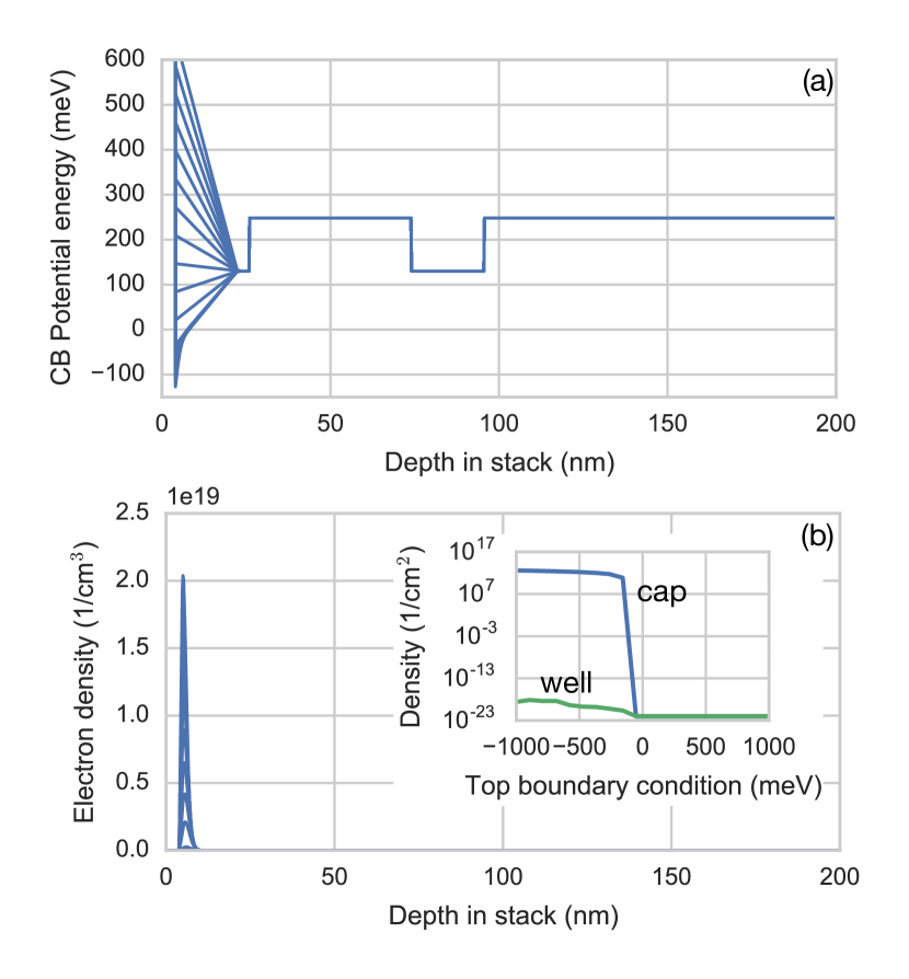
To determine whether electron transport via the 2D phosphorus sheet is physically consistent with the device geometry, we performed self-consistent simulations of the one-dimensional semiconductor heterostructure (along the growth direction). We use the standard predictor-corrector approach to achieve rapidly-convergent calculations Trellakis et al. (1997), assuming zero-field boundary condition at the bottom of the stack, corresponding to charge neutrality deep in the substrate. Since the conduction band is not pinned at the top of the stack (either by a top gate or a high density of surface traps), the appropriate boundary condition is ambiguous. Hence, in our simulations we checked a wide range of Dirichlet boundary conditions at the top to ensure that our conclusions do not rely on particular boundary conditions. Throughout, we work within the Hartree approximation at 4 K, and neglect exchange and correlation effects.
The non-trivial part of the calculation is the proper inclusion of the P-doped layer, which is sufficiently highly doped that typical models of donor neutralization Gao et al. (2013) no longer directly apply. Instead, we explicitly include the , , and four degenerate bands in the 2D density of states model introduced in Ref. Drumm et al., 2012, with the locations of the P-layer bands specified by Ref. Carter et al., 2009. As pointed out in Ref. Drumm et al., 2012, the simple density of states model alone introduces an inconsistency, in that the Fermi level required to impose charge neutrality is predicted to be (unphysically) above the conduction band edge for 1/4 monolayer P-doping. To achieve the Fermi level location of meV below the conduction band edge, as reported from DFT Drumm et al. (2012), we adopt a uniform multiplicative correction to the density of states of the three P-layer bands. We find they need to be suppressed by . The P-layer is smeared out over a 2 nm vertical window, and its bands are included alongside conduction band accumulation in our self-consistent simulations.
In Fig. 6, we show results of our calculations. As can be anticipated from the experiment, the conduction band is effectively pinned by the P-layer, which is incredibly metallic. Since the charge-neutrality condition imposes that the conduction band is 130 meV above the Fermi level at the P-layer, essentially no accumulation occurs in the quantum well, which must dip below the Fermi level to form a channel. As we discussed above, the top interface is not directly controlled, so we confirm that a wide variety of boundary conditions do do not change the core results. While certain plausible boundary conditions can achieve modest accumulation in the silicon cap, we cannot form a channel in the quantum well.
These results indicate that, given our device geometry, we would expect electron occupation in the 2D phosphorus sheet, but not in the quantum well. Hence, our device simulations provide a consistent picture with our electrical transport measurements.
V Summary
In summary, we have demonstrated a recipe for low-temperature surface preparation and atomic-layer doping of SiGe heterostructures that is compatible with atomic-precision donor nanofabrication, while preserving the strained-layer structure and elastic state. SIMS shows the atomic-layer doping has N cm-2 with a FWHM3 nm, while Hall effect measurements at T0.3 K show that the structure has a sheet resistance R , electron density ncm-2 and mobility cm2V-1s-1. These results indicate that electrons stay localized to the donors owing to the conduction band offset of the s-Si cap wth respect to the SiGe. By contrast, to achieve spontaneous electron transfer from the donors to the well would require capping the donor layer with SiGe, as in Fig. 1 (d). Also while we have demonstrated atomic-layer doping on the relaxed Si0.86Ge0.14 surface, the procedure will work equally well on s-Si surfaces formed by epitaxy on the relaxed SiGe structure Lee et al. (2013, 2014). This is an enabling step toward engineering structures that simultaneously utilize atomic-precision donor nanofabrication and SiGe strained-layer engineering. Our proof-of-concept is on a complete heterostructure with a preprocess peak mobility cm2V-1s-1, although the procedure will work equally on a commercially available relaxed SiGe virtual substrate. The next step is to demonstrate a complete atomic-precision nanofabrication process using STM hydrogen depassivation lithography to template donor incorporation laterally in-plane to form 3-D atomically abrupt doped nanostructures. Ruess et al. (2004); Shen et al. (2004); Ruess et al. (2007)
Acknowledgements.
We would like to thank Matthew T. Janish and William M. Mook for cross-sectional TEM. Thanks to Stephen M. Carr and Daniel R. Ward for useful discussions and critical reading of this manuscript. This work has been supported by the Division of Materials Sciences and Engineering, Office of Basic Energy Sciences, U.S. Department of Energy (DOE). This work was performed, in part, at the Center for Integrated Nanotechnologies, an Office of Science User Facility operated for the U.S. Department of Energy (DOE) Office of Science. Sandia National Laboratories is a multimission laboratory managed and operated by National Technology and Engineering Solutions of Sandia, LLC., a wholly owned subsidiary of Honeywell International, Inc., for the U.S. Department of Energy’s National Nuclear Security Administration under contract DE-NA-0003525. The work at NTU has been supported by the Ministry of Science and Technology (103-2112-M-002-002-MY3 and 105-2622-8-002-001) and National Applied Research Laboratories through I-Dream project (05105A2120).References
- Ruess et al. (2004) F. J. Ruess, L. Oberbeck, M. Simmons, K. Goh, A. Hamilton, T. Hallam, S. R. Schofield, N. J. Curson, and R. G. Clark, Nano Lett. 4, 1969 (2004).
- Shen et al. (2004) T.-C. Shen, J. S. Kline, T. Schenkel, S. J. Robinson, J.-Y. Ji, C. Yang, R.-R. Du, and J. R. Tucker, J. Vac. Sci. Technol. B 22, 3182 (2004).
- Ruess et al. (2007) F. J. Ruess , W. Pok, T. C. Reusch, M. Butcher, K. E. Goh, L. Oberbeck, G. Scappucci, A. Hamilton, and M. Simmons, Small 3, 563 (2007).
- Fuechsle et al. (2012) M. Fuechsle, J. A. Miwa, S. Mahapatra, H. Ryu, S. Lee, O. Warschkow, L. C. Hollenberg, G. Klimeck, and M. Y. Simmons, Nat. Nanotech. 7, 242 (2012).
- Scappucci et al. (2009) G. Scappucci, G. Capellini, W. C. T. Lee, and M. Y. Simmons, Appl. Phys. Lett. 94, 162106 (2009).
- Scappucci et al. (2011) G. Scappucci, G. Capellini, B. Johnston, W. M. Klesse, J. A. Miwa, and M. Y. Simmons, Nano Lett. 11, 2272 (2011).
- Zwanenburg et al. (2013) F. A. Zwanenburg, A. S. Dzurak, A. Morello, M. Y. Simmons, L. C. L. Hollenberg, G. Klimeck, S. Rogge, S. N. Coppersmith, and M. A. Eriksson, Rev. Mod. Phys. 85, 961 (2013).
- Kane (1998) B. E. Kane, Nature 393, 133 (1998).
- Vrijen et al. (2000) R. Vrijen, E. Yablonovitch, K. Wang, H. W. Jiang, A. Balandin, V. Roychowdhury, T. Mor, and D. DiVincenzo, Phys. Rev. A 62, 012306 (2000).
- Fang et al. (2005) A. Fang, Y.-C. Chang, and J. R. Tucker, Phys. Rev. B 72, 075355 (2005).
- Hollenberg et al. (2006) L. C. L. Hollenberg, A. D. Greentree, A. G. Fowler, and C. J. Wellard, Phys. Rev. B 74, 045311 (2006).
- Hill et al. (2015) C. D. Hill, E. Peretz, S. J. Hile, M. G. House, M. Fuechsle, S. Rogge, M. Y. Simmons, and L. C. L. Hollenberg, Sci. Adv. 1, e1500707 (2015).
- Koiller et al. (2001) B. Koiller, X. Hu, and S. Das Sarma, Phys. Rev. Lett. 88, 027903 (2001).
- Gamble et al. (2015) J. K. Gamble, N. T. Jacobson, E. Nielsen, A. D. Baczewski, J. E. Moussa, I. Montaño, and R. P. Muller, Phys. Rev. B 91, 235318 (2015).
- Koenraad and Flatté (2011) P. Koenraad and M. E. Flatté, Nat. Mater. 10, 91 (2011).
- Pok et al. (2007) W. Pok, T. C. Reusch, G. Scappucci, F. J. Rueb, A. R. Hamilton, and M. Y. Simmons, IEEE Trans. Nanotechnol. 6, 213 (2007).
- Weber et al. (2014) B. Weber, H. Ryu, Y.-H. M. Tan, G. Klimeck, and M. Y. Simmons, Physical Review Letters 113, 246802 (2014).
- Scrymgeour et al. (2017) D. Scrymgeour, A. Baca, K. Fishgrab, R. Simonson, M. Marshall, E. Bussmann, C. Nakakura, M. Anderson, and S. Misra, Applied Surface Science 423, 1097 (2017).
- Gramse et al. (2017) G. Gramse, A. Kölker, T. Lim, T. J. Stock, H. Solanki, S. R. Schofield, E. Brinciotti, G. Aeppli, F. Kienberger, and N. J. Curson, Science Advances 3, e1602586 (2017).
- Scappucci et al. (2007) G. Scappucci, F. Ratto, D. Thompson, T. Reusch, W. Pok, F. Rueß, F. Rosei, and M. Simmons, Appl. Phys. Lett. 91, 222109 (2007).
- Fuechsle et al. (2007) M. Fuechsle, F. J. Rueß, T. C. Reusch, M. Mitic, and M. Y. Simmons, J. Vac. Sci. and Technol. B 25, 2562 (2007).
- Lee et al. (2010) W. Lee, G. Scappucci, D. Thompson, and M. Simmons, Appl. Phys. Lett. 96, 043116 (2010).
- Goh et al. (2008) K. E. J. Goh, Y. Augarten, L. Oberbeck, and M. Y. Simmons, Appl. Phys. Lett. 93, 142105 (2008).
- Sullivan et al. (2004) D. F. Sullivan, B. E. Kane, and P. E. Thompson, Appl. Phys. Lett. 85, 6362 (2004).
- Keizer et al. (2015) J. G. Keizer, S. Koelling, P. M. Koenraad, and M. Simmons, ACS Nano 9, 12537 (2015).
- Lee et al. (2005) M. L. Lee, E. A. Fitzgerald, M. T. Bulsara, M. T. Currie, and A. Lochtefeld, J. Appl. Phys. 97, 011101 (2005).
- Friesen et al. (2003) M. Friesen, P. Rugheimer, D. E. Savage, M. G. Lagally, D. W. van der Weide, R. Joynt, and M. A. Eriksson, Phys. Rev. B 67, 121301 (2003).
- Pudalov et al. (1993) V. M. Pudalov, M. D’Iorio, S. V. Kravchenko, and J. W. Campbell, Phys. Rev. Lett. 70, 1866 (1993).
- Kim et al. (2017) J.-S. Kim, A. M. Tyryshkin, and S. A. Lyon, Applied Physics Letters 110, 123505 (2017).
- Lai et al. (2005) K. Lai, W. Pan, D. C. Tsui, S. A. Lyon, M. Mühlberger, and F. Schäffler, Phys. Rev. B 72, 081313 (2005).
- Lu et al. (2009) T. M. Lu, D. C. Tsui, C.-H. Lee, and C. W. Liu, Appl. Phys. Lett. 94, 182102 (2009).
- Laroche et al. (2015) D. Laroche, S.-H. Huang, E. Nielsen, Y. Chuang, J.-Y. Li, C. W. Liu, and T. M. Lu, AIP Adv. 5, 107106 (2015).
- Mi et al. (2015) X. Mi, T. M. Hazard, C. Payette, K. Wang, D. M. Zajac, J. V. Cady, and J. R. Petta, Phys. Rev. B 92, 035304 (2015).
- Zajac et al. (2015) D. Zajac, T. Hazard, X. Mi, K. Wang, and J. Petta, Applied Physics Letters 106, 223507 (2015).
- Klauk et al. (1996) H. Klauk, T. N. Jackson, S. F. Nelson, and J. O. Chu, Applied Physics Letters 68, 1975 (1996), http://dx.doi.org/10.1063/1.115644 .
- Oberbeck et al. (2002) L. Oberbeck, N. Curson, M. Simmons, R. Brenner, A. Hamilton, S. Schofield, and R. Clark, Appl. Phys. Lett. 81, 3197 (2002).
- Lee et al. (2013) W. Lee, N. Bishop, D. Thompson, K. Xue, G. Scappucci, J. Cederberg, J. Gray, S. Han, G. Celler, M. Carroll, et al., Appl. Surf. Sci. 265, 833 (2013).
- Lee et al. (2014) W. Lee, S. McKibbin, D. Thompson, K. Xue, G. Scappucci, N. Bishop, G. Celler, M. Carroll, and M. Simmons, Nanotechnology 25, 145302 (2014).
- Klesse et al. (2013) W. M. Klesse, G. Scappucci, G. Capellini, J. M. Hartmann, and M. Y. Simmons, Appl. Phys. Lett. 102, 151103 (2013).
- Ishizaka and Shiraki (1986) A. Ishizaka and Y. Shiraki, J. Electrochem. Soc.Journal of the Electrochemical Society 133, 666 (1986).
- Okumura et al. (1998) H. Okumura, T. Akane, and S. Matsumoto, Appl. Surf. Sci. 125, 125 (1998).
- Tersoff et al. (1995) J. Tersoff, Y. Phang, Z. Zhang, and M. Lagally, Phys. Rev. Lett. 75, 2730 (1995).
- McKibbin et al. (2009) S. McKibbin, W. Clarke, A. Fuhrer, T. Reusch, and M. Simmons, Appl. Phys. Lett. 95, 233111 (2009).
- McKibbin et al. (2013) S. McKibbin, G. Scappucci, W. Pok, and M. Simmons, Nanotechnology 24, 045303 (2013).
- Finch et al. (1963) R. H. Finch, H. J. Queisser, G. Thomas, and J. Washburn, Journal of Applied Physics 34, 406 (1963), http://dx.doi.org/10.1063/1.1702622 .
- Hwang and Sarma (2013) E. Hwang and S. D. Sarma, Phys. Rev. B 87, 125411 (2013).
- Carter et al. (2009) D. J. Carter, O. Warschkow, N. A. Marks, and D. R. McKenzie, Phys. Rev. B 79, 033204 (2009).
- Trellakis et al. (1997) A. Trellakis, A. Galick, A. Pacelli, and U. Ravaioli, J. Appl. Phys. 81, 7880 (1997).
- Gao et al. (2013) X. Gao, E. Nielsen, R. P. Muller, R. W. Young, A. G. Salinger, N. C. Bishop, M. P. Lilly, and M. S. Carroll, J. Appl. Phys. 114, 164302 (2013).
- Drumm et al. (2012) D. W. Drumm, L. C. Hollenberg, M. Y. Simmons, and M. Friesen, Phys. Rev. B 85, 155419 (2012).