Magnetic-field-assisted transmission of THz waves through a graphene layer combined with a periodically perforated metallic film
Abstract
We consider a graphene sheet encapsulated in a two-dimensional metallic grating and a substrate () and subjected to an external magnetic field (in Faraday configuration). The grating consists of a thin perfectly conducting metal film perforated with a 2D periodic array of square holes. According to our calculations, significant changes in the spectra of the Faraday rotation angle of the transmitted wave and of the magnetic circular dichroism should be expected in this situation compared to bare graphene. We explain this enhancement by the excitation of graphene magnetoplasmons that accompanies the transmission of the electromagnetic wave through the structure. The results can be interesting for applications in THz photonics, such as switchable rotating polarizer and optical isolator.
I Introduction
One of the prominent features of the magnetoactive structures is a strong dependence of the electromagnetic wave characteristics upon the direction of propagation. An illustrative example is the Faraday effect Faraday (1846), where the direction of the rotation of the plane of polarization is different for the forward- and backward-proparating waves in magnetoactive media along the direction of static external magnetic field (Faraday geometry). Similar phenomenon – nonreciprocal phase shiftGabriel and Brodwin (1965); Auracher and Witte (1975) – takes place in asymmetric structures Dötsch et al. (2005)(e.g., waveguides) when the direction of propagation is perpendicular to the magnetic field (Voigt geometry). These phenomena consitute the basis for the operation principles of a variety of microwave photonic devices, such as optical isolatorsAplet and Carson (1964); Jalas et al. (2013), circulators Ribbens (1965); Takei and Mizumoto (2010), and switches Tien et al. (1974); Ishida et al. (2016) (for a review on practical application of magnetooptical materials see Shoji and Mizumoto (2014); Shoji et al. (2016)).
The general tendency to the minituarization of the photonic components resulted in the creation of magnetoptical devices, which key building blocks are photonic crystalsQiu et al. (2011); Śmigaj et al. (2010); Dmitriev and Kawakatsu (2012); Wang and Fan (2005); Zhang et al. (2013); Fan et al. (2011); Wang et al. (2009); Fan et al. (2012) or electromagnetic metasurfaces Chen et al. (2015a, b). Yet, the diffraction limit of electromagnetic waves imposes one of the fundamental obstacles for further minituarization and growth of integration of photonic devices in opto-electronics circuitry. One of the possible ways to circumvent this limit is to build the photonic components, whose operation principles are based on the surface electromagnetic waves instead of on their free space counterparts. To be specific, incorporating metallic structures into a photonic platform allows one to create circuitry, operating on surface plasmon-polaritons – a special kind of the electromagnetic waves, whose energy is localized near the metal-dielectric interface and whose wavelength is considerably smaller than that of the free space wave with the same frequency Ozbay (2006); Stockman (2011).
Combining plasmonics with magnetooptics Temnov (2012); Armelles et al. (2013)gives a variety of advantagesMaksymov (2015). First, magnetic field allows to achieve the dynamical tunability (control of parameters in real time) of plasmonic structureChiu and Quinn (1972); Temnov et al. (2010); Fan et al. (2013, 2016). Secondly, the aforementioned phenomenon of the nonreciprocal propagation allows to create plasmonic analogues of different magnetooptical devices Firby and Elezzabi (2015); Davoyan and Engheta (2013); Firby and Elezzabi (2016). Third, the resonant excitation of the magnetoplasmons and their coupling to the transmitted and reflected bulk waves results in a significant enhancement of the Faraday and magnetooptical Kerr effects Chin et al. (2013); Caballero et al. (2015); Belotelov et al. (2011); Kreilkamp et al. (2013). However, introducing the magnetooptical materials into the plasmonic circuitry enhances significantly the losses in the system, thus reducing the free path of magnetoplasmons (compared to the conventional plasmonic structures). As a result, nowadays there is a huge demand for novel magnetoplasmonic materials.
In the context discussed above, graphene emerges as a promising candidate, operating the THz and mid-IR spectral range. This material possesses several properties, which can be advantageous for the magnetooptics and magnetoplasmonics. To begin with, surface plasmon-polaritons in graphene Xiao et al. (2016); García de Abajo (2014); Chen et al. (2017); Bludov et al. (2013); Low and Avouris (2014)are characterized by both large lifetime and high degree of field confinement Koppens et al. (2011); Nikitin et al. (2011). Simultaneously, graphene is a magnetoactive material: being subjected to an external static magnetic field (perpendicular to its surface), graphene exhibits some unusual magnetic properties, like the Hall effect at room tempertureNovoselov et al. (2005); Zhang et al. (2005). Furthermore, its conductivity (and, consequently, its transmittance and the reflectanceTamagnone et al. (2014, 2016); Shimano et al. (2013); Crassee et al. (2010); Sounas et al. (2013) as well as the dispersion properties of magnetoplasmons Berman et al. (2008); Roldán et al. (2009); Crassee et al. (2012); Yan et al. (2012)) can be effectively tuned by changing the applied magnetic field. The possibility to achieve the magnetoplasmon-mediated enhancement of the magnetooptical phenomena was demonstrated in various graphene-based structures, such as a periodic array of graphene ribbons Tymchenko et al. (2013), a graphene monolayer patterned with the periodical antidot array Poumirol et al. (2017), an array of graphene-covered nanowires Kuzmin et al. (2016), or a monolayer graphene metasurface Fallahi and Perruisseau-Carrier (2012).
In this paper we study the interaction of THz electromagnetic wave with a graphene monolayer cladded by a semi-infinite substrate and a periodically perforated metallic film of finite thickness. This metallic film is assumed made of a perfect metal and containing a two-dimensional (2D) periodic array of square holes. The structure is subjected to an external magnetic field directed perpendicularly to the surface (Faraday geometry). We demonstrate that if the two-dimensional metallic grating is sparse enough, it screens the incident long-wavelength electromagnetic wave. As a result, in the low-frequency range the Faraday rotation in the graphene covered with the perforated metal film is less than that in the graphene layer alone. At high frequencies, the sparse metallic grating almost does not influence the propagation of the electromagnetic wave. At the same time, in the intermetiate frequency range the diffraction of the incident electromagnetic wave on the grating results in the excitation of graphene magnetoplasmons. This process increases considerably the Faraday rotation angle of the polarization vector for a linearly polarized wave. For a circularly polarized propagating wave, the presence of the perforated metallic film leads to inversion of the sign of the magnetic circular dichroism (MCD) in the low-frequency range.
The paper is organized as follows. In Sec.II we obtain the principal equations governing the process of incident wave diffraction on graphene combined with the periodical array of holes in the metal film. Section III is devoted to a detailed discussion of how the parameters of this structure influence the Faraday rotation angle of the transmitted electromagnetic wave. In Sec. IV we investigate the magnetic circular dichroism in this structure. The conclusions are presented in Sec.V.
II Diffraction of plane electromagnetic wave on metal film with periodic array of holes
We consider a perfectly conducting metal film of thickness (whose film surfaces are situated at planes , see Fig.1), containing a periodic array of square holes, each of width , arranged at , and forming a square lattice. Here is the period of the square lattice and , are the hole indices. We also assume that this metallic grating is deposited on top of a graphene monolayer, arranged at the plane . The graphene monolayer is deposited on top of a semi-infinite dielectric substrate () occupying the half-space and characterized by the dielectric function . The plane wave impinges on the metal grating from air (the half-space ) at normal incidence.
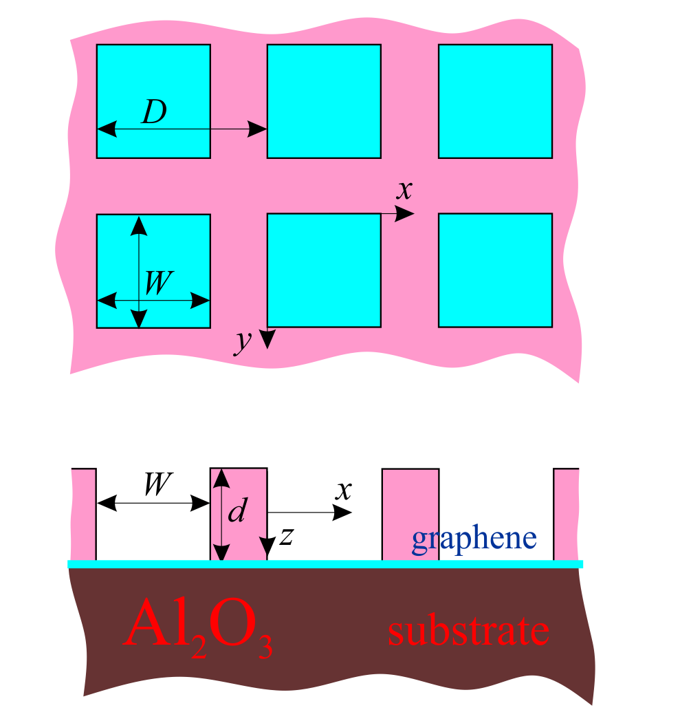
The periodicity of the structure in the directions and , as well as the normal incidence of the external wave impose the requirement for the solution of Maxwell equations to be also periodic. In half-spaces and (vacuum and substrate) electromagnetic fields can be represented in the form of Fourier series with respect to the lattice vector , namely
where stand for the indices of spatial harmonics, and is the 2D wavevector in the transverse plane . In Eqs. (II) and (II) the electromagnetic field time-dependence is implicitly assumed as . Also
is the 22 unit matrix and
is the Pauli matrix,
and are -components of the wavevector, corresponding to harmonics in the vacuum and substrate, respectively.
Equations (II) and (II) can be interpreted in the following manner. In the half-space , occupied by air, the total electromagnetic field is composed of the electromagnetic fields, which correspond to incident [first term in Eq.(II)] and reflected [second term in Eq.(II)] waves. At the same time, in the substrate (half-space ) electromagnetic field [see Eq. (II)] contains the transmitted wave only. If the sign of the wavevector’s -component (where ) satisfies the conditions , , the transverse incident wave propagates along -axis in the positive direction and is characterized by the wavevector and the magnetic field amplitude . The reflected and transmitted waves contain an infinite number of spatial harmonics. The reflected wave harmonic with index [characterized by the amplitude and 3D wavevector ] in the negative direction of -axis can be either propagating wave (in this case and will be purely real and positive) or evanescent (in this case and will be purely imaginary and positive). Owing to the fact that substrate’s dielectric constant is complex, each of the transmitted wave harmonics [with amplitude and 3D wavevector ] is of mixed type: along axis it propagates in its positive direction with exponential factor , but having a decaying amplitude .
Inside the holes in the metallic film, for , ,, transverse components of the magnetic and electric fields can be represented in matrix form as (see Appendix A for details)
| (36) | |||||
| (44) | |||||
where the matrices
and are the mode indices, , are the amplitudes of E-modes, while , are the H-modes amplitudes. In general, E-modes inside the square hole exist for nonzero mode indices – this is taken into account in Eqs. (36) and (44) introducing the factor in front of the E-mode coefficients (where and is the Kronecker delta). On the other hand, the H-mode index ( or ) can be zero – excepting the case when both indices , and this term is implicitly excluded from the summation in Eqs. (36) and (44). Notice, that Eqs. (36) and (44) satisfy the boundary conditions, namely, zero tangential components of the electric field and zero normal components of the magnetic field on the metal surfaces, , , , . Along with this, the periodicity of the solutions of Eqs. (36) and (44) is achieved through the independence of the mode amplitudes upon the hole indices .
Applying the boundary conditions (continuity of the tangential components of the electric and magnetic fields) at the surface of the metal film , where graphene is absent, results in the following system of equations:
| (52) | |||
| (57) | |||
| (62) | |||
| (69) |
Boundary conditions across the graphene sheet (at ) imply the continuity of the electric field tangential components and discontinuity of the tangential components of the magnetic field due to the presence of the currents in graphene, namely:
| (70) | |||
| (71) | |||
| (72) | |||
| (73) |
where
are the components of the graphene conductivity tensor in magnetic fieldFerreira et al. (2011),
In the above relations are energy levels of the graphene in external magnetic field, m/s is the Fermi velocity in graphene, is the magnetic length, is the so-called ac universal conductivity of graphene,
is the Fermi-Dirac distribution function, is the Fermi energy, and is the electron relaxation rate in graphene.
Combining Eqs. (83) with (II), it is possible to obtain the following expressions for the electromagnetic field at the metal film surface (),
Similar to Eqs.(52) and (69) we can write:
| (90) | |||
| (95) | |||
| (98) | |||
| (105) |
Multiplying Eqs. (52) and (90) by and integrating over the area of the hole , , we obtain
| (110) | |||
| (113) | |||
| (116) | |||
| (119) | |||
| (122) | |||
| (123) | |||
| (126) |
where
and , . While obtaining Eqs. (113) and (123), we have used the orthogonality of trigonometric functions for ,
Also we multiply Eqs. (69) and (105) by , and integrate over the area of one period of the structure , , and after taking into account orthogonality of the plane waves in the unit cell,
we obtain
| (132) | |||
| (133) | |||
| (136) | |||
| (139) | |||
| (142) |
where
and the overbar stands for the complex conjugation. Thus, solving the linear system of Eqs. (113) – (139), it is possible to obtain the amplitudes of the excited modes inside the holes as well as amplitudes of the reflected and transmitted harmonics. From these it is possible to calculate the total reflectance and transmittace of the structure as [see Applendix A for details]
| (149) | |||||
| (155) | |||||
It is common to characterize the transmission of graphene-based structures in terms of the so called extinction relative to bare graphene with zero Fermi energy (designated by the abbreviation CNP that stands for ”charge neutrality point”)Poumirol et al. (2017), , where both transmittances can be calculated using the above equation. We shall present this quantity calculated in the subsequent sections.
III Faraday rotation
One of the principal goals of the present work is to investigate the influence of the magnetoplasmon resonance on the Faraday rotation of an electromagnetic wave traversing the graphene layer. In order to clarify the role of magnetoplasmons in the Faraday rotation, we start this section by briefly considering the dispersion properties of magnetoplasmons.
III.1 Magnetoplasmons in graphene
The dispersion relation of magnetoplasmons can be obtained from the following equation (see Applendix B.1 for details):
| (156) | |||
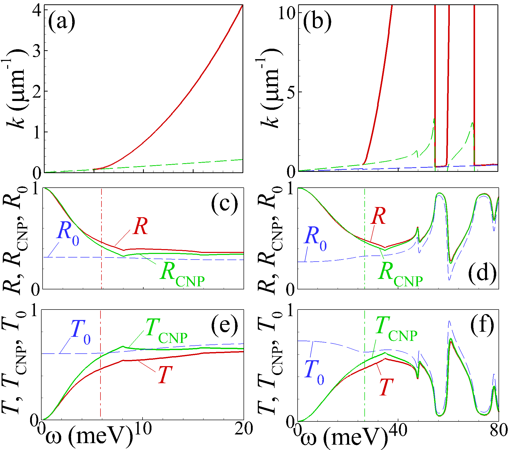
where , and, similar to the previous section we require , (). If we suppose that both the substrate and the graphene layer are lossless [, ], then the dispersion relation (156) possesses a solution in terms of purely real frequency and wavevector . The magnetoplasmon dispersion is depicted in Figs. 2(a) and 2(b) for low and high magnetic fields, respectively. When the external perpendicular magnetic field is applied to graphene, the magnetoplasmon spectrum contains a low-frequency gap and the magnetoplasmons exist at frequencies higher than a threshold frequency (which is approximately equal to the cyclotron frequency, ) and for the wavevectors larger than the corresponding threshold wavevector . At the threshold frequency, which is equal to in Fig. 2(a) and in Fig. 2(b), the magnetoplasmon spectrum splits off from the substrate light line, , depicted by green dashed lines. Consequently, the value of the wavevector threshold is ). For higher frequencies, the magnetoplasmon spectrum lies above the light line in the substrate and it results in purely imaginary and , which determine the localization of the electromagnetic field of the magnetoplasmon close to the graphene layer. Notice that the real part of the substrate dielectric constant is positive [], in this low-frequency range . The physical reason for the existence of magnetoplasmons is the coupling of the electromagnetic wave with excitations of free charge-carriers in graphene.
It is important to notice that in the frequency ranges and [inside the limits of the horizontal axis of Fig.2(b)] the real part of the substrate dielectric constant is negative [] owing to the excitations of optical phonons.111The substrate dielectric function includes optical phonon response, (157) where , meV, meV, meV, meV are phonon frequencies, meV, meV, meV, meV are the phonon dampings, and , , , are the weighting coefficients. Consequently, in these frequency ranges the physical reason for the existence of surface waves is somewhat different since the substrate-air interface is able to sustain surface modes due to coupling of the electromagnetic wave to the substrate phonons rather than because of the interaction with the free electron oscillations in graphene (in the following these modes will be referred to as surface phonon-polaritons). In this case the polariton dispersion curve lies above the light line in vacuum [blue dashed lines in Fig.2(b)].
III.2 Magnetoplasmon-enhanced Faraday rotation
The mismatch between the wavevectors of magnetoplasmons and the light line (either in the substrate or in air) determines the impossibility to excite magnetoplasmons by a propagating electromagnetic wave, falling directly onto the graphene layer. One way to overcome this wavevector mismatch is to use the electromagnetic wave diffraction on some kind of periodic structure added to the graphene layer. In this case the electromagnetic wave diffraction on the periodic structure gives rise to a variety of harmonics [in Eqs. (II) and (II) their 2D wavevectors are ]. If at a certain frequency the wavevector of one of them coincides with that of the magnetoplasmon spectrum (156), then the energy of the external electromagnetic wave can be effectively transferred into the energy of the excited magnetoplasmon.
It can be understood from Figs. 2(c) – 2(f), that the presence of the perforated metal film on top of the graphene layer modifies significantly the reflectance and transmittance of the structure both in the case of doped (solid red lines) and undoped (solid green lines) graphene. The incident wave is considered to be linearly polarized with the magnetic field along the -axis (i.e. , ). For the parameters of Figs. 2(c) and 2(e) the lattice vector is equal to , for which the predicted frequency of the magnetoplasmon resonance [for see Fig. 2(a)] is . Similarly, for the parameters of Figs. 2(d) and 2(f) the lattice vector is and the magnetoplasmon resonance frequency is [which can be obtained from Fig. 2(b)]. In the low frequency range, , the wavelength of the incident electromagnetic wave exceeds significantly the period of the grating, . As a result, the perforated metal film screens the incident wave almost like a continuous metal as evidenced by the enhanced reflectance of the structure, [see Figs. 2(c) and 2(d)] and its suppressed transmittance, [see Figs. 2(e) and 2(f)], as compared to the reflectance, and transmittance, of bare graphene [dashed blue lines in Figs. 2(c)–2(f)] 222The expressions for and as well as the details of derivation can be found in Appendix B.2.. In the high-frequency range, , the situation is opposite, namely, the wavelength of the incident electromagnetic wave is considerably shorter than the period of structure, , and, of course, also smaller than the hole width, . In this case the metal film almost does not influence the propagation of the electromagnetic wave, hence the reflectance, , and the transmittace, , of graphene with perforated metal film almost conside with those of bare graphene ( and ).
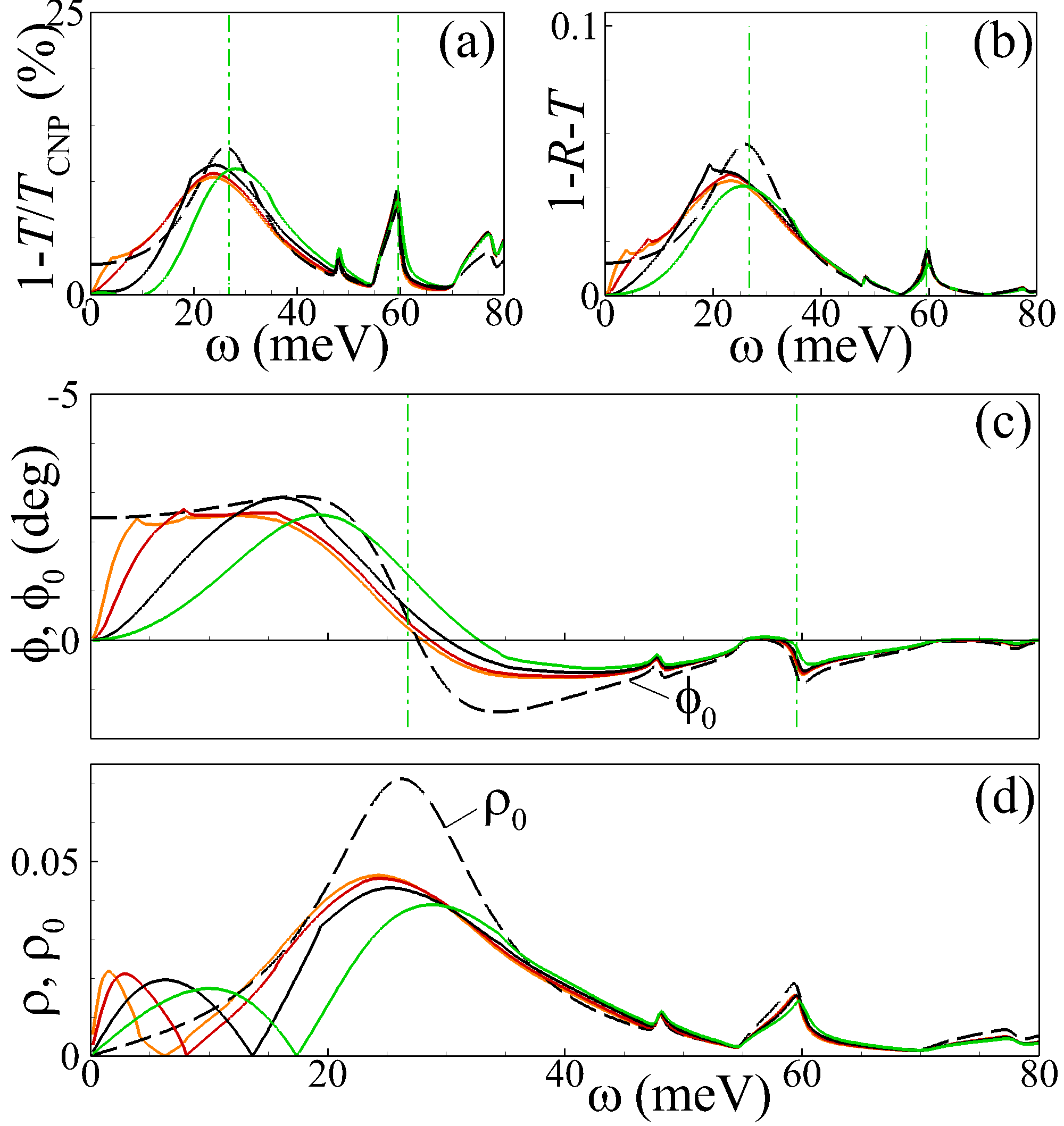
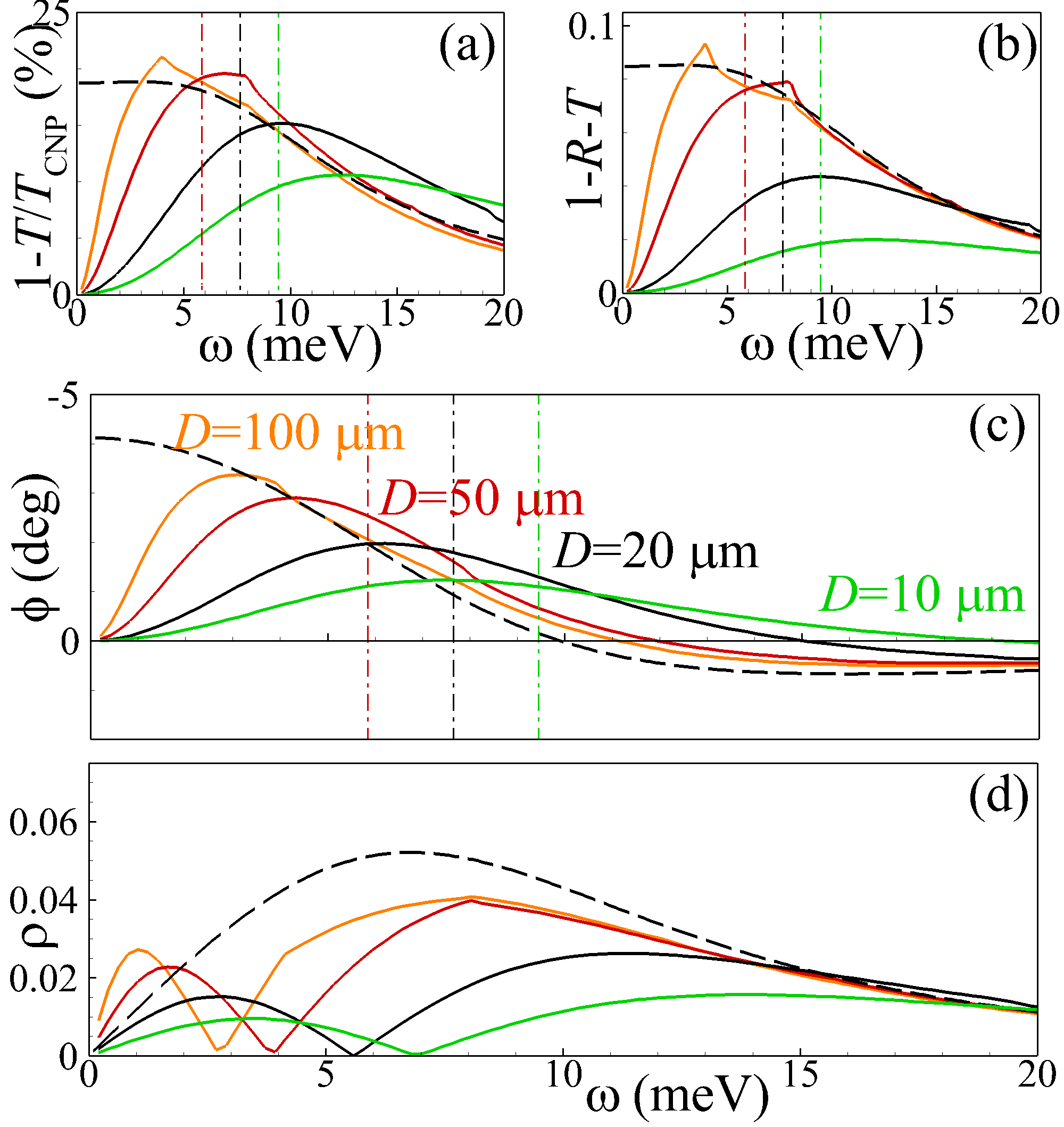
The most interesting situation takes place in the intermediate frequency range, when the frequency of the incident wave is close to the magnetoplasmon resonance frequency . As it can be seen from Figs. 2(e) and 2(f), it is in this frequency range that the maximal deviation between the transmittance of the perforated metal film with doped graphene () and that of the same structure with undoped graphene () takes place owing to the the excitation of magnetoplasmons. This phenomenon is shown in Figs. 3(a) and 4(a). Near the frequency of magnetoplasmon resonance, (depicted by vertical dash-and-dotted lines), the extinction attains its local maximum, as does the absorbance, [see Figs. 3(b) and 4(b)]. Interestingly, both the extinction and the absorbance attain their maxima in the structures that do not allow for the excitation of magnetoplasmons. Such a situation can take place in two kinds of structures: (i) graphene layer without perforated metallic film (dashed black lines in Figs. (3) and (4)); (ii) graphene layer with grating but when the lattice vector of the latter, , is below the threshold (that is, when the period is too large, so that the magnetoplasmon resonance eigenfrequency does not exist) – see the corresponding spectra in Figs. 2(a) and 2(b)]. Examples of such situation can be found for structures with (orange lines) in Figs. 3(a) and 3(b), as well as for (orange lines), (red lines), and (black lines) in Figs. 4(a) and 4(b). Nevertheless, in these cases the extinction and absorbance attain their maxima in the vicinity of the cyclotron frequency owing to the resonant interaction between the electromagnetic wave and graphene’s charge carriers, rotating in the perpendicular magnetic field (in more details this phenomenon will be described in Sec. IV). It should be noticed, that at low magnetic field [Figs. 3(a) and 3(b)] there is a certain descrepancy between the predicted magnetoplasmon resonance and the maxima of absorbance and extinction. The reason for this seems to be the following: the relaxation rate of free carriers in graphene used in the calculation was , i.e., its value is comparable with the predicted frequencies of magnetoplasmon resonance . As a result, the magnetoplasmon oscillations are overdamped in this case. A possible solution of this problem is to shift the magnetoplasmon resonance to the higher-frequency range, e.g., by increasing the external magnetic field strength . In this case the agreement between the predicted magnetoplasmon resonance frequency and the maxima of the absorbance and the extinction is considerably better [see Figs. 4(a) and 4(b)]. At the same time, the maxima in the extinction and absorbance spectra at appear owing to the excitation of the aforementioned surface phonon-polaritons.
How does the excitation of the graphene magnetoplasmons, which manifests itself by the increase of extinction and absorbance, influences the Faraday rotation angle of the transmitted wave? To answer this question we compare the Faraday rotation angle of the electromagnetic wave transmitted through the perforated metal film on top of the doped graphene layer [solid lines in Figs. 3(c) and 4(c)] with that () of the electromagnetic wave passing through bare graphene with the same parameters but without the grating [dashed lines in Figs. 3(c) and 4(c)]. The formulae permitting to calculate the Faraday rotation angle from zero-harmonics amplitudes can be found, e.g., in Ref.Born and Wolf (1999). It is evident that in the low-frequency region, , the rotation angle is considerably below , i.e., the presence of the perforated metal film hampers the Faraday rotation effect. This fact is a consequence of the above-mentioned attenuated transmittance of the perforated metal film, shown in Figs. 2(c) and 2(d). Notice that the decrease of the Faraday rotation angle, (compared to ), in the low-frequency range is accompanied by the enhancement of the ellipticity, , of the transmitted wave polarization (again, compared to the ellipticity of the polarization of the electromagnetic wave transmitted through the bare graphene) – see Figs. 3(d) and 4(d). In the high-frequency range, where , the aforementioned neglible interaction between the electromagnetic wave and perforated metal film [see Figs. 2(c) and 2(d)] reveals into the fact that and . Nevertheless, in the intermediate frequency range, , when the magnetoplasmon resonance eigenfrequency does exist [red, black, and green solid lines in Figs. 3(c) and 3(d), as well as green solid lines in Figs. 4(c) and 4(d)], the ellipticity (so, the transmitted wave polarization becomes closer to the linearly polarized wave), but the Faraday rotation angle satisfies the condition . In other words, excitation of graphene magnetoplasmons owing to the presence of the perforated metal film on top of graphene increases the Faraday rotation angle. In the situation, where the magnetoplasmon resonance eigenfrequency does not exist [, examples are orange solid lines in Figs. 3(c) and 3(d), as well as orange, red, and black solid lines in Figs. 4(c) and 4(d)] the Faraday rotation angle is almost the same as (or even less), even though the ellipticity can be smaller than .
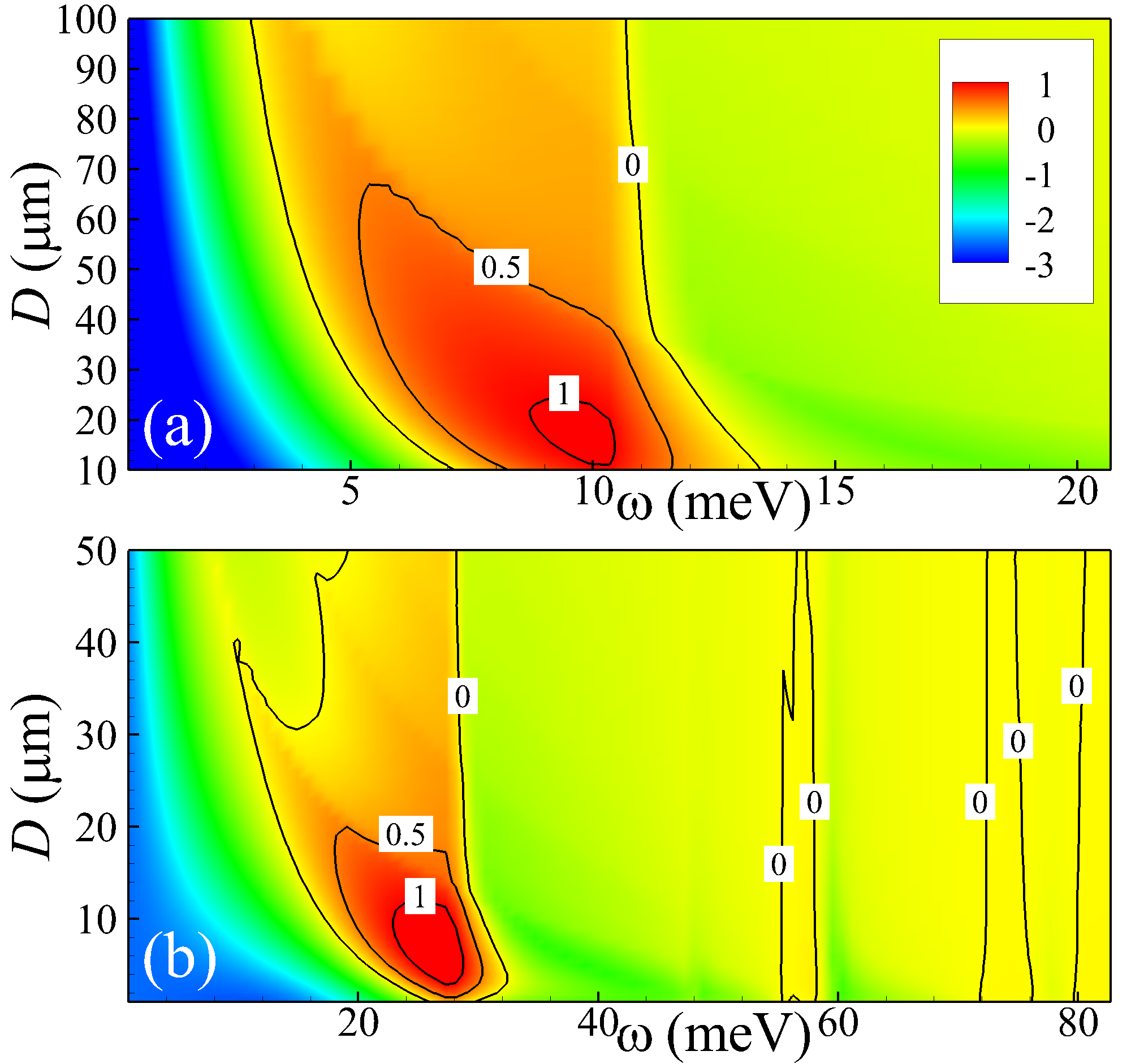
More detailed information of how the presence of the perforated metal film on top of graphene changes the Faraday rotation angle can be extracted from Fig. 5, which demonstrates the dependence of the Faraday angle difference, , upon the frequency and the period of the hole grating . It is clearly seen that in the intermediate frequency range [ in Fig.5(a) and in Fig.5(b)] the Faraday angle difference is positive, , that is, the presence of the perforated metal film increases the absolute value of the Faraday rotation angle as compared to the case without the grating. Beyond this frequency range the Faraday angle difference is mainly negative, .333Excepting narrow frequency windows at , and , where, nevertheless, an increase of the Faraday rotation angle is negligibly small. In other words, both in the low- and in the high-frequency ranges presence of the perforated metal film on top of graphene suppresses the Faraday rotation of transmitted wave. At the same time, inside the intermediate frequency range there exist some optimal values of the hole grating period [in Fig.5(a)] and [in Fig.5(b)], for which the Faraday angle difference is maximal and exceeds .
IV Magnetic circular dichroism
The term dichroism means the property shown by certain materials of having different absorption coefficients for light polarized in different directions.Born and Wolf (1999) If the amplitudes of the transmitted clockwise and anticlockwise polarized waves will not be equal in the presence of a magnetic field applied along their direction of propagation, the material possesses the magnetic circular dichroism (MCD). This is different from the Faraday rotation effect that exists in non-absorbing media. Applying a magnetic field to the dielectric causes the material to exhibit circular birefringence, i.e. the propagation velocities of the clockwise and anticlockwise polarized waves become unequal. The Faraday rotation angle is then proportional to the difference in the refractive indices for two circular polarizations.Basu (1997) Of course, the two effects are interconnected, especially in an intrinsically absorbing plasmonic structure such as the one considered here, but still we can attempt to make a distinction between them. Let us point it out that the system under study has no dichroism in the absence of magnetic field.
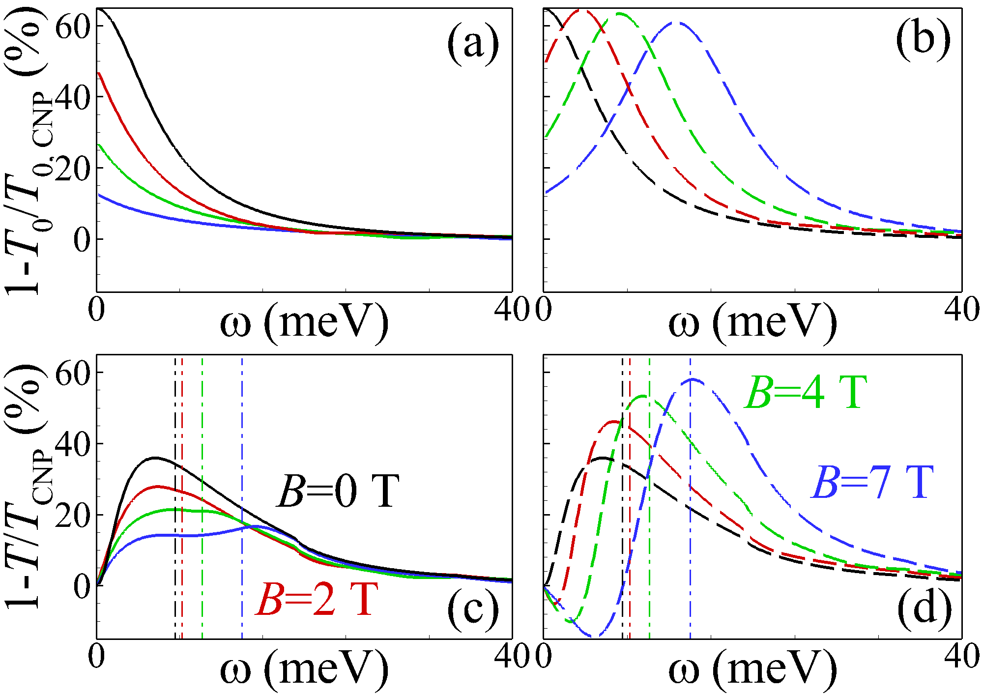
In order to clarify the influence of magnetoplasmons on the MCD of the structure, we consider first the extinction of the clockwise and anticlockwise circularly polarized electromagnetic waves [depicted in Figs. 6(a) and 6(b), respectively], transmitted through the graphene layer without 2D grating on top of it. A clockwise polarized incident wave is characterized by the phase shift between the and components of its magnetic field (), while their amplitudes are equal. The phase shift between the magnetic field components in the anticlockwise circularly polarized incident wave is , i.e. .
As follows from the comparison of Figs. 6(a) and 6(b), at zero magnetic field (black lines) the extinction values of clockwise and anticlockwise circularly polarized electromagnetic waves are equal. When graphene is doped with holes (negative chemical potential ), application of external magnetic field results in the circular MCD: for the same frequency the extinction of the anticlockwise-polarized wave [Fig. 6(b)] exceeds that of the clockwise circularly polarized wave [Fig. 6(a)]. The frequency dependence of the extinction, being a monotonically decreasing function in the case of clockwise-polarized wave, in the case of anticlockwise-polarized wave exhibits its maximum at the cyclotron frequency . As a consequence, the growth of the magnetic field leads to the blue-shift of the maximum of the anticlockwise-polarized wave extinction spectrum [Fig. 6(b)] and to a monotonic decrease of the clockwise-polarized wave extinction [see Fig. 6(a)].
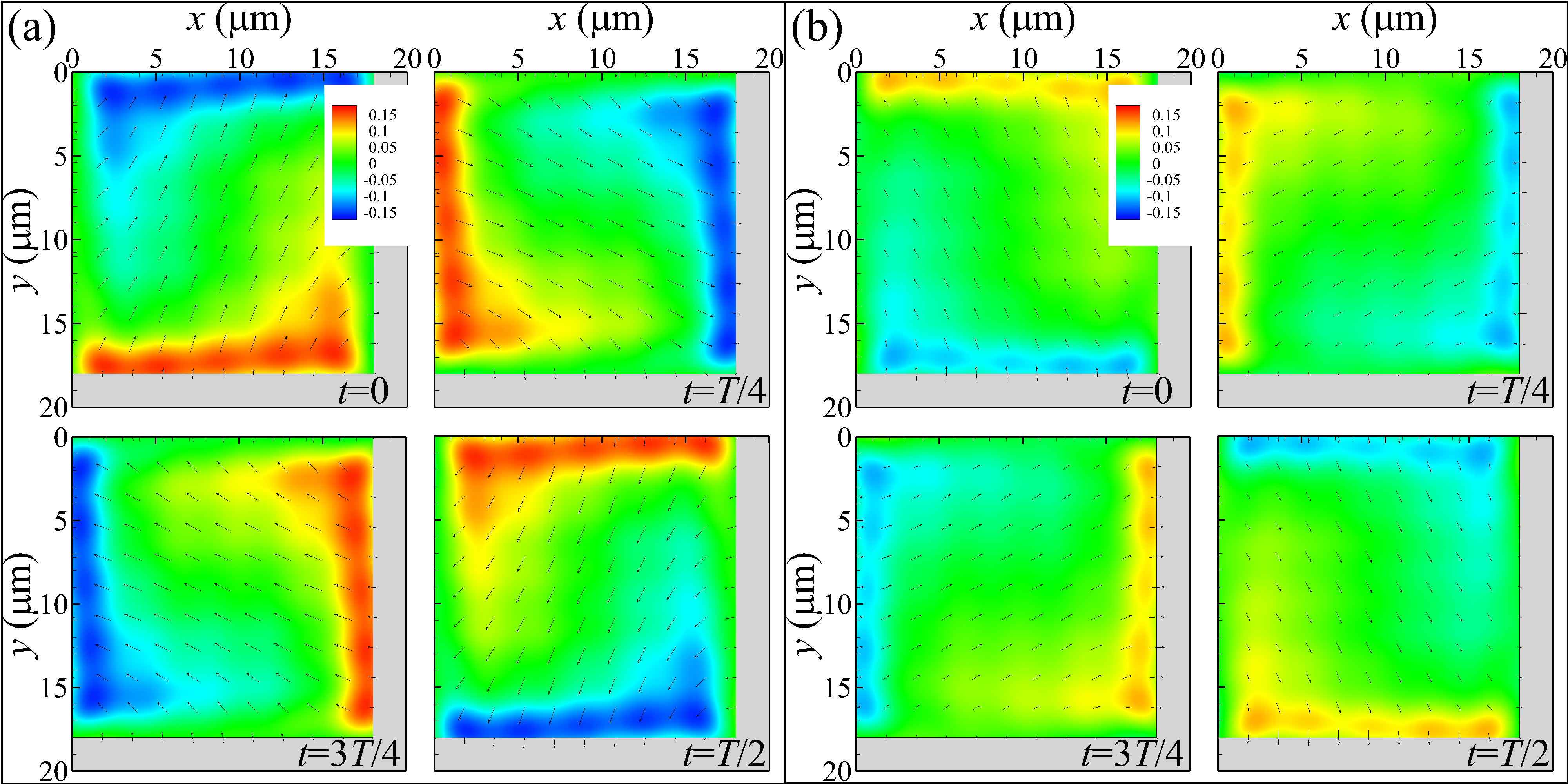
Adding the perforated metal film on top of graphene changes considerably the extinction spectrum. Thus, in the low-frequency region both clockwise and anticlockwise circularly polarized waves [depicted in Figs. 6(c) and 6(d), correspondingly] are characterized by diminished extinction owing to the aforementioned long-wavelength screening. This result is completely different from the extinction spectra of the perforated graphene, considered in Ref. Poumirol et al. (2017): in the low-frequency region perforated graphene exhibits enhanced extinction. Along with this, the extinction values for electromagnetic waves of both polarizations reach their maxima in the vicinity of the magnetoplasmon resonance frequency [which frequencies are calculated from Eq. (156) and depicted in Figs. 6(c) and 6(d) by vertical dash-and-dotted lines]. For the clockwise polarization [Fig. 6(c)] such a behaviour is quite different from that of bare graphene [where the extinction is a monotonically decreasing function of frequency, see Fig. 6(a)]. It is worth noting that in the case of clockwise polarization the graphene with perforated metal film is characterized by the magnetoplasmon-enhanced extinction. Indeed, in the vicinity of magnetoplasmon resonance frequency the extinction of such structure exceeds that of the graphene without metal film. For the anticlockwise polarization [Fig. 6(d)] the resonant excitation of magnetoplasmons results in the blue-shift of the extinction maximum, compared to the case of bare graphene [Fig. 6(b)]. Noteworthy, in the low-frequency range the anticlockwise polarized wave is characterized by a negative extinction, which becomes more pronounced at high magnetic field [compare red and blue lines in Fig. 6(d), which correspond to T and T, respectively].
At the same time, for both polarizations high magnetic field provides better correspondence between the frequency of maximal extinction and the frequency of the magnetoplasmon resonance. It can be seen from the comparison of black, red, green and blue solid lines maxima in Figs. 6(c) and 6(d) with the positions of the vertical dash-and-dotted lines of respective colors. Indeed, for T (blue solid and dash-and-dotted line) the difference is neglible. The respective spatial distributions of the electric field on graphene in the vicinity of the magnetoplasmon resonance frequency are shown in Fig. 7 for clockwise and anticlockwise circularly polarized incident waves [Figs. 7(a) and 7(b), respectively]. For both polarizations, component of the electric field (depicted by color map) has a maximum and a minimum near the opposite edges of the square hole at the magnetoplasmon resonance. In other words, the distribution of charge carriers in graphene is dipolar. During one period of the electromagnetic wave, , the dipolar distribution rotates along the hole perimeter in the same direction as the incident wave’s polarization vector, clockwise [Fig. 7(a)] or anticlockwise [Fig. 7(b)].
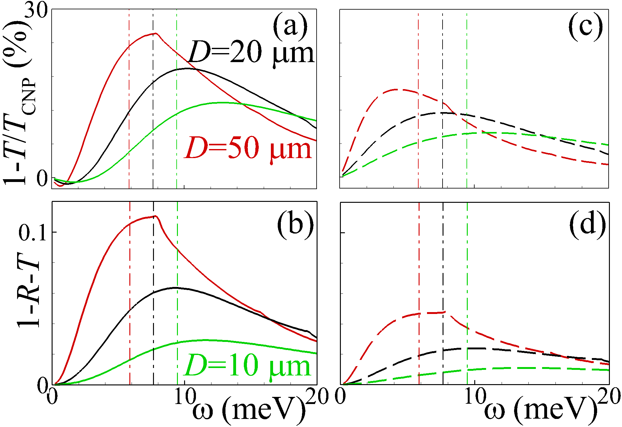
When the graphene is doped with electrons (positive chemical potential, , Fig. 8), the extinction of the clockwise polarized wave [Fig. 8(a)] at high-frequency range is larger than that of the anticlockwise-polarized wave [Fig. 8(c)]. The situation is totally opposite to the case of graphene doped with holes [compare Figs. 8(a) and 6(c) as well as Figs. 8(c) and 6(d)]. Moreover, if compared to the case of the linearly polarized incident wave with the same parameters [shown in Fig. 3], the one with clockwise circular polarization both exhibit a stronger extinction [compare Figs. 8(a) and 3(a)] and stronger absorbance [compare Figs. 8(b) and 3(b)]. At the same time, the case of anticlockwise circular polarization is quite different: here the extinction and the absorbance are considerably lower than those of linearly polarized incident wave [compare Figs. 8(c) and 3(a) as well as Figs. 8(d) and 3(b)]. The dependence of the magnetic circular dichoism upon the parameters of the perforated metal film is described in Appendix C.
V Conclusions
To conclude, we calculated the spectral dependence of the Faraday rotation and MCD of an electromagnetic wave transmitted through a graphene layer subjected to an external perpendicular magnetic field. The calculations show that these effects are strongly influenced by adding a periodically perforated metallic film (a 2D grating) on top of graphene. We have demonstrated that, if the width of the perforation holes is close to the array period (i.e. the grating looks like a thin metallic net), the incident electromagnetic wave is strongly screened by this structure in the low-frequency range. It results in a decrease of the Faraday rotation angle of the transmitted wave, in comparison with bare graphene. In contrast, if the wave frequency is close to that of the magnetoplasmon resonance supported by the structure with 2D grating, one can expect an increase of the Faraday rotation angle, which is a result of the magnetoplasmon-mediated transmission. The maximum of the Faraday rotation angle is shifted to higher frequency when the period of the grating decreases. An important advantage of the graphene-based structure with 2D grating is that it introduces lower ellipticity to the transmitted linear-polarized wave and for some frequencies it can vanish, which means maintaining the linear polarization (see Fig. 3). It can be potentially interesting for making a switchable rotating polariser in the THz range by combining a stack of graphene layers with a thin metal net on top of each of them in order to get high rotation angles.
The effect introduced by the grating is even more substantial for the MCD, which is quantified by the difference in the extinction between left-hand and right-hand circular polarized waves444Alternatively, it can be quantified in terms of the coefficient of circular dichroism introduced in Appendix C. (Fig. 8). We notice that the dichroism changes its sign depending on the wave frequency and the crossover point in the spectrum can be tuned by adjusting magnetic field and also the graphene Fermi energy that determine the magnetoplasmon dispersion curve. This opens the way to design an electrically switchable optical isolator based on the MCD effect by utilizing non-reciprocal losses.Poumirol et al. (2017)
One possible extension of this work can be the study of other (non-square) types of hole arrays (e.g. triangular, rectangular, etc.), which are nonsymmetric with respect to the polarization plane of the incident wave. In this case the transmittance and the Faraday rotation angle will depend upon the direction of polarization of the incident wave with respect to the translation vectors of the 2D grating. Another possible further development of the present work may consist in taking into account the dependence of the substrate dielectric constant upon the magnetic field, which can result in the additional anisotropy and, as a consequence, in a dependence of the transmittance upon the direction of the external magnetic field. It can also be interesting to consider a thin spacer between the graphene and the metal grating that could work as a resonator and can eventually enhance the magnetoplasmon’s amplitude and the effect induced by them in the structure. Also this type of structure allows one to use graphene magnetoplasmons for the controlling of spoof plasmons in the metal grating Dias and Peres (2017) as well as the enhanced optical transmission Ebbesen et al. (1998).
Acknowledgements.
The authors thank Alexey Kuzmenko from the University of Geneva, Switzerland and Luis Martín-Moreno from the University of Zaragoza, Spain for the careful reading, valuable discussions and comments. Funding from the European Commission within the project ”Graphene-Driven Revolutions in ICT and Beyond” (ref. no. 696656) and the Portuguese Foundation for Science and Technology (FCT) in the framework of the Strategic Funding UID/FIS/04650/ 2013 is gratefully acknowledged.Appendix A Explicit form of the electromagnetic fields
Assuming electromagnetic field time-dependence as , we represent the Maxwell equations as
| (158) | |||
| (159) | |||
| (160) | |||
| (161) |
where is the frequency, is the velocity of light in vacuum. The superscripts correspond to the spatial domains , , and , respectively. Consequently, the dielectric constants are: , . After substituting Eq. (158) into (159), and using Eq. (160), one obtains:
| (162) |
In a similar manner, substitution of Eq. (159) into (158) gives [taking into account Eq. (161)]:
| (163) |
Incide the holes in the metal film (spatial domain , ), we can consider components of the electromagnetic field, and , as independent variables, thus
| (164) | |||
| (165) |
As a result, we can divide eigenfunctions into two types: (i) E-waves with , and (ii) H-waves with , . For E-waves after matching boundary conditions at the hole edges inside the film , , we obtain the solution of Eq.(164) for the electric field’s component inside the film in the form
where are the mode indices; and are the amplitudes of the respective mode (sin- and cos-like wave, correspondingly), . Other components of the E-wave electromagnetic field can be represented as
Notice that Eqs. (A)–(A) also satisfy other natural boundary conditions: zero tangential component of the electric field and zero normal component of the magnetic field at hole surfaces, , , , .
For H-wave the solution of Eq. (165) for the component of the magnetic field can be represented as
while other components of electromagnetic field are
Here and are the amplitudes of sin- and cos-like waves. It should be emphasized that in the case of H-wave along with modes with nonzero indexes , the existence of modes with one zero and another nonzero index (like , or , ) is possible. Notice that Eqs. (A)–(A) also satisfy the above-mentioned boundary conditions at hole walls , , , . At the same time, there is no mode with (in the summation in Eq. (A) this term is implicitly excluded), because in this case it is impossible to satisfy above-mentioned boundary conditions on hole walls. Using Eqs. (A), (A), (A), (A), it is possible to obtain Eq. (36), which represent the and components of the total magnetic field , in the matrix form. Similarly, Eq. (44) for the and components of the total electric field , , written in the matrix form, can be obtained from Eqs.(A), (A), (A), (A).
Both inside the semi-infinite air (, ) and the semi-infinite substrate (, ) we choose transverse ( and ) components of the magnetic field , as independent variables, thus
| (176) | |||
| (177) |
Also we represent solutions of wave equations (176) and (177) as two-dimensional Fourier series with respect to the harmonics with wavevector in plane . As a matter of fact, electromagnetic field in vacuum can be represented as
| (183) | |||||
At the same time, the electromagnetic field components in the substrate are:
| (189) | |||||
Equations (A), (A), (A), and (A) can be written in the matrix form [see Eq. (II)], while Eqs. (A), (A), (A), and (A) can be transformed into Eq. (II).
In order to calculate the reflectance and transmittance we notice that the flux density of energy is decribed by the Poynting vector . Respectively, using Eqs. (A) and (A), the component of the Poynting vector of the -harmonics in the substrate can be represented as
In the matrix form this relation can be represented as
| (193) | |||
| (194) | |||
| (199) |
In the air, the component of the Poynting vector of the reflected wave’s -harmonic [using Eqs. (A) and (A)] is written as
| (205) |
The difference of sign in Eqs. (A) and (A) reflects the fact that the energy flux of the transmitted wave [see Eq. (A)] flows in the positive direction of axis, while that of reflected wave [see Eq. (A)] flows in the negative direction of axis. Using the same formalism for the incident wave, we obtain the component of its Poynting vector in the form:
| (206) |
Appendix B Transmittance of the graphene layer without periodical structure and the dispersion relation of magnetoplasmons
When the metal film is absent (), then right-hand sides of Eqs. (52) and (90) become equal [as well as those of Eqs. (69) and (105)]. As a consequence, the equality of left-hand sides of Eqs. (52) and (90) gives
| (213) | |||
| (216) | |||
| (219) | |||
| (222) | |||
| (225) |
As in Sec. II, we multiply Eqs. (216) and (225) by and integrate over the area of one period of the structure , . We obtain:
| (230) | |||
| (233) | |||
| (238) | |||
| (241) |
B.1 Dispersion relation of magnetoplasmons
When or , Eqs. (233) and (241) take the form
| (246) | |||
| (251) |
As a result, the amplidues of the magnetic field components corresponding to the transmitted wave are governed by the equation
| (254) | |||
| (255) |
with
being the inverse of the matrix . If we project , on the direction of the wavevector , we have
where
is the transformation matrix, and are the components of the magnetic field in the substrate, parallel and perpendicular to the harmonic wavevector . In this case Eq. (255) can be rewritten as
| (261) |
and the matrix
after some algebra will have the form
Here we took into account that , . The Eq. (261) possesses a solution, only when the determinant of matrix is equal to zero. Thus, the magnetoplasmon dispersion relation is
which after the formal substitution can be transformed into Eq. (156).
B.2 The transmittance and the reflectance of the graphene layer on substrate
When , Eqs. (233) and (241) have the form
| (269) | |||
| (270) | |||
| (277) | |||
| (278) |
Taking into account that , , matrixes can be represented in the simple form,
| (279) |
and Eqs. (270) and (278) can be rewritten as
| (286) | |||
| (287) | |||
| (294) | |||
| (295) |
Multiplying Eq. (295) by and summing with Eq. (287) we obtain:
| (300) |
where the matrix
and we took into account that , . As a result, the solution of Eq. (300) can be represented as
| (302) | |||
| (303) |
Similarly, combining Eqs. (300) and (295), one can obtain the expression for the amplitude of the reflected wave magnetic field:
or, equivalently
Taking into account the particular form of the matrices and [see Eq. (279)], the expressions (194) and (A) for transmitted and reflected wave energy flux density in direction are written as
Accordingly, from Eqs. (207) and (208) the transmittance and reflectance can be expressed as
| (309) | |||
| (310) |
Finally, after substituting the expressions for the magnetic field components, (302)–(LABEL:eq:Hry-00) into Eqs. (309) and (310) one can obtain the transmittance and the reflectance of bare graphene in the following form:
| (311) | |||
| (312) |
Appendix C Coefficient of magnetic circular dichroism
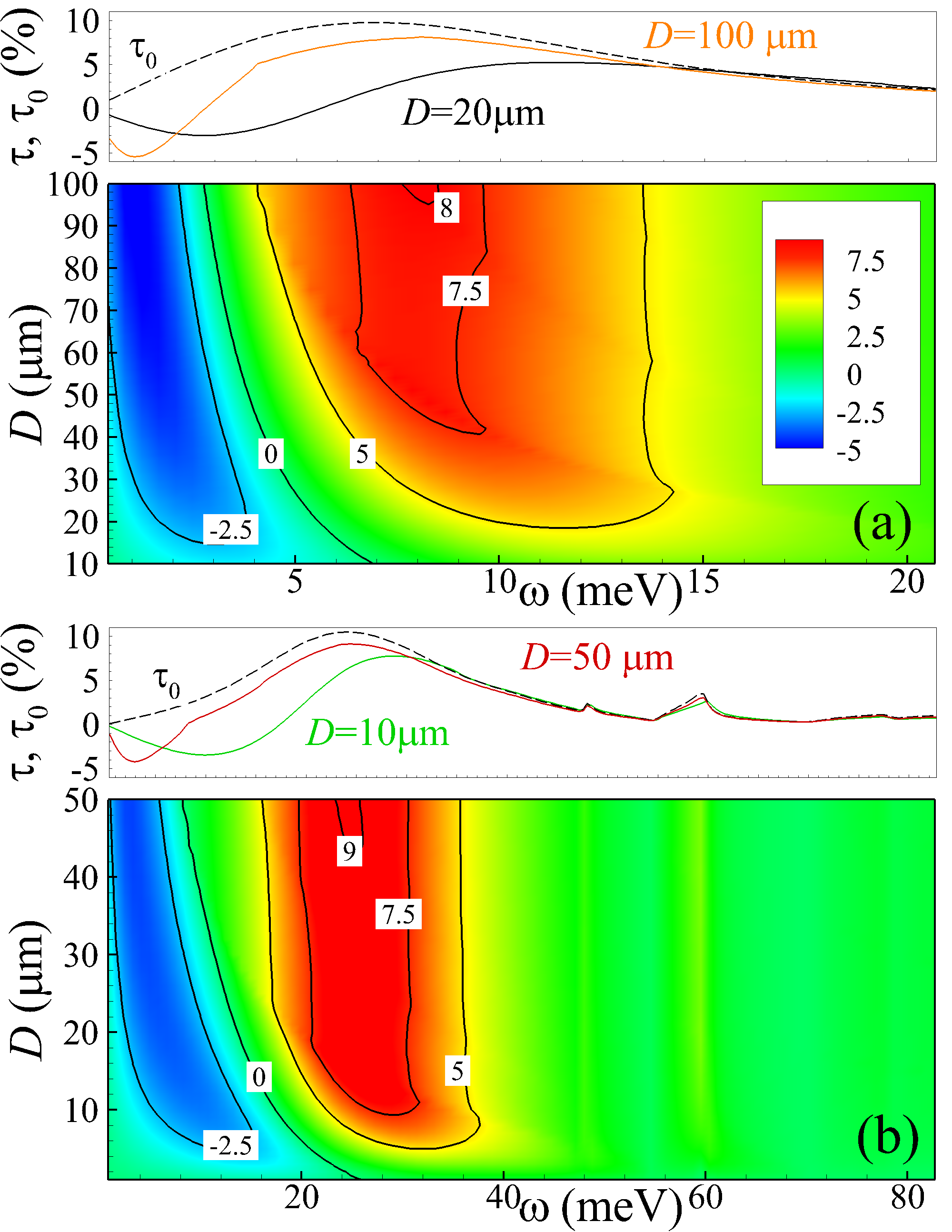
In order to characterize quantitatively the circular dichroism in our magnetoactive graphene-based structure, we introduce the coefficient of circular dichroism,
which is expressed in terms of the transmittance of the clockwise and anticlockwise circularly polarized waves and . The dependence of the coefficient of the circular dichroism upon the frequency and the period of the hole array is shown in Fig. 9. It can be seen that the coefficient of the optical dichroism achieves its maximum in the vicinity of meV [for weak magnetic field, see Fig. 9(a)] or meV [for strong magnetic field, see Fig. 9(b)]. The maximal value of the optical dichoism coefficient grows monotonically with the increase of the hole array period . Notice that the coefficient of optical dichroism of the perforated metal film deposited on top of graphene monolayer is always smaller than that of bare graphene, [compare dashed and solid lines in upper plots in Figs. 9(a) and 9(b)]. In other words, the presence of the perforated metallic film on top of the graphene sheet reduces the relative contrast between the transmittances of clockwise- and anticlockwise-polarized waves. The physical reason for this is the diffraction of the incident electromagnetic wave on the graphene with periodic structure, which gives rise to the partial conversion of the incident wave energy into the energy of the excited magnetoplasmons, thus reducing the transmittance of this structure for both circular polarizations (clockwise and anticlockwise). However, the stronger decrease of the anticlockwise circularly polarized wave transmittance (compared to that of clockwise polarized wave) leads to the reduction of the circular dichroism coefficient .
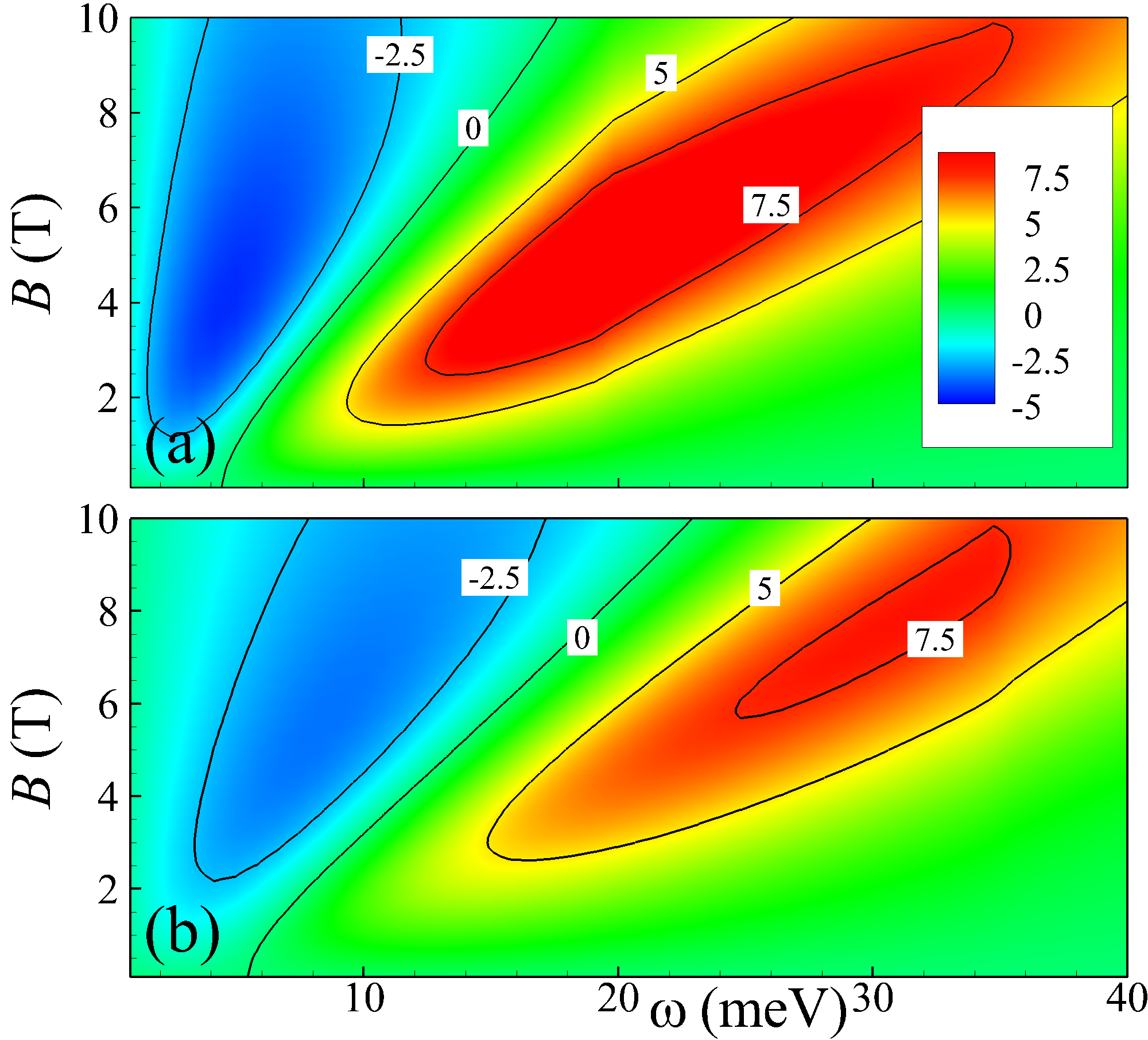
Moreover, the presence of the perforated metal film on top of graphene results into the possibility to obtain a negative circular dichroism coefficient (hence, ) at the low-frequency region. This situation is in strong contrast with the case of bare graphene without perforated metal film on top of it, where the coefficient of circular dichroism is always possitive [, see upper plots in Figs. 9(a) and 9(b)]. It should be stressed that a decrease of the grating period [as shown in Fig. 9] and an increase of the magnetic field [see Fig. 10] lead to a broadening of the frequency region with negative .
References
- Faraday (1846) M. Faraday, Philos. Trans. Roy. Soc. London 136, 1 (1846).
- Gabriel and Brodwin (1965) G. Gabriel and M. Brodwin, IEEE Trans. Microwave Theory Tech. 13, 364 (1965).
- Auracher and Witte (1975) F. Auracher and H. H. Witte, Opt. Commun. 13, 435 (1975).
- Dötsch et al. (2005) H. Dötsch, N. Bahlmann, O. Zhuromskyy, M. Hammer, L. Wilkens, R. Gerhardt, P. Hertel, and A. F. Popkov, Journal of the Optical Society of America B 22, 240 (2005).
- Aplet and Carson (1964) L. J. Aplet and J. W. Carson, Appl. Opt. 3, 544 (1964).
- Jalas et al. (2013) D. Jalas, A. Petrov, M. Eich, W. Freude, S. Fan, Z. Yu, R. Baets, M. Popović, A. Melloni, J. D. Joannopoulos, M. Vanwolleghem, C. R. Doerr, and H. Renner, Nat. Photonics 7, 579 (2013).
- Ribbens (1965) W. B. Ribbens, Appl. Opt. 4, 1037 (1965).
- Takei and Mizumoto (2010) R. Takei and T. Mizumoto, Japanese Journal of Applied Physics 49, 052203 (2010).
- Tien et al. (1974) P. K. Tien, D. P. Schinke, and S. L. Blank, Journal of Applied Physics 45, 3059 (1974).
- Ishida et al. (2016) E. Ishida, K. Miura, Y. Shoji, T. Mizumoto, N. Nishiyama, and S. Arai, Japanese Journal of Applied Physics 55, 088002 (2016).
- Shoji and Mizumoto (2014) Y. Shoji and T. Mizumoto, Sci. Technol. Adv. Mater. 15, 014602 (2014).
- Shoji et al. (2016) Y. Shoji, K. Miura, and T. Mizumoto, J. Opt. 18, 013001 (2016).
- Qiu et al. (2011) W. Qiu, Z. Wang, and M. Soljačić, Opt. Express 19, 22248 (2011).
- Śmigaj et al. (2010) W. Śmigaj, J. Romero-Vivas, B. Gralak, L. Magdenko, B. Dagens, and M. Vanwolleghem, Opt. Lett. 35, 568 (2010).
- Dmitriev and Kawakatsu (2012) V. Dmitriev and M. N. Kawakatsu, Appl. Opt. 51, 5917 (2012).
- Wang and Fan (2005) Z. Wang and S. Fan, Opt. Lett. 30, 1989 (2005).
- Zhang et al. (2013) L. Zhang, D. Yang, K. Chen, T. Li, and S. Xia, Optics and Laser Technology 50, 195 (2013).
- Fan et al. (2011) F. Fan, Z. Guo, J.-J. Bai, X.-H. Wang, and S.-J. Chang, Journal of the Optical Society of America B 28, 697 (2011).
- Wang et al. (2009) Z. Wang, Y. Chong, J. D. Joannopoulos, and M. Soljačić, Nature 461, 772 (2009).
- Fan et al. (2012) F. Fan, S.-J. Chang, C. Niu, Y. Hou, and X.-H. Wang, Opt. Commun. 285, 3763 (2012).
- Chen et al. (2015a) S. Chen, F. Fan, X. Wang, P. Wu, H. Zhang, and S. Chang, Optics Express 23, 1015 (2015a).
- Chen et al. (2015b) S. Chen, F. Fan, X. He, M. Chen, and S. Chang, Appl. Opt. 54, 9177 (2015b).
- Ozbay (2006) E. Ozbay, Science 311, 189 (2006).
- Stockman (2011) M. I. Stockman, Phys. Today 64, 39 (2011).
- Temnov (2012) V. V. Temnov, Nat. Photonics 6, 728 (2012).
- Armelles et al. (2013) G. Armelles, A. Cebollada, A. García-Martín, and M. U. González, Adv. Opt. Mater. 1, 10 (2013).
- Maksymov (2015) I. Maksymov, Nanomaterials 5, 577 (2015).
- Chiu and Quinn (1972) K. W. Chiu and J. J. Quinn, Il Nuovo Cimento B 10, 1 (1972).
- Temnov et al. (2010) V. V. Temnov, G. Armelles, U. Woggon, D. Guzatov, A. Cebollada, A. Garcia-Martin, J.-M. Garcia-Martin, T. Thomay, A. Leitenstorfer, and R. Bratschitsch, Nat. Photonics 4, 107 (2010).
- Fan et al. (2013) F. Fan, S. Chen, W. Lin, Y.-P. Miao, S.-J. Chang, B. Liu, X.-H. Wang, and L. Lin, Appl. Phys. Lett. 103, 161115 (2013).
- Fan et al. (2016) F. Fan, S.-T. Xu, X.-H. Wang, and S.-J. Chang, Opt. Express 24, 26431 (2016).
- Firby and Elezzabi (2015) C. J. Firby and A. Y. Elezzabi, Optica 2, 598 (2015).
- Davoyan and Engheta (2013) A. R. Davoyan and N. Engheta, New J. Phys. 15, 083054 (2013).
- Firby and Elezzabi (2016) C. J. Firby and A. Y. Elezzabi, Opt. Lett. 41, 563 (2016).
- Chin et al. (2013) J. Y. Chin, T. Steinle, T. Wehlus, D. Dregely, T. Weiss, V. I. Belotelov, B. Stritzker, and H. Giessen, Nat. Commun. 4, 1599 (2013).
- Caballero et al. (2015) B. Caballero, A. García-Martín, and J. C. Cuevas, Opt. Express 23, 22238 (2015).
- Belotelov et al. (2011) V. I. Belotelov, I. A. Akimov, M. Pohl, V. A. Kotov, S. Kasture, A. S. Vengurlekar, A. V. Gopal, D. R. Yakovlev, A. K. Zvezdin, and M. Bayer, Nat. Nanotechnol. 6, 370 (2011).
- Kreilkamp et al. (2013) L. E. Kreilkamp, V. I. Belotelov, J. Y. Chin, S. Neutzner, D. Dregely, T. Wehlus, I. A. Akimov, M. Bayer, B. Stritzker, and H. Giessen, Phys. Rev. X 3, 041019 (2013).
- Xiao et al. (2016) S. Xiao, X. Zhu, B.-H. Li, and N. A. Mortensen, Frontiers of Physics 11, 117801 (2016).
- García de Abajo (2014) F. J. García de Abajo, ACS Photonics 1, 135 (2014).
- Chen et al. (2017) P.-Y. Chen, C. Argyropoulos, M. Farhat, and J. S. Gomez-Diaz, Nanophotonics 6, 1239 (2017).
- Bludov et al. (2013) Y. V. Bludov, A. Ferreira, N. M. R. Peres, and M. I. Vasilevskiy, International Journal of Modern Physics B 27, 1341001 (2013).
- Low and Avouris (2014) T. Low and P. Avouris, ACS Nano 8, 1086 (2014), 1403.2799 .
- Koppens et al. (2011) F. H. L. Koppens, D. E. Chang, and F. J. García de Abajo, Nano Lett. 11, 3370 (2011).
- Nikitin et al. (2011) A. Y. Nikitin, F. Guinea, F. J. García-Vidal, and L. Martín-Moreno, Phys. Rev. B 84, 195446 (2011).
- Novoselov et al. (2005) K. S. Novoselov, A. K. Geim, S. V. Morozov, D. Jiang, M. I. Katsnelson, I. V. Grigorieva, S. V. Dubonos, and A. A. Firsov, Nature 438, 197 (2005).
- Zhang et al. (2005) Y. Zhang, Y.-W. Tan, H. L. Stormer, and P. Kim, Nature 438, 201 (2005).
- Tamagnone et al. (2014) M. Tamagnone, A. Fallahi, J. R. Mosig, and J. Perruisseau-Carrier, Nat. Photonics 8, 556 (2014).
- Tamagnone et al. (2016) M. Tamagnone, C. Moldovan, J.-M. Poumirol, A. B. Kuzmenko, A. M. Ionescu, J. R. Mosig, and J. Perruisseau-Carrier, Nat. Commun. 7, 11216 (2016).
- Shimano et al. (2013) R. Shimano, G. Yumoto, J. Y. Yoo, R. Matsunaga, S. Tanabe, H. Hibino, T. Morimoto, and H. Aoki, Nat. Commun. 4, 1841 (2013).
- Crassee et al. (2010) I. Crassee, J. Levallois, A. L. Walter, M. Ostler, A. Bostwick, E. Rotenberg, T. Seyller, D. van der Marel, and A. B. Kuzmenko, Nat. Phys. 7, 48 (2010).
- Sounas et al. (2013) D. L. Sounas, H. S. Skulason, H. V. Nguyen, A. Guermoune, M. Siaj, T. Szkopek, and C. Caloz, Appl. Phys. Lett. 102, 191901 (2013).
- Berman et al. (2008) O. L. Berman, G. Gumbs, and Y. E. Lozovik, Phys. Rev. B 78, 085401 (2008).
- Roldán et al. (2009) R. Roldán, J.-N. Fuchs, and M. O. Goerbig, Phys. Rev. B 80, 085408 (2009).
- Crassee et al. (2012) I. Crassee, M. Orlita, M. Potemski, A. L. Walter, M. Ostler, T. Seyller, I. Gaponenko, J. Chen, and A. B. Kuzmenko, Nano Lett. 12, 2470 (2012).
- Yan et al. (2012) H. Yan, Z. Li, X. Li, W. Zhu, P. Avouris, and F. Xia, Nano Lett. 12, 3766 (2012).
- Tymchenko et al. (2013) M. Tymchenko, A. Y. Nikitin, and L. Martín-Moreno, ACS Nano 7, 9780 (2013).
- Poumirol et al. (2017) J.-M. Poumirol, P. Q. Liu, T. M. Slipchenko, A. Y. Nikitin, L. Martin-Moreno, J. Faist, and A. B. Kuzmenko, Nat. Commun. 8, 14626 (2017).
- Kuzmin et al. (2016) D. A. Kuzmin, I. V. Bychkov, V. G. Shavrov, and V. V. Temnov, Nano Lett. 16, 4391 (2016).
- Fallahi and Perruisseau-Carrier (2012) A. Fallahi and J. Perruisseau-Carrier, Appl. Phys. Lett. 101, 231605 (2012).
- Ferreira et al. (2011) A. Ferreira, Y. V. Bludov, V. Pereira, N. M. R. Peres, and A. H. Castro Neto, Phys. Rev. B 84, 235410 (2011).
-
Note (1)
The substrate dielectric function includes optical phonon
response,
where , meV, meV, meV, meV are phonon frequencies, meV, meV, meV, meV are the phonon dampings, and , , , are the weighting coefficients.(313) - Note (2) The expressions for and as well as the details of derivation can be found in Appendix B.2.
- Born and Wolf (1999) M. Born and E. Wolf, Principles of Optics (7th Ed) (Cambridge University Press, 1999).
- Note (3) Excepting narrow frequency windows at , and , where, nevertheless, an increase of the Faraday rotation angle is negligibly small.
- Basu (1997) P. K. Basu, Theory of Optical Processes in Semiconductors (Clarendon Press, Oxford, 1997).
- Note (4) Alternatively, it can be quantified in terms of the coefficient of circular dichroism introduced in Appendix C.
- Dias and Peres (2017) E. J. C. Dias and N. M. R. Peres, ACS Photonics (2017), 10.1021/acsphotonics.7b00629.
- Ebbesen et al. (1998) T. W. Ebbesen, H. J. Lezec, H. F. Ghaemi, T. Thio, and P. A. Wolff, Nature 391, 667 (1998).