Band Splitting in Bilayer Stanene Electronic Structure scrutinized via first principle DFT Calculations
Abstract
The recent work on stanene as quantum spin Hall insulators made us investigate bilayer stanene using first principle calculations. With an aim of improving and developing new properties, via modulating the stacking order (and angle) of the bilayers. This stacking of layers has been proven technique for modulating the properties of monolayer materials. Here we design multiple bilayer systems, with different stacking angles and AA and AB configurations. Rather observing an improvement in bandgap due to spin-orbit coupling (SOC), we witness a splitting of the band due to SOC, a characteristic behavior of stacked MoS2 sheets. This splitting of the bands gives rise to different, independent and distinct spin-up and spin-down channels, manifesting a valley dependent spin polarization. Also, as a contrast to stacked MoS2 system we notice in our system the stacking angle and order, does effect electronic states.
I Introduction
The exfoliation of graphene Graphene has generated a huge interest in the field of condensed matter physics. The honeycomb lattice structure of graphene exhibits necessary features required by the Haldane model Haldane_Model . Materials represented by Haldane model generally host quantum Hall effect. The spin-orbital coupling (SOC) in such materials could lead to quantum spin Hall effect (QSH) Topological_Insulator_Hassan . The first experimental observation of QSH in HgTe quantum well HgTe_Quantum_Well led to the development of topological insulators (TI) Topological_Insulator_Hassan . TIs are the class of material which could assist to bring the dream of creating dissipationless conduction channel for electrons a reality. Two-dimensional versions of these TIs are called as quantum spin Hall insulators (QSHI) 100_Conducting . However, some of the 2D QSHI have a weak SOC, a very small bandgap ( meV), making it unsuitable for most of the applications Graphene_Spin_Hall . Much of the work in the last decade has been dedicated to identification and synthesis of these materials.
One way around is to investigate other honeycomb lattices such as those formed out of group IVA elements right below Carbon in the periodic table. This has led to buckled honeycomb lattice of Silicon and Germanium, which have been computationally verified 2D_Si_Ge_Computational ; 2D_Si_Ge_Computational_2 and experimentally synthesized 2D_Si_Exprimental ; 2D_Ge_Exprimental . Unfortunately, these also have a very small bandgapSi_Ge_band_gap ; 2D_Si_Ge_Computational . A 2D buckled honeycomb lattice of Tin (stanene), which is computationally predicted Tin_Spin_Hall ; Tin_Spin_Hall_2 as a QSHI, is supposed to have a sufficient bandgap required for practical use as QSHI. It was fabricated on Bi2Te3 substrate via molecular beam epitaxy Stanene_Synthesis_China ; Stanene_Synthesis_India . The issue with this is that although it has been synthesized, its electronic states are pinned on the substrates stanene’s valance bands with conduction bands of the substrate, giving stanene a metallic interface and losing its QSHI nature. This unwanted pinning of conducting states have been recently overcome by synthesizing stanene on PbTe substrate, allowing the stanene to retain the bandgapStanene_Synthesis_China_2 . Apart form this recently synthesis of planar stanene has been reported on Ag2Sn substrate Stanene_Synthesis_non_buckled . The bandgap of free-standing stanene is deemed to be sufficient but still small. To improve the bandgap, functionalization as well as passivation with different groups like -H (hydrogenation) Stanene_H , -F (halogen) Tin_Spin_Hall ; Tin_Spin_Hall_2 , -CN (Cyanide) Stanene_CN etc. have been proposed. Studies of van der Waal type structures like stanene on graphene Stanene_on_graphene , stanene between two Ba layer Stanene_between_Ba , have been reported improve the bandgap. Apart from its use as QSHI, stanene also has been predicted to be a very good material to adsorb CO, NOX, SO2, etc. gases Stanene_As_Gas_Absorber . Also, recently stanene’s mechanical property Stanene_mechanical and it applicability in devices Stanene_device have been studied, implying its importance. It may be noted that most of the above-mentioned work is in silico.
In this paper, we perform the first-principle calculations of the bilayer of 2D tin (stanene), stacked similarly to that of the bilayer graphene. A similar approach had been used by Kan et al., for performing density functional theory (DFT) studies on the two lattice of stanene, which are stacked upon each other like AB or Bernal-stacked form. In their study, the bilayer structure had lost its buckling. However, it has been reported that this structure has a lower energy than free-standing stanene making it more stable and having a higher bandgap Bilayer_Stanene . We use a similar approach to construct the stanene bilayer keeping the structure and mechanical exfoliation of bilayer graphene as our template. In addition to varying interlayer spacing, we also varied the stacking angles as discussed in section II. Interestingly, instead of exhibiting a QSHI nature, the proposed systems displayed distinctive attributes of band structure due to band splitting are observed.
II Method
First principle plane waves pseudopotential calculations were performed using the DFT method as implemented in Quantum ESPRESSO (QE) package QE . We have used Perdew-Burke-Ernzerhof (PBE) PBE exchange-correlation functional and included the DFT-D2 van der Waals corrections DFT-D_1 ; DFT-D_2 for representing the electron dispersion effect due to the bilayer. The kinetic energy cutoff was converged at 50 Ry, with a k-point mesh (Monkhorst-Pack) of . To minimize the interaction between neighboring layers, a vacuum Å was set above and below the bilayer. To include the effect of SOC we used fully relativistic pseudopotentials obtained from QE pseudopotential repository website QE_Psudo . The calculation of the band structure and the partial charge densities were performed both with and without SOC Hybrid_no_use . The k-point path for band structure calculations was set according to high symmetry path in Brillouin zone for hexagonal lattices, as . The required k-points for this path were generated using the XCrysDens Xcrystal package.
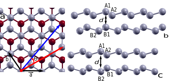
A bilayer structure can be constructed by three types of rotations of one of its layer with respect to the second one: (1) relative rotation between two layers within a single unit cell, (2) rotation one of the entire layer with respect to a reference axis and (3) combination of these two cases. The 2nd and 3rd methods of rotation have been widely used for modification of electronic states in bilayer graphene, boron-nitrate-graphene heterostructures etc. Here a sheet of single layer composed of large number of unit cells is rotated with respect to the second layer. This generates a large number of atoms and electrons in the system. Such a system is extremely difficult to study using the DFT method used in the present work. Generally, tight binding method is preferred for these systems. Further, one of the reasons for the modification of electronic states by interlayer rotation is to break the PT-symmetry, which we could observe with the 1st type rotation for the systems under consideration. Hence, we have carried out the construction of the bilayer stanene using only with the first rotation method.
The construction of the bilayer structures were performed by stacking the two layers of stanene on each other with an interlayer angle as illustrated in figure 1(a). We then changed the angle of top layer with respect to the bottom layer from to in steps of 5∘. However, since these transformations were performed on single unit cell, only 0∘, 5∘, 60∘ and 70∘ angles bilayers could be constructed. For other stacking angles, the resultant structures were found to be discontinuous and/or significantly distorted (see figure SI:1). Therefore, only the un-distorted structures were selected for further analyzes. We label these structures as: S0, S5, S60 and S70, respectively. This process was carried out both configurations of the tin bilayer as described in section III. Next, we varied the interlayer spacing () and computed the total energy as a function of . The structure with lowest energy was selected for the further calculations. Choice of this approach over the conventional geometry optimization method was preferred due to the reason that a bilayer or more layered structure can be mechanically exfoliated from their free-standing monolayer counterpart. These mechanically exfoliated bilayers can be redesigned by simply rotating the layers with respect to each other. This process gives an extra degree of freedom for development of new materials with unique properties. The structures for present work were created using the VNL-Builder (version 2016.3) VNL .
III Result and Discussion
A free-standing stanene monolayer has a buckled honeycomb lattice with two atoms per primitive unit cell. Each of the tin atoms is sp3 hybridized to all its neighboring atoms. It is also known to exhibit two stable configurations based on the extent of buckling. Rivero_PRB_2014 ; Broek_2Dmat_2014 ; Matusalem_PRB_2014 . The optimized structure has a lattice constant of 4.67 Å with a Sn-Sn bondlength of 2.83 Å and a buckling height of 0.86 Å. The energetically less favored low-buckled structure has been investigated more extensively due to its exotic electronic properties.
For the bilayer, a unit cell of a low-buckled structure having the following parameters was used: Å Bilayer_Stanene and Å. The intralayer Sn-Sn bondlength was same as that of the monolayer. An initial separation between the layers was taken to be 2.4 Å. A interlayer spacing of 2.9 Å is reported for their geometry optimized planner bilayer stanene configuration by Kan et al. However, to obtain various configurations and especially the lowest energy structures, we start with a lower interlayer spacing of 2.4 Å. Bilayer stanene inherently has two different geometry due to buckling. To understand the structures, we have labeled the atoms in the top sheet as A1 and A2, representing the top and bottom atom and, B1 and B2 the atoms in the bottom layer, as shown in figure 1(b). If the atom A1 is on top of atom B1 than the system is labeled as AA configuration and if atom A1 is on top of atom B2 than the system is labeled as AB configuration. The nomenclature of these structures is strictly in the context of this paper.
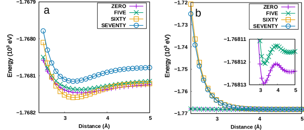
For obtaining the minimum energy structure the interlayer spacing, , was varied in the steps of 0.1 Å, and the total energy was computed for each structure. The plot of energy versus interlayer spacing is given in figure 2. The spacing corresponding to the lowest energy is given in table 1. From table 1 and the figure 2 only one minimum is observed for the AA configuration for all angles of rotation of the top layer with respect to the bottom layer. On the other hand, for the AB configuration, two minima are observed for S0 and S5 structures. For reference check figure 2. Further, to determine if the proposed systems were energetically favorably, their cohesive energies per atom were calculated (see the supplementary information TABLE-I). The cohesive energies of all the bilayer stanene structures studied are of the same order as that of the mono-layer stanene indicating that the proposed systems are energetically stable. We then selected the structures with lowest energy for each of the four stacking angles for further analyzes.
| Configuration | d (Å) | |||
|---|---|---|---|---|
| AA | 3.4 | 3.4 | 3.2 | 3.2 |
| AB | 3.2 (4.7) | 3.3 (4.7) | 4.6 | 4.6 |
The band structures along the high symmetry points () with and without SOC are shown in figure 3 and 4 for configurations AA and AB, respectively. It is clear from the band structures that SOC does not open up a gap (as expected in QSHI) but induces a band splitting. Interestingly, in one of the case, this band splitting decisively converts the semimetallic nature of the system to a metallic one while in other the semiconducting nature is converted into metallic. Such a behavior for materials having Haldane model has not been reported. As the conversation is due to band splitting via SOC, the split in bands could have different up and down states which can be exploited for applications in valleytronics Valleytronics . Hence, only the systems expressing this transition were further investigated, the system with AA configuration having a stacking angle of (AA-S5) and AB configuration having a stacking angle of (AB-S70). In order to understand the nature of band splitting, a cue from the work of Zheng et al. MOS_SOC_SPLITING_1 and Zhu et al. MOS_SOC_SPLITING_2 on bilayer MoS2 is taken as the template. The calculated results along with band decomposed charge density at specific k-points were investigated by the same method employed by Zheng et al. MOS_SOC_SPLITING_1 and Zhu et al. MOS_SOC_SPLITING_2 due to the similarity of their and our systems in terms of geometric and electronic structure.
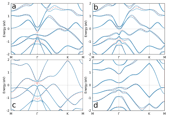
The figure 5 is an enlarged version of the band structure of AA-S5 having an interlayer spacing of 3.38 Å. From the non-SOC band structure represented in red dotted lines, a semimetallic nature is observed due to the interaction between band at point and the band left to point. Also, an indirect bandgap is observed between the band next to point and the band at point. When the SOC interaction is taken into consideration, the former set of the bands overlap, while the latter indirect bandgap is closed. Let the band at point be labeled as “G” before splitting and as “G1” “G2” for the top and bottom bands, respectively, after splitting due to SOC. Similarly, the bands corresponding to the point be labeled as “K”, “K1” and “K2” and the bands toward the left side of the point are labeled as “LK”, “LK1” and “LK2”, respectively. The energy difference between the bands LK1 and LK2 is LK=95 meV and that between K1 and K2 is K=74 meV. Clearly, the above effect is due to inclusion of SOC.
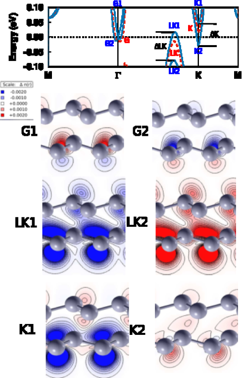
We also plot the band decomposed charge density for those k-points as their characteristic is well documented and have been used for the similar analyzes MOS_SOC_SPLITING_1 ; MOS_SOC_SPLITING_2 . By including the magnetization direction (of bands) and observations from band decomposed charge density, we note the following: G1 has state, G2 has state, K1 has state, K2 has state, LK1 has state and LK2 has state. Thus, in the direction from to point the down channels overlap while the up channel has an indirect bandgap of meV. It may also be noted that system only provides a conducting up (down) channel and an indirect bandgap for the up (down) channel of the magnitude of 28.13 (49.29) meV, in the direction of and points. We can thus conclude that there are distinct up and down channels. Further, the splitting at point may seem to be Rashba-type splitting as the system has all the necessary requirements such as lack of inversion symmetry, band splitting due to SOC and band splitting at point Rashba_split . However, a charge density analysis show that it is not. Interestingly, the characteristics of band structure is dominated by the bands at and near point.
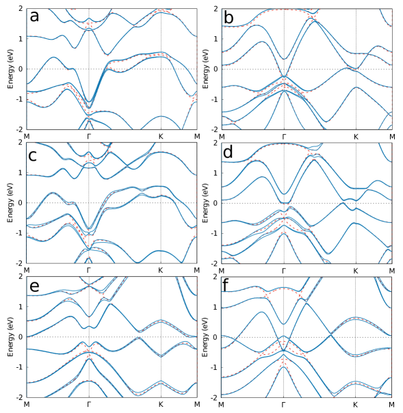
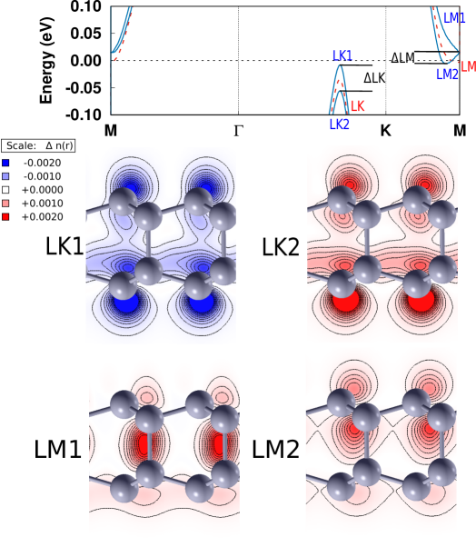
The above-mentioned methodology can be used to interpret the band structure of the AB-S70 having an interlayer spacing =4.60 Å. From the band structure in figure 6, an indirect bandgap between the band left to the point and band left to point of the magnitude of 31 meV. Due to the SOC, an indirect bandgap is reduced to null, while converting the semiconducting nature of the material into semimetallic due to the splitting in both bands. Using the same labeling convention as described earlier, the band left to point is labeled as “LK” - before splitting, “LK1” and “LK2” - after splitting with an energy difference between them being LK=48 meV. Similarly, the band left to the point is labeled as “LM”, “LM1” and “LM2”. having an energy difference between LM1 and LM2 band is LM=22 meV. From the band decomposed charge density (figure 6), along with the direction of magnetization of band we get, LK1 as state, LK2 as state and LM1 as state, LM2 as state. This again leads to the AB-S70 structure having a distinct channel for up state with an indirect gap as 8.41 meV. Hence, from the above observations for both structures, we can assert that the system above provides us with a distinct up channel while the AA-S5 provides up as well as down channel. Such a feature of band splitting has been observed in multilayer MoS2 structure MOS_SOC_SPLITING_2 and is exploited for designing next generation of electronic devices leading to the development of valleytronics Valleytronics , where the energy of an electron and simultaneously valley of the bands is used.
From charge density distribution of bands (Figure 5 and 6) a spread between layers is observed. This spread of charge density can be directly related strength of the interlayer coupling. As the charge density of these bilayer systems is well distributed in between both layers, the interlayer coupling can be considered strong. Additionally, to support that our system has a potential of being used in a valley device, the same procedure was used at the point (other valley). For band structure and band decomposed charge density for the valley, see supporting information (SI:2, SI:3). The calculated results are in an accord that our proposed system do have a merit of being used for valley device.
IV Conclusion
We have studied the bilayer stanene with two stacking configurations AA and AB, using first principle density functional theory. By changing the interlayer spacing and stacking angles we found the minimum energy configuration of the bilayer. For AB stacking configurations of angle 00 and 50, we observed two minima, while the other configurations energies were found to be of the same magnitude. Hence, these systems do have a similar probability of being observed experimentally. Nevertheless, we observe that a change in the stacking angle can affect the electronic properties of the system significantly. Further, by including spin-orbital coupling effects, we observe band splitting, which converts semimetallic nature of the material into metallic. A detailed analyzes of the band structure in conjunction with the band decomposed charge density as well as magnetization directions of bands, we conclude that while the system AB-S70provides a distinct up channel the AA-S5 system provides up as well as down channel, with indirect band gaps. Our work indicates that the mechanically exfoliated bilayer stanene can be used for development of spin and valley physics which can be used for next generation of electronic devices.
V Acknowledgment
The computational work described here is performed at the High Performance Computational Facility at IUAC, New Delhi, India. We would like to express our gratitude to them. Also, we would like to thank the University Grant Commission of India for providing partial funding for the research work through the UGC-BSR Research Startup Grant (Ref. No.F.30-309/2016(BSR)).
References
- [1] Kostya S Novoselov, Andre K Geim, Sergei V Morozov, D Jiang, Y_ Zhang, Sergey V Dubonos, Irina V Grigorieva, and Alexandr A Firsov. Electric field effect in atomically thin carbon films. Science, 306(5696):666–669, 2004.
- [2] F Duncan M Haldane. Model for a quantum hall effect without landau levels: Condensed-matter realization of the” parity anomaly”. Phys. Rev. Lett., 61(18):2015, 1988.
- [3] MZ Hasan and CL Kane. Topological insulators. arXiv preprint arXiv:1002.3895, 2010.
- [4] Markus König, Steffen Wiedmann, Christoph Brüne, Andreas Roth, Hartmut Buhmann, Laurens W Molenkamp, Xiao-Liang Qi, and Shou-Cheng Zhang. Quantum spin hall insulator state in hgte quantum wells. Science, 318(5851):766–770, 2007.
- [5] Will 2-d tin be the next super material? http://phys.org/news/2013-11-d-tin-super-material.html, 2014.
- [6] Charles L Kane and Eugene J Mele. Quantum spin hall effect in graphene. Phys. Rev. Lett., 95(22):226801, 2005.
- [7] S. Cahangirov, M. Topsakal, E. Aktürk, H. Şahin, and S. Ciraci. Two- and one-dimensional honeycomb structures of silicon and germanium. Phys. Rev. Lett., 102:236804, Jun 2009.
- [8] Kyozaburo Takeda and Kenji Shiraishi. Theoretical possibility of stage corrugation in si and ge analogs of graphite. Phys. Rev. B, 50:14916–14922, Nov 1994.
- [9] Boubekeur Lalmi, Hamid Oughaddou, Hanna Enriquez, Abdelkader Kara, Sébastien Vizzini, Bénidicte Ealet, and Bernard Aufray. Epitaxial growth of a silicene sheet. Appl. Phys. Lett., 97(22):223109, 2010.
- [10] ME Dávila, Lede Xian, Seymur Cahangirov, Angel Rubio, and Guy Le Lay. Germanene: a novel two-dimensional germanium allotrope akin to graphene and silicene. N. J. of Phys., 16(9):095002, 2014.
- [11] Yafei Ren, Zhenhua Qiao, and Qian Niu. Topological phases in two-dimensional materials: a review. Reports on Progress in Physics, 79(6):066501, 2016.
- [12] Yong Xu, Binghai Yan, Hai-Jun Zhang, Jing Wang, Gang Xu, Peizhe Tang, Wenhui Duan, and Shou-Cheng Zhang. Large-gap quantum spin hall insulators in tin films. Phys. Rev. Lett., 111(13):136804, 2013.
- [13] Cheng-Cheng Liu, Hua Jiang, and Yugui Yao. Low-energy effective hamiltonian involving spin-orbit coupling in silicene and two-dimensional germanium and tin. Physical Review B, 84(19):195430, 2011.
- [14] Feng-feng Zhu, Wei-jiong Chen, Yong Xu, Chun-lei Gao, Dan-dan Guan, Can-hua Liu, Dong Qian, Shou-Cheng Zhang, and Jin-feng Jia. Epitaxial growth of two-dimensional stanene. Nature materials, 14(10):1020–1025, 2015.
- [15] Sumit Saxena, Raghvendra Pratap Choudhary, and Shobha Shukla. Stanene: Atomically thick free-standing layer of 2d hexagonal tin. arXiv preprint arXiv:1505.05062, 2015.
- [16] Yunyi Zang, Tian Jiang, Yan Gong, Zhaoyong Guan, Menghan Liao, Zhe Li, Lili Wang, Wei Li, Canli Song, Ding Zhang, et al. Realizing an epitaxial stanene with an insulating bandgap. arXiv preprint arXiv:1711.07035, 2017.
- [17] Junji Yuhara, Yuya Fujii, Kazuki Nishino, Naoki Isobe, Masashi Nakatake, Lede Xian, Angel Rubio, and Guy Le Lay. Large area planar stanene epitaxially grown on ag(1?1?1). 2D Materials, 5(2):025002, 2018.
- [18] Sheng-shi Li and Chang-wen Zhang. Tunable electronic structures and magnetic properties in two-dimensional stanene with hydrogenation. Mat. Chem. Phys., 173:246–254, 2016.
- [19] Wei-xiao Ji, Chang-wen Zhang, Meng Ding, Ping Li, Feng Li, Miao-juan Ren, Pei-ji Wang, Shu-jun Hu, and Shi-shen Yan. Stanene cyanide: a novel candidate of quantum spin hall insulator at high temperature. Sci. Rep., 5:18604, 2015.
- [20] Xianping Chen, Ruishen Meng, Junke Jiang, Qiuhua Liang, Qun Yang, Chunjian Tan, Xiang Sun, Shengli Zhang, and Tianling Ren. Electronic structure and optical properties of graphene/stanene heterobilayer. Phys. Chem. Chem. Phys., 18(24):16302–16309, 2016.
- [21] Steve M Young, S Manni, Junping Shao, Paul C Canfield, and Aleksey N Kolmogorov. Basn : A new, wide-gap, strong topological insulator. arXiv preprint arXiv:1607.05234, 2016.
- [22] Lauren Takahashi and Keisuke Takahashi. Low temperature pollutant trapping and dissociation over two-dimensional tin. Phys. Chem. Chem. Phys., 17(33):21394–21396, 2015.
- [23] Avik Mahata and Tanmoy Mukhopadhyay. Probing the chirality-dependent elastic properties and crack propagation behavior of single and bilayer stanene. Physical Chemistry Chemical Physics, 20(35):22768–22782, 2018.
- [24] T Mukhopadhyay, A Mahata, S Adhikari, and M Asle Zaeem. Probing the shear modulus of two-dimensional multiplanar nanostructures and heterostructures. Nanoscale, 10(11):5280–5294, 2018.
- [25] Chengxi Huang, Jian Zhou, Haiping Wu, Kaiming Deng, Puru Jena, and Erjun Kan. Quantum phase transition in germanene and stanene bilayer: From normal metal to topological insulator. J. Phys. Chem. Lett., 7(10):1919–1924, 2016.
- [26] Paolo Giannozzi, Stefano Baroni, Nicola Bonini, Matteo Calandra, Roberto Car, Carlo Cavazzoni, Davide Ceresoli, Guido L Chiarotti, Matteo Cococcioni, Ismaila Dabo, et al. Quantum espresso: a modular and open-source software project for quantum simulations of materials. J. of Phys. Cond. Matt., 21(39):395502, 2009.
- [27] John P. Perdew, Kieron Burke, and Matthias Ernzerhof. Generalized gradient approximation made simple. Phys. Rev. Lett., 77:3865–3868, Oct 1996.
- [28] Vincenzo Barone, Maurizio Casarin, Daniel Forrer, Michele Pavone, Mauro Sambi, and Andrea Vittadini. Role and effective treatment of dispersive forces in materials: Polyethylene and graphite crystals as test cases. Journal of Computational Chemistry, 30(6):934–939, 2009.
- [29] Stefan Grimme. Semiempirical gga-type density functional constructed with a long-range dispersion correction. Journal of Computational Chemistry, 27(15):1787–1799, 2006.
- [30] Quantum espresso psudopotential rseudopotentials repository. http://www.quantum-espresso.org/pseudopotentials/.
- [31] We have not used the hybrid functionals for the present work which is generally used for studying this class of systems. Here, we would like to make the following argument regarding our choice: the transition from the semi-metallic to metallic nature is due to the inclusion of SOC as SOC is inherently strong in Sn and represents the system more accurately. We would like to point out that the SOC in Sn is inherently strong and represents the system very accurately which indicates that the bilayer stanene are indeed metallic in nature. An analogy to this can be found in an earlier work (Phys. Rev. Lett. 106, 018301) where SOC was required to explain the voltage generated by the battery. As the system is metallic, the benefit from the hybrid functionals is not significant enough to justify the computational expenses it requires. Hence, the present level of theory is sufficient to provide reasonably accurate results and understanding of band splitting in the systems under consideration.
- [32] Anton Kokalj. Computer graphics and graphical user interfaces as tools in simulations of matter at the atomic scale. Comp. Mat. Sci., 28(2):155–168, 2003.
- [33] Virtual nanolab version 2016.3, quantumwise a/s. www.quantumwise.com.
- [34] P. Rivero, J. A. Yan, V. M. Garc’ia-Su’arez, J. Ferrer, and S. Barraza-Lopez. Phys. Rev. B, 90:241408(R), 2014.
- [35] B. van den Broek, M. Houssa, E. Scalise, G. Pourtois, and V. V. Afanas ev. 2D Mater, 1:021004, 2014.
- [36] B. van den Broek, M. Houssa, E. Scalise, G. Pourtois, and V. V. Afanas ev. Phys. Rev. B, 92:045436, 2015.
- [37] John R Schaibley, Hongyi Yu, Genevieve Clark, Pasqual Rivera, Jason S Ross, Kyle L Seyler, Wang Yao, and Xiaodong Xu. Valleytronics in 2d materials. Nature Reviews Materials, 1:16055, 2016.
- [38] Xiaofeng Fan, David J Singh, and Weitao Zheng. Valence band splitting on multilayer mos2: Mixing of spin–orbit coupling and interlayer coupling. J. Phys. Chem. Lett., 7(12):2175–2181, 2016.
- [39] Xiaofeng Fan, WT Zheng, Jer-Lai Kuo, David J Singh, CQ Sun, and W Zhu. Modulation of electronic properties from stacking orders and spin-orbit coupling for 3r-type mos2. Sci. Rep., 6:24140, 2016.
- [40] Aurelien Manchon, Hyun Cheol Koo, Junsaku Nitta, SM Frolov, and RA Duine. New perspectives for rashba spin-orbit coupling. arXiv preprint arXiv:1507.02408, 2015.