Transmission and reflection of charge density waves in a quantum Hall edge controlled by a metal gate
Abstract
Quantum energy teleportation (QET) is a proposed protocol related to the quantum vacuum. The edge channels in a quantum Hall system is well suited for the experimental verification of QET. For this purpose, we examine a charge density wave excited and detected by capacitively coupled front gate electrodes. We observe the waveform of the charge density wave, which is proportional to the time derivative of the applied square voltage wave. Further, we study the transmission and reflection behaviors of the charge density wave by applying a voltage to another front gate electrode to control the path of the edge state. We show that the threshold voltages where the dominant direction is switched in either transmission or reflection for dense and sparse waves are different from the threshold voltage where the current stops flowing in an equilibrium state.
The physics of the quantum vacuum and its fluctuations (zero-point fluctuations) have attracted considerable attention in various fields of modern physics vacuum . Quantum energy teleportation (QET) is one quantum-vacuum-related protocol hotta ; hottaJPA . By this protocol, the local zero-point energy is extracted from a remote place by only sending classical information, which does not carry energy but contains how to extract energy from the local vacuum. In order to verify this quantum protocol by experiment, a quantum Hall (QH) system has been theoretically suggested to be the best suited physical system yusa ; hotta2014 . The QH states consist of two regions—bulk and edge. When a strong perpendicular magnetic field is applied to the two-dimensional (2D) electrons, the orbital degree of freedom of the electrons in the bulk region is quantized and does not contribute to the transport. However, electrons in the edge region can flow without backscattering, leading to a zero longitudinal resistance yoshioka . Using intriguing properties of edge channels and the charge density waves propagating along them, pioneering experiments have been performed allen ; ashoori ; feve ; kamata ; hashisaka . To perform the QET protocol, excitation and detection through capacitively coupled gate electrodes are required yusa ; hotta2014 . In most experiments, however, the charge density wave in the edge channel has been measured through ohmic contacts as a current flow kamata ; hashisaka . The study of detection by a capacitively coupled contact is very limited ashoori . In this paper, we establish a detection scheme for measuring the charge density wave through a capacitively coupled gate electrode as a key ingredient for experimental verification of the QET protocol.
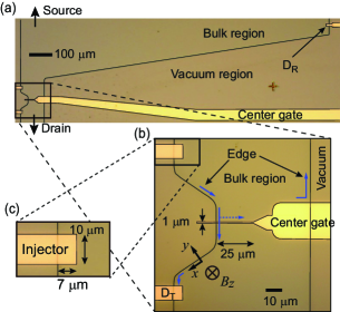
We used a GaAs/AlGaAs single heterostructure as a 2D system. The as-grown electron density and mobility at mK are cm-2 and cm2/(Vs), respectively. Using photolithography and electron-beam lithography, we fabricated the device shown in Fig. 1. The center gate connected to a direct current (dc) voltage source can deplete the electrons under the gate with the application of a negative center gate voltage . Thus, a change in can alter the path of the edge channel from the injector to either of the two detectors, D or D. We define transmission as the path along which a charge density wave is transmitted through the center gate and reflection as the path along which a charge density wave is reflected by the center gate. The injector, D, and D are front gate electrodes made with - and -nm-thick Ti and Au. They are capacitively coupled with the edge channels in an equivalent manner. Moreover, electron-beam lithography was used to process them and the narrow region of the center gate. A voltage signal from a function generator is transmitted to the injector to excite a charge density wave, which propagates along the edge channel in the directions indicated by blue arrows in Fig. 1(b). D and D are connected to an oscilloscope at room temperature through a coaxial cable. The voltage signals measured by the -MHz bandwidth oscilloscope from D and D are and , respectively. No filters or amplifiers are introduced between the detectors and the oscilloscope. The experiment was performed with a magnetic field T applied along the axis perpendicular to the 2D plane. In this condition, the Landau-level filling factor is unity. The typical base temperature is mK.
First, we tested the behavior of the center gate. We applied an alternating voltage with an amplitude mV oscillating at 13 Hz between the source and the drain, i.e., two ohmic contacts. The current between them, , was measured by the lock-in technique as a function of . By decreasing , decreases at V because the electrons under the center gate are depleted, and the electron flow between the source and the drain is hampered. Below V, becomes , indicating that the bulk regions connected to the source and drain are separated from each other by the depleted region under the center gate.
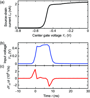
In order to excite a charge density wave, we used a square voltage wave. A typical input voltage was measured by the oscilloscope by direct connection to a signal generator. The typical rise and fall times of the square wave are a few nanoseconds. The waveform has slight under- and overshoots [Fig. 2(b)]. Thus, the time derivative of this square wave has positive and negative peaks corresponding to the rising and falling of the square wave, respectively, and has a small negative peak right after the sharp positive peak at ns in Fig. (c), originating from the overshoot of the square wave. We discuss this waveform of and later in relation to the waveforms observed at D and D.
We injected square waves with amplitudes of V and duration times of ns. With these square waves, a density wave is excited in the edge channel and propagates along the edge, and we measure the waveforms at D and D. We repeatedly performed single-shot measurements times, and the averaged data are displayed in Fig. 3. When is close to V, a voltage signal was only detected at D [Fig. 3(a)], and no signal was detected at D [Fig. (c)]. All waves are transmitted through the center gate because the edge channel is connected from the injector to D but not to D. By decreasing , the amplitude of tends to become weak [Fig. (b)], whereas that of becomes large [Fig. 3(d)], suggesting that some part of the change density wave starts to propagate along the edge formed by the center gate to reach the right-hand side of the sample edge, which is connected to D. In other words, some part of the charge density wave is reflected by the center gate. At V, no signal was detected at D because the center gate is closed and all charge density waves are reflected by the center gate to D.
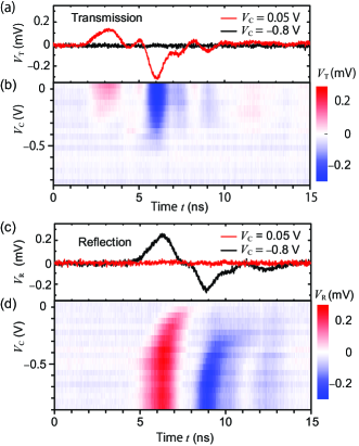
The observed waveforms of and are not analogous to the waveform of the applied voltage [Fig. (b)] but to that of [Fig. (c)]. When a square voltage wave is applied to the injector, the electric field, i.e., the slope of the local confinement potential , becomes small. Since the velocity of the electrons in the edge channel is yoshioka , becomes temporarily small during the rise time of the square pulse, which creates a local dense region in the charge density wave. When the applied voltage becomes constant, i.e., during the flat time region of the square pulse, is also constant over time, and the charge density is constant. Thus, no charge density wave is created. During the fall time, a local sparse region is created because temporarily becomes large. Therefore, the waveform of the charge density wave is proportional to . Note that since the QH state is incompressible, the electron density in the bulk is constant. Thus, the change in the charge density corresponds to the deformation of the edge yoshioka . The dense and sparse regions correspond to the convexity and concavity of the boundary. Since D and D are capacitively coupled to the edge channel, each waveform of and is proportional to the charge density wave.
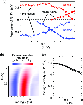
The dependencies of the transmission and reflection of the dense and sparse waves are notable. The peak values of and for dense and sparse waves are plotted as a function of in Fig. 4(a). For the dense wave (red), the transmission and reflection cross each other at V. In contrast, for the sparse wave (blue), it requires a further negative voltage of V for the transmission and reflection to cross each other. Note that the value of at which sharply decreases is V [Fig. 2(a)]. This may be because some electrons can be excited to higher Landau levels when the dense region is created by the rising part of the square wave. In contrast, the electrons in the sparse region cannot be excited because there are no states. In other words, the charge density waves are excited so strongly that the electron–hole symmetry is broken. This is consistent with the fact that the waveforms of the dense and sparse waves observed in reflection [the red line in Fig. 3(c)] are more symmetric with respect to the 0-mV line than those observed in transmission [the black line Fig. 3(a)]. This may be because all of the electrons excited to the higher Landau levels can be easily relaxed by the center gate, which functions as a scattering center, for V, and they do not contribute to the reflection signal. In contrast, for V, the influence of the center gate is small, and the the dense wave is broader than the sparse wave in transmission.
The time difference between the local maximum in at V [Fig. 3(a)] and that in at V [Fig. 3(c)] is ns and is equal to the difference in the arrival times of the charge density waves at D and D. Thus, is , where , , , and are the edge channel length between the center gate to D, that between the center gate to D, that along the center gate, and the velocity of the edge channel along the center gate, respectively. Here, m, mm, and m. Since and the order , can be approximated by , resulting in m/s ( , where is the speed of light).
The local maximum and minimum in appear at and ns, independent of [Fig. 3(b)], whereas those in shift as a function of for V and remain constant for V [Fig. 3(d)]. This may be because the velocity changes when the charge density wave propagates along the center gate electrode, as reported earlier kamata . To obtain systematically, the cross-correlation of at V and at each , i.e., , is calculated as a function of . Here, is the time lag. A strong positive correlation [the red region in Fig. 4(a)] appears near ns, which corresponds to . The average velocity between the center gate and D is plotted as a function of in Fig. 4(c). By decreasing , gradually increases and becomes constant below V.
Acknowledgements.
The authors are grateful for discussions with T. Fujisawa, K. Kobayashi, T. Arakawa, J. N. Moore, R. Schützhold, and W. G. Unruh. This work was supported by the Asahi Glass Foundation; MEXT/JSPS KAKENHI Grant Numbers JP 17H01037 and 16K05311(M.H.); and the “Nanotechnology Support Project” of MEXT.References
- (1) P. W. Milonni, The Quantum Vacuum (Academic Press, 1994).
- (2) M. Hotta, Phys. Lett. A 372, 5671 (2008).
- (3) M. Hotta, J. Phys. A: Math. Theor. 43, 105305 (2010).
- (4) G. Yusa, W. Izumida, and M. Hotta, Phys. Rev. A 84, 032336 (2011).
- (5) M. Hotta, J. Matsumoto, and G. Yusa, Phys. Rev. A 89, 012311 (2014).
- (6) D. Yoshioka, The Quantum Hall Effect (Springer, Berlin, 2002).
- (7) S. J. Allen, H. L. Stormer, and J. C. M. Hwang, Phys. Rev. B 28, 4875 (1983).
- (8) R. C. Ashoori, H. L. Stormer, L. N. Pfeiffer, K. W. Baldwin, and K. West, Phys. Rev. B 45, 3894 (1995).
- (9) G. Fève, A. Mahe, J.-M. Berroir, T. Kontos, B. Plaçais, D. C. Glattli, A. Cavanna, B. Etienne, Y. Jin, Science 316, 1169 (2007).
- (10) H. Kamata, T. Ota, K. Muraki, and T. Fujisawa, Phys. Rev. B 81, 085329 (2010).
- (11) Although we only discuss the average velocity of charge density waves in this paper, one should note that the change of the velocity of the edge channel along the center gate, , appears to be much bigger than reported earlier.
- (12) M. Hashisaka, N. Hiyama, T. Akiho, K. Muraki, and T. Fujisawa, Nat. Phys. doi:10.1038/nphys4062 (2017).