Open Type Nodal line Topological Semimetal in Two Dimensional B2C
Abstract
Topological semimetals, including Dirac semimetals, Weyl semimetals, and nodal line semimetals, receive enormous research interest due to their intrinsic topological nature and fascinating properties. In present work, with the help of density functional theory (DFT), we find that nodal line semimetals and Dirac semimetals can coexist in the low energy electron of two dimensional (2D) monolayer B2C. Intriguingly, besides type-I and type-II Dirac fermions, a kind of open nodal line appears around the Fermi level. The low energy electronic nature of B2C sheet can be described by a tight-binding (TB) model relied on the basis of B-py, pz and C-py, pz states. One of the most merit of the system is that the energy windows of these four types topological semimetals are different that can be easily distinguished in experiments. Moreover, the system provides an excellent platform for studying the interplay between different type semimetals.
Topological semimetal, following the rising of topological insulatorHasan and Kane (2010); Qi and Zhang (2011), has become the hot topic in condensed matter community. Graphene, as the first experimentally synthesized two dimensional (2D) material, is a typical Dirac semimetalWehling et al. (2014) if the weak spin-orbit coupling (SOC) of C atom is neglected. Since the experimental observations of Weyl semimetalsXu et al. (2015); Lu et al. (2015); Lv et al. (2015), more and more researchers turn to these special metal states and explore their possible physical phenomena. Some interesting phenomena, including negative magnetoresistance and non-local transport current, have been predicted in this novel type materialsSon and Spivak (2013); Vazifeh and Franz (2013). Following the discovery of type-II Weyl semimetalSoluyanov et al. (2015), type-II Dirac semimetal was recently proposedHuang et al. (2016); Guo et al. (2017); Chang et al. (arXiv:1606.07555, 2016). Its obvious feature is the violating of the Lorentz symmetry comparing with its type-I counterpart. Nodal line semimetal, whose fermi surface is composed by one or several closed lines, also received considerable attention due to its topological nature. The nodal line semimetal was firstly predicated in three dimensional (3D) materials, including all-carbon Mackay-Terrones crystalWeng et al. (2015), anti-perovskite Cu3PdNYu et al. (2015, 2016), and experimentally observed in 3D materials such as PbTaSe2Bian et al. (2016), PtSn4Wu et al. (2016), and ZrSiSSchoop et al. (2016). Lately, several 2D nodal line semimetals, including Honeycomb-Kagome LatticeLu et al. (arXiv:1603.04596, 2016), 2D MX (M=Pd, Pt; X=S, Se, Te)Jin et al. (arXiv:1608.05791, 2016), bipartite square latticeYang et al. (arXiv:1612.06562, 2016), and topological (crystalline) insulators thin filmNiu et al. (arXiv:1703.05540, 2017), have been proposed theoretically. Besides the compatibility with the synthesis of nano-electronics devices, one of the most significant merits of the 2D topological semimetals is that their topological states can be directly characterized by angle-resolved photoemission spectroscopy (ARPES) in experiments, which provides perfect platform for the investigation of the topological nature.
In present work, with the help of density functional theory (DFT), we find that a novel open type nodal line topological semimetal can coexist with type-I and type-II Dirac semimetal in 2D low buckled B2C. Further investigation also proves that closed type nodal line, open type nodal line, and type-I and type-II Dirac fermions can be found simultaneously in the low energy electronic states of flattened B2C. Moreover, the four types of topological states appear in different energy windows that can be observed and compared in the same experimental observation. With the help of the analysis of the edge states and effective model of the material, the origin of the topological nature was explained. Based on maximally localized Wannier functions, tight-binding model was constructed to investigate the formation of electronic states around Fermi level. Our further particle swarm optimization calculations prove that 2D B2C is feasibly synthesized on the surface of Cu(110) or Ni(110) in experiments, which is crucial premise for the study of the 2D semimetals.
First-principles calculations were carried out with the Vienna ab initio simulation package (VASP)Kresse and Hafner (1993); Kresse and Furthmüller (1996). The GGA of Perdew-Burke-Ernzerhof type exchange-correlation functional was used to simulate electronic interactions. OptB88-vdW exchange-correlation functionalJ. Klimes (2010); Klimeš
et al. (2011) was applied to consider the Van der Waals interaction for 2D B2C synthesis on the metal substrate. Spin-orbit coupling (SOC) was neglected owing to the light elements of B and C in the material. The cutoff energy for plane-wave expansion was 500 eV and in the self-consistent process k-point mesh was used. The crystal structures were fully relaxed until the residual force on each atom was less than 0.01 eV/Å. A vacuum of 15 Å was considered to minimize the interactions between the neighboring periodic images. Phonon spectrumTogo and Tanaka (2015) was employed to investigate dynamic stability of the systems. To explore the edge states, we adopt the code of WannierToolsWu et al. (arXiv:1703.07789, 2017), which cuts the maximally localized Wannier functions (MLWF) Hamiltonian to a semi-infinite form and the MLWFs were generated by using the wannier90 codeMostofi et al. (2008).
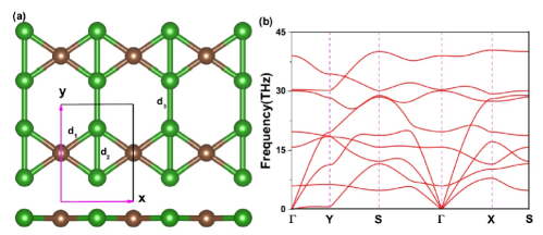
The intrinsic 2D B2C enjoy low buckled configuration between B and C sublattice. The vertical distance between them is 0.025 Å, which is less than previous reportsWu et al. (2009); Dai et al. (2012). The crystal constants along x and y direction are 2.58 Å and 3.42 Å, respectively. All bond lengths labeled in Fig.1(a) are d1 = 1.557 Å, d2 = 1.741 Å, and d3 = 1.683 Å, respectively. The space group of low buckled B2C is Pmm2(No. 25) with the point group C2v, in which only 2-fold rotation along z axis and two mirror symmetries (they are perpendicular to x and y axis) exist. According to the Bader charge analysisHenkelman et al. (2006), C atom obtains 0.1 —e— from two equivalent B atoms. The thermodynamic stability have been proved by previous workWu et al. (2009). They predicted the melt point of B2C monolayer between 2000 and 2500 K with first-principles molecular dynamic computation. To prove the dynamic stability of low buckled B2C, we calculate the phonon dispersion along high symmetry lines and present the result in Fig.1(b). The results show that there is not imaginary frequency in the reciprocal space, therefore, B2C is dynamically stable.
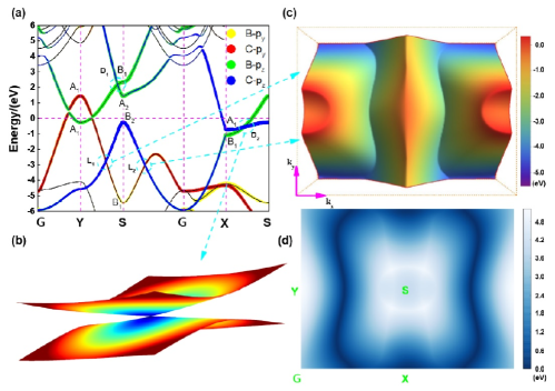
We present the orbit-projected energy band for low buckled B2C in Fig.2(a). The result clearly reveals that the electronic states of low buckled B2C around Fermi level are mainly decided by the B-py,z and C-py,z. For the electronic states near the Fermi level around Y point, the electron-like conduction band originates from B-pz orbitals, whereas the hole-like valence band derives from C-py. There are small band gaps along high symmetry line due to the interaction of these two orbits (both of them show same irreducible representations (IR) of A1). Moreover, there are several energy band crossings for the low energy electronic states along the high symmetry lines, we labeled them as D1, D2, L1, and L2 in Fig.2(a). The point group of point in reciprocal space for low buckled B2C is C2v with two mirror symmetry planes that is perpendicular to the 2D plane. All the k-point in high symmetry line -X, -Y, X-S, and Y-S are share the same point group: Cs. As for such point group, there are only two IRs of A and A, and their mirror operator eigenvalues are opposite. If two energy bands with different IR along the four high symmetry lines as mentioned above, the band cross would unavoidable produces semimetal state. The analysis of the IR of all the four band crossings D1, D2, L1, and L2 indicates that all of them meet the requirement behaving as semimetal. Considering the symmetry of the k-points of the crossings, these four semimetal states are all protected by the mirror symmetry. The 3D energy bands around the band crossing points indicate that D1 is type-I Dirac point and D2 is the latest reported type-II Dirac cone with the broken Lorentz invariance. The 3D energy band of the type-II Dirac cone is shown in Fig.2(b). Two recent works reported that this topological Dirac (type-I and type-II) points can also be realized in photonic systems under special nonsymmorphic symmetryWang et al. (arXiv:1608.02437, 2016, arXiv:1703.09899, 2017), which provide an feasible way to adjust this topological semimetal states.
Intriguingly, the band crossing points of L1 and L2 in the 3D energy bands as shown in Fig.2(c) and (d) (the position of black lines in Fig.2(d) represent the zero gap location of the open type nodal line in 2D reciprocal space) indicate that they expand to the edge of the first Brillouin zone and form a novel open type nodal line semimetal, which is recently proposed in three dimensional materials with special space-group symmetry and time-reversal symmetryTakahashi et al. (arXiv:1704.02151, 2017). However, the dimensions of materials and origin of open nodal line are totally different in these two cases. For B2C, it is two dimensional materials and it’s open nodal lines mainly come from strong anisotropic in-plane interaction. The IRs of these two bands around the high symmetry point S are B1 and B2 showing opposite mirror eigenvalues. Moreover, the two bands inverse around the S point between L1 and L2. Such energy band inversion shows strong in-plane anisotropic between x and y directions. The anisotropy produces the energy band crossing points on both sides of line X- unconnected each other along kx orientation and form two separate open type nodal line. The work of Takahashi et alTakahashi et al. (arXiv:1704.02151, 2017) concentrate on how nodal line appears under special non-symmorphic symmetry, and they proved that open nodal line may come from exchange glide eigenvalues between two high-symmetry lines. It must be emphasized that the open nodal lines mainly mean energy band crossing lines around high symmetry point do not form closed ring in first Brillouin zone which is independent of the choice of the Brillouin zones.
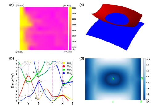
As mentioned above, the fluctuation between B and C sublattices of low buckled B2C is very small (0.025 Å), and this z-direction fluctuation can be removed by applying tiny stretching strain. Although, the phonon spectrum as shown in Fig.S1 in the supplementary materials indicates that the isolated flat B2C is dynamically instable, the pure flat B2C can be realized on appropriate substrate or curved substrate. In the following part, we will study the electronic structures of isolated pure flat B2C, and the substrate will be discussed below. The distance h between B and C sublattices along z-direction in function of the stretching strain in x- and y-directions is shown in Fig.3(a). The results indicate that when the strain along x orientation is larger than 2%, the h is close to zero (The magenta zone in the figure represents h can be neglected). The results indicate that with stretching strain, the low buckled B2C can be feasibly produced to pure flat one. The space group of flat B2C change to Pmmm (No. 47) with the point group D2h. The band structure of pure flat B2C is shown in Fig.3. In comparison with that of low buckled system, the type-I and type-II Dirac point as well as the open type nodal line around S point in low buckled B2C are all reserved in the flat system. However, the two gaps around Y point of the low buckled B2C near Fermi level are all closed. The 3D energy band around Y point in reciprocal space as shown in Fig.3(c) indicates that the bands form a nodal loop around Y point. In the figure, the red and blue curved surfaces represent the bands contributed by B-pz and C-py, respectively. With the help of group analysis, we find that the point group of four time inversion invariance point in reciprocal space of low buckled B2C is turned to D2h for the flat B2C. In this point group, all three coordinate axes are two-fold rotation axis. As shown in Fig.3(a), the IR of the two energy bands near Fermi level around Y point are B1u and Ag now, respectively. Under the operator of spatial inversion symmetry, the parity of the wavefunctions of these two bands are opposite, meanwhile, time-reversal symmetry always exists in low buckled or flat B2C. Therefore, the wavefunctions can not interact with each other around the Y producing the gaps close and then forming nodal line around this point. Namely, for the flat B2C, the nodal loop around Y point is protected by the spatial inversion symmetry and time-reversal symmetry at the same time, which prohibit the interaction between pz and py states..
Here we will firstly discuss the origin of the topological properties of Dirac semimetal states of D1 and D2. Under the time-reversal symmetry () and spatial inversion symmetry(), the Zak phase is quantized and topological analysis is meaningfulvan Miert et al. (2017), therefore, we concentrate on the case of flat B2C. According to previous workvan Miert et al. (2017), 2D semimetal states can be divided into two categories: trivial and non-trivial Z2 invariant semimetal. They are decided by the parity of occupied Bloch wave function at points. The Dirac semimetal states D1 and D2 of 2D B2C are formed by the crossing of two bands with different parity as shown in Fig.3(b), their topological properties should be contributed by the parity of the two bands in reciprocal space. In the unit cell of B2C, two B atoms and one C atom contribute totally ten electrons. Ignoring the freedom of spin, ten valence electrons will occupy five lowest energy bands. For the two crossing bands of D1 and D2, we assume the band whose energy is higher than the other belongs to the conduction band. According to the work of Miert et alvan Miert et al. (2017), if the Dirac point locate in the high symmetry lines with two time-reversal invariant terminals, the quantized Zak phase can be simplified as the parity of the full Bloch wave function at the time-reversal invariant points. The concrete formula is:
| (1) |
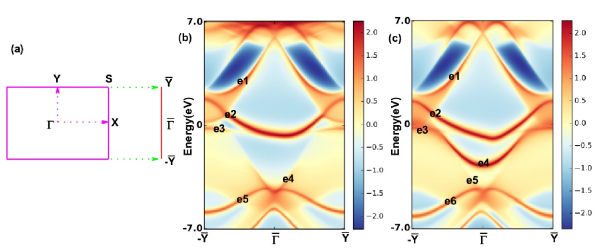
where is the occupied energy band, and represent the beginning and the ending point of any high symmetry line, respectively, for with one Dirac point on it. For D2, the high symmetry line is X-S, then the and are X and S points, respectively. However, for the case of D1, the high symmetry line is Y-S, and the and indicate Y and S high symmetry points, respectively. The result of Eq.1 is -1(1) indicating the system topological non-trivial(trivial). As for D2, the parities of valence bands at X and S high symmetry point are (+1, -1, -1, -1, +1) and (+1, -1, +1, -1, +1), respectively. The parities of valence bands at Y and S for D1 are (-1, +1, +1, +1, -1, +1) and (+1, -1, +1, -1, +1, -1), respectively. Based on Eq.1, both D1 and D2 semimetal states are topological non-trivial, which also are proved by our further Berry phase calculation around these two points. If we adapt the anticlockwise circular k-path in reciprocal space, the Berry phase of D1 and D2 are and -, respectively. To further prove the topological nature of these semimetals states, we calculated the edge states with the Green’s function method and semi-infinite MLWF Hamiltonian. The results for low buckled and flat B2C are shown in Fig.4 (b) and (c), respectively. All edge states around Fermi level are labeled as e1 to e6 in Fig.4(c). By comparing the number of edge states between Fig.4(b) and Fig.4(c), e4 is the edge state of closed nodal line in flat B2C. According the energy range of other semimetal states as shown in Fig.2(a) and Fig.3(b), we can sum up the correspondence between these edge states and semimetal states as: e1 D1, e3 D2, e5 L1(L2). However, after analyzing the edge states in detail with different symmetry, we found the e2 and e6 are a normal trivial edge states derived from the symmetric broken of the ribbon edge.
In this part, we derive the effective model to two different type nodal line of flat B2C. Generally, a two-band model can be written as following formYu et al. (2016):
| (2) |
where is 2 2 unit matrix, and are Pauli Matrices. (k) denote real function of k(kx,ky). Under space-inversion symmetry operator P̂ and time-reversal symmetry operator T̂, the effective Hamiltonian must satisfy
| (3) |
Because the two bands we considered own opposite parity if omit the freedom of spin, hence the operator P̂ and T̂ can be chosen as and K. K represents the complex-conjugate operator. After substituting them into above formula, we can obtain that = 0, is an odd function of k and are even functions of k. Moreover, two additional mirror symmetries would require the Hamiltonian satisfying: kx -kx; ky -ky. If we only expand the Hamiltonian to two order of k, we have
| (4) | |||
| (5) | |||
| (6) |
Because the only breaks the particle-hole symmetry and affects the energy dispersion of the nodal line, we only need to consider the case of = 0. The parameters , , and of are independent each other due to no additional symmetry restriction. When and have opposite signs, the equation is equivalent to ellipse equation (). If the length of the two principal axes ( and ) of the ellipse are both shorter than corresponding basis vector of 2D reciprocal space, a nodal loop will form. The closed nodal line around Y point for flat B2C is the case. If the length of any principal axis of the ellipse is longer than corresponding primitive vector, two non-closed nodal lines would be formed, this is the case of open type nodal lines in both low buckled and flat B2C. It is worth noting that there is a third case that the length of all principal axis of the ellipse are longer than corresponding primitive vector and one of them is shorter than the diagonal of the 2D rectangle Brillouin zone. In such case, four separated nodal lines will form in the first Brillouin Zone, which is very similar with the 2D boundary plane of Cu3NPdKim et al. (2015), even though it is 3D materials. Below, we will use TB Hamiltonian to explain the formation of the two types nodal lines in B2C.
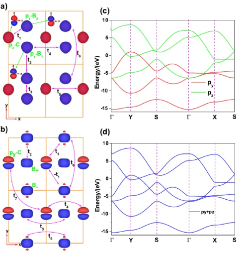
According to the atom-projected energy bands around Fermi level as shown in Fig.2(a) and Fig.3(b), we know that the low energy electronic states mainly come from py and pz states of B and C atoms. To understand the formation of semimetal states in 2D B2C, we can construct a six-band TB model with the help of MLWFs. The hamiltonian can be written as:
where and are constructed with the basis of py and pz states of all atoms, respectively. is the perturbation to describe the interaction between py and pz states. For pz states, the center of Wannier function locates near the position of atoms, therefore, the basis of them can be set as traditional TB model (pz-C, pz-B1, and pz-B2) as shown in Fig.5(a). However, the py states of B atoms interact with each other and form bonding (py-B1 + py-B2) B+ and antibonding (py-B1 - py-B2) B- due to the mirror symmetry. The bonding state center locates at the midpoint between B1 and B2 atoms, whereas the antibonding state center is at the midpoint of primitive vector along x-axis as shown in Fig.5(b). Therefore, the basis can be set as (py-C,B+, and B-). With the two basis, the and in TB model can be formulated as follows:
| (7) |
where n = 1 (2) represent the three bands model with the basis of py (pz) orbits, is on-site energy, () represents the creation (annihilation) operator of electrons at site i (j). ( = 1-7 for py model and = 1-6 for pz model) are the hopping parameter between the i-th and j-th sites. The details of the parameters used in our present work can be found in the Tab.S1 in the supplementary materials. When is 3 3 zero matrix, namely the interactions between py and pz orbits are omitted, we plot the band structure of in Fig.5(c). The red and green lines are, respectively, come from the eigenvalues of and and they are well match with the first-principles energy band of Fig.3(b). When we add a weak interaction between py and pz orbits, band gap will open for the nodal line around Y high symmetry point. Here we take the interaction parameter of -0.1 between B- and its nearest neighbor pz-B1 or pz-B2 as an example, and the band structures along high symmetry lines are shown in Fig.5(d). Clearly, local band gaps open for the closed nodal line around Y. With the help of energy band structures derived from TB model, we can draw the following conclusions: The two types of nodal lines in flat B2C come from the energy band crossing between py and pz orbits, but the two Dirac semimetal states are only derived from pz orbitals. The disappearance of the interaction between py and pz orbits for flat B2C can well describe the existence of the closed nodal line around Y point. Moreover, whether or not matrix exists, the interaction between these two types of orbitals would not break the mirror symmetry along x and y axis. Therefore, the open type nodal line and two Dirac semimetal states are all determined by the mirror symmetries and independent of .
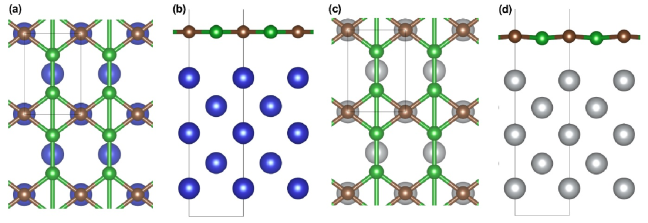
Now, we will discuss the proper substrate to synthesize the monolayer B2C. It is well known that crystal constant matching between substrates and 2D materials is an important prerequisite for synthesizing monolayer 2D materials. By comparing the crystal constants between different metal surface and B2C, we find that the crystal constants of B2C match well with Cu(110) surface (the mismatches are -0.95% and 5.2% in x and y orientations, respectively) and Ni(110) surface (the mismatches are -3.5% and 2.8% in x and y orientations, respectively, where the negative percentage mean the lattice constant of substrate is shorter than corresponding lattice constant of low buckled B2C.). To obtain the most stable B2C structure by self-assembled process on these two metal surfaces, we adapt the recently developed surface reconstruction prediction methodLu et al. (2014) based on particle swarm optimization (PSO)Wang et al. (2010), which has been recently utilized to simulate the growth of monolayer borophene on different metal substrateZhang et al. (2015). The most stable B2C on the surface of Cu(110) and Ni(110) are present in the Fig.6. The results indicate that the fundamental structure of 2D B2C is well reserved in comparison with free standing monolayer film. The buckle between B and C sublattice of B2C is negligible when it on the surface of Cu(110) realizing the flat B2C. However, when it on the surface of Ni(110), the buckle reaches 0.127 Å obtaining the buckled B2C. We also present other typical adsorption structures on the surface of Cu(110) with higher energy in Fig.S2 in the supplementary materials. Although the results indicate that the B or C atoms on the grooves of Cu(110) or Ni(110) surface are not energy favorable, the energy difference between different adsorption configurations are within several meV. The above results indicate that the Cu(110) or Ni(110) surfaces are promising substrate for growing the monolayer B2C. However, the pz states of B and C atoms are largely affected due to the interaction between B2C and metal substrate, by which the topological properties of the systems can not be reserved. To guarantee the topological metal states, we construct a van der Waals bilayer B2C on the surface of the substrate, the detailed electronic structure analysis are presented in Fig.S3 in the supplementary materials. The projected energy bands of the superficial B2C indicate that the topological metal states are well reserved.
The most interesting nature of B2C is that its different type semimetal states around Fermi level locate different energy windows, that can be easily distinguished in experiments. Nowadays, the nodal line semimetal state was only indirectly observed in 3D materials in experiments with angle-resolved photoemission spectroscopy (ARPES), which is largely affected by the orientation and termination of the surface. Therefore, we expect the 2D B2C would be the choice example to directly observe the state of nodal line semimetal. Moreover, for low buckled B2C, there are three types semimetal states coexistence (including type-I and type-II Dirac semimetal and open type nodal line semimetals), whereas for flat B2C, there are four types semimetal states simultaneous existence (including type-I and type-II Dirac semimetal and open and close type nodal line semimetals). All the coexisting semimetal states located at different momenta might couple to each other through electron interactions, namely, the B2C system will provide an excellent platform for studying the interplay between different types semimetals.
In summary, we have found four semimetal states coexist in the low energy electronic state of 2D B2C with negligible SOC. These semimetal states are protected by , , or mirror symmetry. It is worth mentioning that the open type nodal line is firstly proposed in 2D materials, and it is rooted in the strong in-plane anisotropy interaction. Two band effective model and six-orbital TB model have been constructed to describe the details of anisotropy interaction and the origin of topological semimetal states. The different types semimetal states of 2D B2C around Fermi level locate different energy window that can be easily distinguished in experiments. Moreover, the system provides an excellent platform for studying the interplay between different types semimetals.
Acknowledgements.
This work is supported by the National Natural Science Foundation of China (Grant No. 11574260) and scientific research innovation project of Hunan Province(CX2015B219).References
- Hasan and Kane (2010) Hasan, M. Z.; Kane, C. L. Rev. Mod. Phys. 2010, 82, 3045–3067
- Qi and Zhang (2011) Qi, X.-L.; Zhang, S.-C. Rev. Mod. Phys. 2011, 83, 1057–1110
- Wehling et al. (2014) Wehling, T.; Black-Schaffer, A.; Balatsky, A. Adv. Phys. 2014, 63, 1–76
- Xu et al. (2015) Xu, S.-Y. et al. Science 2015, 349, 613–617
- Lu et al. (2015) Lu, L.; Wang, Z.; Ye, D.; Ran, L.; Fu, L.; Joannopoulos, J. D.; Soljačić, M. Science 2015, 349, 622–624
- Lv et al. (2015) Lv, B. Q.; Weng, H. M.; Fu, B. B.; Wang, X. P.; Miao, H.; Ma, J.; Richard, P.; Huang, X. C.; Zhao, L. X.; Chen, G. F.; Fang, Z.; Dai, X.; Qian, T.; Ding, H. Phys. Rev. X 2015, 5, 031013
- Son and Spivak (2013) Son, D. T.; Spivak, B. Z. Phys. Rev. B 2013, 88, 104412
- Vazifeh and Franz (2013) Vazifeh, M. M.; Franz, M. Phys. Rev. Lett. 2013, 111, 027201
- Soluyanov et al. (2015) Soluyanov, A. A.; Gresch, D.; Wang, Z.; Wu, Q.; Troyer, M.; Dai, X.; Bernevig, B. A. Nature 2015, 527, 495–498
- Huang et al. (2016) Huang, H.; Zhou, S.; Duan, W. Phys. Rev. B 2016, 94, 121117
- Guo et al. (2017) Guo, P.-J.; Yang, H.-C.; Liu, K.; Lu, Z.-Y. Phys. Rev. B 2017, 95, 155112
- Chang et al. (arXiv:1606.07555, 2016) Chang, T.-R. et al. Type-II Topological Dirac Semimetals: Theory and Materials Prediction (VAl3 family). arXiv:1606.07555, 2016
- Weng et al. (2015) Weng, H.; Liang, Y.; Xu, Q.; Yu, R.; Fang, Z.; Dai, X.; Kawazoe, Y. Phys. Rev. B 2015, 92, 045108
- Yu et al. (2015) Yu, R.; Weng, H.; Fang, Z.; Dai, X.; Hu, X. Phys. Rev. Lett. 2015, 115, 036807
- Yu et al. (2016) Yu, R.; Fang, Z.; Dai, X.; Weng, H. Front. Phys. 2016, 12, 127202
- Bian et al. (2016) Bian, G. et al. Nat. Commun. 2016, 7, 10556
- Wu et al. (2016) Wu, Y.; Wang, L.-L.; Mun, E.; Johnson, D. D.; Mou, D.; Huang, L.; Lee, Y.; Bud’ko, S. L.; Canfield, P. C.; Kaminski, A. Nat. Phys. 2016, 12, 667–671
- Schoop et al. (2016) Schoop, L. M.; Ali, M. N.; Straer, C.; Topp, A.; Varykhalov, A.; Marchenko, D.; Duppel, V.; Parkin, S. S. P.; Lotsch, B. V.; Ast, C. R. Nat. Commun. 2016, 7, 11696
- Lu et al. (arXiv:1603.04596, 2016) Lu, J. L.; Luo, W.; Li, X. Y.; Yang, S. Q.; Cao, J. X.; Gong, X. G.; Xiang, H. J. Two-Dimensional Node-Line Semimetals in a Honeycomb-Kagome Lattice. arXiv:1603.04596, 2016
- Jin et al. (arXiv:1608.05791, 2016) Jin, Y.; Wang, R.; Zhao, J.; Zheng, C.; Gan, L.-Y.; Liu, J.; Xu, H.; Tong, S. Y. A Family Group of Two-dimensional Node-Line Semimetals. arXiv:1608.05791, 2016
- Yang et al. (arXiv:1612.06562, 2016) Yang, B.; Zhang, X.; Zhao, M. Dirac node lines in a two-dimensional bipartite square lattice. arXiv:1612.06562, 2016
- Niu et al. (arXiv:1703.05540, 2017) Niu, C.; Buh, P. M.; Zhang, H.; Bihlmayer, G.; Wortmann, D.; Bl gel, S.; Mokrousov, Y. Topological Nodal-line Semimetals in Two Dimensions with time-reversal symmetry breaking. arXiv:1703.05540, 2017
- Kresse and Hafner (1993) Kresse, G.; Hafner, J. Phys. Rev. B 1993, 47, 558–561
- Kresse and Furthmüller (1996) Kresse, G.; Furthmüller, J. Phys. Rev. B 1996, 54, 11169–11186
- J. Klimes (2010) J. Klimes, A. M., D.R. Bowler J. Phys.: Condens. Mat. 2010, 22, 022201
- Klimeš et al. (2011) Klimeš, J. c. v.; Bowler, D. R.; Michaelides, A. Phys. Rev. B 2011, 83, 195131
- Togo and Tanaka (2015) Togo, A.; Tanaka, I. Scr. Mater. 2015, 108, 1–5
- Wu et al. (arXiv:1703.07789, 2017) Wu, Q.; Zhang, S.; Song, H.-F.; Troyer, M.; Soluyanov, A. A. WannierTools: An open-source software package for novel topological materials. arXiv:1703.07789, 2017
- Mostofi et al. (2008) Mostofi, A. A.; Yates, J. R.; Lee, Y.-S.; Souza, I.; Vanderbilt, D.; Marzari, N. Comput. Phys. Commun. 2008, 178, 685 – 699
- Wu et al. (2009) Wu, X.; Pei, Y.; Zeng, X. C. Nano Lett. 2009, 9, 1577–1582
- Dai et al. (2012) Dai, J.; Li, Z.; Yang, J.; Hou, J. Nanoscale 2012, 4, 3032–3035
- Henkelman et al. (2006) Henkelman, G.; Arnaldsson, A.; Jnsson, H. Comp. Mater. Sci. 2006, 36, 354 – 360
- Wang et al. (arXiv:1608.02437, 2016) Wang, H.-X.; Chen, Y.; Hang, Z. H.; Chen, H.; Kee, H.-Y.; Jiang, J.-H. 3D Z2 Topological Nodes in Nonsymmorphic Photonic Crystals: Ultrastrong Coupling and Anomalous Refraction. arXiv:1608.02437, 2016
- Wang et al. (arXiv:1703.09899, 2017) Wang, H.-X.; Chen, Y.; Hang, Z. H.; Kee, H.-Y.; Jiang, J.-H. Type-II Dirac Photons. arXiv:1703.09899, 2017
- Takahashi et al. (arXiv:1704.02151, 2017) Takahashi, R.; Hirayama, M.; Murakami, S. Topological nodal-line semimetals arising from crystal symmetry. arXiv:1704.02151, 2017
- van Miert et al. (2017) van Miert, G.; Ortix, C.; Smith, C. M. 2D Mater. 2017, 4, 015023
- Kim et al. (2015) Kim, Y.; Wieder, B. J.; Kane, C. L.; Rappe, A. M. Phys. Rev. Lett. 2015, 115, 036806
- Lu et al. (2014) Lu, S.; Wang, Y.; Liu, H.; Miao, M.-s.; Ma, Y. Nat. Commun. 2014, 5, 3666
- Wang et al. (2010) Wang, Y.; Lv, J.; Zhu, L.; Ma, Y. Phys. Rev. B 2010, 82, 094116
- Zhang et al. (2015) Zhang, Z.; Yang, Y.; Gao, G.; Yakobson, B. I. Angew. Chem. Int. Edit. 2015, 54, 13022–13026