Thermal conductivity reduction in rough silicon nanomembranes
Abstract
Nanostructured silicon is a promising material for thermoelectric conversion, because the thermal conductivity in silicon nanostructures can be strongly reduced with respect to that of bulk materials. We present thermal conductivity measurements, performed with the 3 technique, of suspended monocrystalline silicon thin films (nanomembranes or nanoribbons) with smooth and rough surfaces. We find evidence for a significant effect of surface roughness on phonon propagation: the measured thermal conductivity for the rough structures is well below that predicted by theoretical models which take into account diffusive scattering on the nanostructure walls. Conversely, the electrical conductivity appears to be substantially unaffected by surface roughness: the measured resistance of smooth and rough nanostructures are comparable, if we take into account the geometrical factors. Nanomembranes are more easily integrable in large area devices with respect to nanowires and are mechanically stronger and able to handle much larger electrical currents (thus enabling the fabrication of thermoelectric devices that can supply higher power levels with respect to current existing solutions).
I Introduction
In the last years, significant research effort has been devoted to the investigation of thermal transport in nanostructures, such as silicon nanowiresLi et al. (2003); Hochbaum et al. (2008); Pennelli et al. (2014). It has been found that their thermal conductivity is often rather small, because phonon propagation is suppressed by scattering on the nanowire surfaces. As demonstrated by several experimental investigationsLim et al. (2012); Park et al. (2011); Feser et al. (2012); Kim et al. (2011), and confirmed by theoretical considerationsMartin et al. (2009); Liu and Chen (2010); Carrete et al. (2011), rough surfaces do suppress phonon conduction: values of thermal conductivity down by two orders of magnitude with respect to that of bulk silicon can in principle be achieved. The key point is that, in order to achieve satisfactory operation of thermoelectric devices, the electrical conductivity must instead be minimally affected by surface roughness. Suppression of thermal conductivity while keeping a good electrical conductivity opens up interesting opportunities in the field of energy harvesting, because a high thermoelectric conversion efficiency could be achieved with a material, such as silicon, abundant on the Earth’s crust and biocompatible. Since single nanostructures can handle only a limited amount of current, a thermoelectric generator (TG) useful for practical applications must consist in a large collection of interconnected nanostructuresPennelli et al. (2013); Totaro et al. (2012); Davila et al. (2012). Silicon nanomembranes and nanoribbons, with one dimension (thickness) much smaller than the other (width ) represent an interesting alternative to nanowires, since a very large number of them can be packed in parallelPennelli and Macucci (2016) with the larger side perpendicular to the surface. Although the nanomembrane approach is promising for practical TGs, it is expected that the thermal conductivity suppression with decreasing nanomembrane thickness could be less effective than in nanowiresMarconnet et al. (2013). Our study is aimed at understanding how far surface roughness can go in reducing thermal conductivity of nanomembranes.
We developed a process for the fabrication of suspended silicon nanoribbons, together with contacts for the in-plane electrical characterization and a heater for 3 in-plane thermal transport characterization. We measured the electrical and thermal transport of smooth nanoribbons, and compared them with that of rough ones. Roughness was characterized by means of AFM imaging. Thermal conductivity measurements are compared with simple theoretical models, based on the assumption of fully diffusive phonon scattering on the nanomembrane walls. A strong reduction of the thermal conductivity in thin nanomembranes, with respect to that predicted by diffusive models, is demonstrated. Specific models for the phonon propagation in rough nanomembranes, which demonstrates these experimental results, still need to be developed.
II Device fabrication
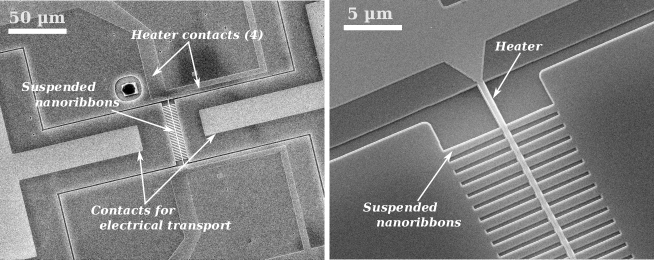
The left panel of Fig. 1 shows a SEM image of a typical device,
made up of an array of suspended thin silicon membranes, arranged in a double
comb configuration with a central
silicon body. On this silicon body, a metal (gold) strip is the
heater for the 3 thermal conductivity measurement. The resistance
of this metal strip can be measured by means of leads arranged
in a four contact configuration. Another couple of contacts allow the
measurement of the electrical conductivity
of the silicon nanomembranes.
The device has been fabricated on the top silicon layer of a Silicon On
Insulator substrate. The top silicon layer is
260 nm thick, the buried oxide layer is 1 m thick and the total substrate
thickness is 0.5 mm. The process is
similar to that already used for the fabrication of silicon nanowire
devicesCiucci et al. (2005); Pennelli et al. (2006); Pennelli and Pellegrini (2007), and is based
on electron beam
lithographyPennelli et al. (2003) and silicon anisotropic etching. An eventual
thinning of the top silicon layer is performed by dry oxidation and BHF etching.
The thicknesses have been measured from Atomic Force
Microscopy (AFM) images, taken during the process steps.
The process steps can be summarized as follows.
1) A 40 nm thick SiO2 layer
is grown on the top silicon layer.
2) Electron beam lithography is used for the definition of trenches in the
top SiO2 layer,
with the deposition of PMMA resist, e-beam exposure, development,
and SiO2 etching by means of Buffered HF (BHF).
In this step,
the comb geometry is defined in the top SiO2 layer. After BHF etching,
the thickness of the top SiO2 layer has been measured, with a result around 40 nm
for all the fabricated samples.
3) KOH etching has then been used for transferring this pattern to the
top silicon layer. After this step, AFM imaging
has been performed for the measurement of the thickness of the top silicon
plus the top SiO2 layer. Therefore, the
top silicon layer thickness has been obtained by subtracting the
SiO2 thickness, measured before
the KOH etching, as KOH has practically no effect on SiO2. A final
nanomembrane thickness of 240 nm has been measured, if the process
is performed on the substrate with a top silicon layer 260 nm thick. Different
thicknesses (see the measurement results) have been achieved by thinning the
substrate through oxidation/BHF etch before the first lithographic step.
4) Then the top silicon dioxide layer has been removed by means of BHF
etching. This etch step allows the
deposition of the metal tracks in direct contact with silicon, without any
insulating layer in between.
5) An e-beam lithography step has then been performed on a PMMA double layer,
and then a metal layer, consisting of 10 nm of Chromium
for adhesion and of of 80 nm of Gold, has been deposited by means of
thermal evaporation. Metal lift off has been performed in hot acetone.
This lithographic step has
been carefully aligned with the
comb structure underneath, so that the metal track has been positioned exactly
on the silicon body in the middle of the device.
6) The nanomembranes (both the comb and the central body) have been suspended
by underetching the buried oxide by means of BHF.
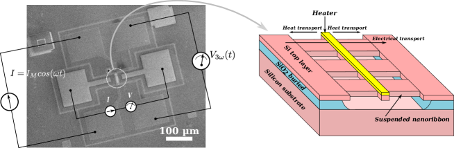
The final device is shown in Fig. 2, together with a sketch
of the suspended structures.
The sketch, drawn on the SEM photo, illustrates the purpose of each contact.
The contacts at the sides of the comb
are used for the measurement of the overall electrical conductivity of the
nanoribbons. The four contacts are used for
the precise measurement of the resistance of the metal strip fabricated in
the middle of the comb.
The nanomembrane roughening is performed after the definition of the metal
track, but before the suspension
of the nanomembranes by means of SiO2 underetching: nanomembranes are
very delicate, and any attempt at roughening suspended
nanostructures has resulted in a very low yield in terms of final number
of working devices.

.
A rough surface has been achieved by soaking the sample in a solution with hydrofluoric acid and silver nitrate; this technique has been already used by LimLim et al. (2012) and coworkers for roughening silicon nanowires. The SEM image of Fig. 3 shows silver nanoparticles, deposited on the surface of a nanomembrane by soaking the sample in a solution AgNO3/HF 0.01/5.1 mol for 60 s. Silver is reduced, withdrawing an electron from silicon (i.e. injecting a hole), so that it precipitates, aggregating in nanoparticles on the silicon surface. The reduced silicon is etched by the hydrofluoric acid. Therefore, a local etching of silicon occurs under the silver nanoparticles. This mechanism is not fully understood yet, even if it is the basis of the Metal Assisted Chemical Etching (MaCE) technique, largely used for the fabrication of silicon nanowires perpendicular to a silicon substrateDimaggio and Pennelli (2016). We use this MaCE technique to produce shallow holes that are randomly distributed on the silicon surface. After the etch step, the silver nanoparticles have been removed by soaking the sample in HNO3: H2O 1:5 for 2 m. The result is a very rough surface, as visible in the SEM image in the bottom panel of Fig. 3. The characteristic of the silicon nanoribbons has been measured before and after the roughening process, through the contacts placed at the sides of the comb, as shown in Fig. 2. In this way, the relationship between the electrical conductivity before and after roughening has been established. An important quantity that must be determined for the evaluation both of the electrical and of the thermal conductivity is the final thickness of the silicon nanomembranes. The roughening process leaves a chaotic pattern on the silicon surface, but it also removes a small amount of silicon, thus reducing the thichness of the nanoribbons. As HF etches the SiO2 buried layer, a direct measurement of the final thickness of the nanomembranes, after the roughening process, is not possible. Therefore, the thickness has been measured using the gold metal tracks as a reference, because gold is substantially unaffected by the etching processes. The thickness of the metal tracks, with respect to the silicon, has been measured by means of AFM imaging before and after the roughening process. The difference between the two measurements corresponds to the amount of silicon that has been removed. Due to the roughness of the silicon surface, an average thickness has been obtained by averaging over areas of several square microns.
The thermal conductivity is evaluated with the 3 technique, exploiting the metal structure fabricated in the middle of the double comb both as a heater and as a temperature sensor. A sinusoidal electrical current is injected into the metal track through two of the four available contacts. The heat generated as a result of the Joule effect can be dissipated only through the nanomembranes in the direction of their plane, because they are suspended. The voltage is measured through the other two available contacts (four-probe configuration), and the amplitude of the third harmonic is extracted by means of a lock-in amplifier (see the sketch on the SEM image of Fig. 2). As it has been demonstrated in several applications, the amplitude of the third harmonic is related to the thermal dissipationCahill (1990); Lu et al. (2001); Jain (2008), which in our case is due to the thermal conductivity in the film plane. For the proper application of the 3 technique it is essential to choose the correct model for data reduction. Although an analytical model has been developed for 2D structuresJain (2008) (thin membranes), in our case we have fitted the data by means of an approach based on FEM (Finite Element Method) simulations that we have developed Pennelli et al. (2017), using the thermal conductivity as a fitting parameter. The simulation takes into account the thermoelectric transport in the metal and in the silicon nanostructures, considering the measured electrical conductivities.
III Thermal and electrical conductivities
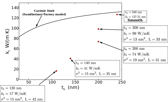
In Fig. 4 the results of the measured thermal conductivity of smooth and rough silicon nanomembranes are shown. On the same plot, the thermal conductivity predicted by means of a theoretical model is also reported for comparison purposes. The theoretical evaluation of the thermal conductivity has been performed following the Callaway-Holland formalismJ.Callaway (1958); M.G.Holland (1963), in the vision developed by Asen-PalmerAsen-Palmer et al. (1997) and, in particular, from the expression by Morelli et al.Morelli et al. (2002):
| (1) |
where is the Debye temperature, is the reduced Planck constant, is the absolute temperature, is the Boltzmann constant, , and is the relaxation time. Both the contribution of due to the longitudinal mode and that of due to the transverse phonon modes have been evaluated taking into account the proper parameters, for example considering K and K for the Debye temperatures of the longitudinal and transverse phonons, respectively. The two contributions have then been combined to derive the total thermal conductivity: .
In the evaluation of the relaxation time , we have taken into account the contribution of different scattering processes, combining them by means of Matiessen’s rule.
The relaxation times , relative to the phonon-phonon normal scattering, , relative to the phonon umklapp scattering and , relative to the isotope scattering, have been evaluated using the parameters reported by Morelli et al. Morelli et al. (2002) for the longitudinal and the transverse phonon modes. Several models have been developed in the literature for the inclusion of the phonon boundary scattering, which is a phenomenon of fundamental importance for the accurate evaluation of the thermal conductivity in nanostructures. In our model we have considered completely diffusive boundary scattering, so that the resulting thermal conductivity is the one corresponding to the so-called Casimir limit. In order to include also the contribution from boundary scattering, we followed an approach similar to the one proposed by SondheimerSondheimer (1952) for the electrical conduction in thin metal films, based on the solution of the Boltzmann transport equation. For the present work, we have used the simpler solution developed by Turney et al.Turney et al. (2010) for phonon transport in thin silicon layers with a width much greater than the thickness . Following this model, at first a preliminary relaxation time has been computed with Mathiessen’s rule, including all the scattering phenomena, but the phonon boundary scattering. Then, the total relaxation time has been evaluated as (see the paper by Turney et al.Turney et al. (2010), with the probability of thermalised boundary scattering ):
| (2) |
where ( is for longitudinal and for transverse phonon).
In Fig. 4 the continuous line represents the thus computed thermal conductivity as a function of the thickness , for a silicon nanoribbon 1 m wide, which is a width comparable to that of our devices. It is possible to see that with the adopted model exhibits a moderate dependence on the thickness of the nanoribbon, because the mean free path for boundary scattering is mainly determined by the nanoribbon width rather than the thickness, as already reported by Wang and MingoWang and Mingo (2011). The experimental value reported at the top right of Fig. 4 has been obtained on a 240 nm thick smooth nanoribbon, and it appears to be in good agreement with the theoretical prediction. Indeed at the end of the fabrication process the nanoribbons are very smooth if the roughening step has not been performed. The oxidation step used for the definition of the mask for silicon etching preserves the smoothness of the surface, while reducing the thickness of the nanoribbons, whose final value is 240 nm (from AFM measurements).
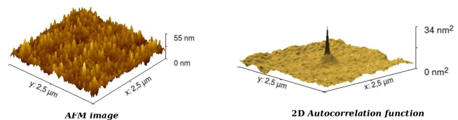
The thermal conductivity undergoes a dramatic change if the roughening process (described in the previous Section) is performed. The AFM image in the left panel of Figure 5 shows the surface after the roughening process. In the right panel we report the two-dimensional autocorrelation function of the same image, from which the main characteristics of the roughness can be derived. In particular, the autocorrelation function has been fitted with a gaussian: , where is the standard deviation with respect to the average value of the surface and is the autocorrelation parameter. For the sample shown in Fig. 5 we achieved nm2 and nm. Part of the silicon is etched during the roughening process, therefore at the end the final thickness of the nanomembranes is reduced: the final thickness is measured by means of AFM imaging, as explained in the previous section.
For a final thickness of 200 nm we report the values of the thermal conductivity for two different values of the roughness variance: while for nm2 we get 99 W/(m K), for nm2 is reduced down to 74 W/(m K). As the thickness is decreased we observe, for similar values of the roughness, a sharp decrease of the thermal conductivity, down to 17 W/(m K) for nm. This is analogous to what has been measuredLi et al. (2003); Hochbaum et al. (2008); Pennelli et al. (2014); Lim et al. (2012); Park et al. (2011); Feser et al. (2012); Kim et al. (2011) and theoretically predictedMartin et al. (2009); Liu and Chen (2010); Carrete et al. (2011) for silicon nanowires.
It must be noted that the roughening step must be performed before
the underetch of the buried oxide, which is needed to achieve the
suspension of the nanomembranes.
Therefore, we cannot measure the thermal conductivity before and after
the roughening process, and the values reported in Fig. 4
have been obtained on different samples.
The electrical resistance
has been measured through the electrical contacts fabricated
at the sides of the suspended nanoribbons (see Fig. 1).
The top silicon layer has an uniform doping of cm-3.
We report, as a typical example, the resistance of the sample with smooth
nanoribbons 240 nm thick: the resistance was . For the
rough sample, with nanoribbons 120 nm thick, we measured an the electrical
resistance of : this is compatible with the final
thickness of the sample (120 nm), and with the slight reduction of the
nanoribbon width as a consequence of silicon etching associated with roughening.
Therefore, the final measured resistance is consistent with the variation
of the geometrical parameters (thickness and width), and this
means that the electrical conductivity is practically unchanged. Both
resistance values, taking into account the geometrical factors, give an
electrical conductivity of 0.006 . This value is
compatible with the nanoribbon doping.
This is a key point for future applications of the monocrystalline nanoribbons for thermal to electrical energy conversion: the thermal conductivity is strongly reduced by the rough surface, while the electrical conductivity is practically unaffected.
IV conclusions
We have presented an application of the particular version of the 3 technique that we have developed for the evaluation of the thermal conductivity of rough suspended silicon nanomembranes, for which a direct application of the commonly used analytical approximations would lead to excessive approximations. While in the absence of significant surface roughness the results of our measurements are in agreement with theoretical predictions, the introduction of roughness appears to strongly suppress thermal conductivity, in analogy with what has been previously observed in the literature for silicon nanowires, while substantially leaving the electrical conductivity unaffected. If confirmed, this would make rough silicon nanoribbons quite interesting candidates for silicon-based thermoelectric generators, because of the relatively high figure of merit and the current carrying capability, which is significantly larger than that of silicon nanowires.
References
- Li et al. (2003) Li, D.; Wu, Y.; Kim, P.; Shi, L.; Yang, P.; Majumdar, A. Thermal Conductivity of Individual Silicon Nanowires. Appl. Phys. Lett. 2003, 83, 2934–2936.
- Hochbaum et al. (2008) Hochbaum, A. I.; Chen, R.; Delgrado, R. D.; Liang, W.; Garnett, C. E.; Najarian, M.; Majumdar, A.; Yang, P. Enhanced Thermoelectric Performance of Rough Silicon Nanowires. Nature Letters 2008, 451, 163–167.
- Pennelli et al. (2014) Pennelli, G.; Nannini, A.; Macucci, M. Indirect Measurement of Thermal Conductivity in Silicon Nanowires. J. Appl. Phys. 2014, 115, 084507.
- Lim et al. (2012) Lim, J.; Hippalgaonkar, K.; Andrews, S., C.; Majumdar, A.; Yang, P. Quantifying Surface Roughness Effects on Phonon Transport in Silicon Nanowires. Nano Letters 2012, 12, 2475–2482.
- Park et al. (2011) Park, Y.-H.; Kim, J.; Kim, H.; Kim, I.; Lee, K. Y.; Seo, D.; Choi, H. J.; Kim, W. Thermal Conductivity of VLS-Grown Rough Si Nanowires with Various Surface Roughnesses and Diameters. Applied Physics A 2011, 104, 7–14.
- Feser et al. (2012) Feser, J.; Sadhu, J.; Azeredo, B.; Hsu, H.; Ma, J.; Kim, J.; Seong, M.; Fang, N.; Li, X.; Ferreira, P.; Sinha, S.; Cahill, D. Thermal Conductivity of Silicon Nanowire Arrays with Controlled Roughness. J. Appl. Phys. 2012, 112, 114306.
- Kim et al. (2011) Kim, H.-Y., H.and Park; Kim, I.; Kim, J.; Choi, J.-H.; Kim, W. Effect of Surface Roughness on Thermal Conductivity of VLS-Grown Rough Si1-xGex Nanowires. Appl. Phys. A 2011, 104, 23.
- Martin et al. (2009) Martin, P.; Aksamija, Z.; Pop, E.; Ravaioli, U. Impact of Phonon-Surface Roughness Scattering on Thermal Conductivity of Thin Si Nanowires. Phys. Rev. Lett. 2009, 102, 125503.
- Liu and Chen (2010) Liu, L.; Chen, X. Effect of Surface Roughness on Thermal Conductivity of Silicon Nanowires. Journal of Applied Physics 2010, 107, 033501.
- Carrete et al. (2011) Carrete, J.; Gallego, L.; Varela, L. Surface Roughness and Thermal Conductivity of Semiconductor Nanowires: Going Below the Casimir Limit. Phys. Rev. B 2011, 84, 075403.
- Pennelli et al. (2013) Pennelli, G.; Totaro, M.; Piotto, M.; Bruschi, P. Seebeck Coefficient of Nanowires Interconnected into Large Area Networks. Nano Lett. 2013, 13, 2592.
- Totaro et al. (2012) Totaro, M.; Bruschi, P.; Pennelli, G. Top Down Fabricated Silicon Nanowire Networks for Thermoelectric Applications. Microelectron. Eng. 2012, 97, 157.
- Davila et al. (2012) Davila, D.; Tarancon, A.; Calaza, C.; Salleras, M.; Fernandez-Regulez, M.; SanPaulo, A.; Fonseca, L. Monolithically Integrated Thermoelectric Energy Harvester Based on Silicon Nanowire Arrays for Powering Micro/Nanodevices. Nano Energy 2012, 1, 812.
- Pennelli and Macucci (2016) Pennelli, G.; Macucci, M. High-power Thermoelectric Generators Based on Nanostructured Silicon. Semicond. Sci. Technol. 2016, 31, 054001.
- Marconnet et al. (2013) Marconnet, A.; Asheghi, M.; Goodson, K. From the Casimir Limit to Phononic Crystals: 20 Years of Phonon Transport Studies Using Silicon-on-Insulator Technology. Journal of Heat Transfer 2013, 134, 061601.
- Ciucci et al. (2005) Ciucci, S.; D’Angelo, F.; Diligenti, A.; Pellegrini, B.; Pennelli, G.; Piotto, M. Silicon Nanowires Fabricated by Means of an Underetching Technique. Microelectron. Eng. 2005, 78-79, 338.
- Pennelli et al. (2006) Pennelli, G.; piotto, M.; Barillaro, G. Silicon Single-Electron Transistor Fabricated by Anisotropic Etch and Oxidation. Microelectron. Eng. 2006, 83, 1710.
- Pennelli and Pellegrini (2007) Pennelli, G.; Pellegrini, B. Fabrication of Silicon Nanostructures by Geometry Controlled Oxidation. J. Appl. Phys. 2007, 101, 104502.
- Pennelli et al. (2003) Pennelli, G.; D’Angelo, F.; Piotto, M.; Barillaro, G.; Pellegrini, B. A Low Cost High Resolution Pattern Generator for Electron-Beam Lithography. Review of Scientific Instruments 2003, 74, 3579.
- Dimaggio and Pennelli (2016) Dimaggio, E.; Pennelli, G. Reliable Fabrication of Metal Contacts on Silicon Nanowire Forests. Nano Letters 2016, 16, 4348.
- Cahill (1990) Cahill, D. Thermal Conductivity Measurements from 30 K to 750 K: the 3 Method. Rew. of Scient. Instrum. 1990, 61, 802.
- Lu et al. (2001) Lu, L.; Yi, W.; Zhang, D. 3- Method for Specific Heat and Thermal Conductivity Measurements. Rew. of Scient. Instrum. 2001, 72, 2996.
- Jain (2008) Jain, K., A.and Goodson Measurement of the Thermal Conductivity and Heat Capacity of Freestanding Shape Memory Thin Films Using the 3. Journal of Heat Transfer 2008, 130, 102404.
- Pennelli et al. (2017) Pennelli, G.; Dimaggio, E.; Macucci, M. Improvement of the 3 Thermal Conductivity Measurement Technique at Nanoscale. ArXiv e-prints 2017,
- J.Callaway (1958) J.Callaway, Model for Lattice Thermal Conductivity at Low Temperatures. Physical Review 1958, 113, 1046–1051.
- M.G.Holland (1963) M.G.Holland, Analysis of Lattice Thermal Conductivity. Physical Review 1963, 132, 2461.
- Asen-Palmer et al. (1997) Asen-Palmer, M.; Bartkowski, K.; Gmelin, E.; Cardona, M.; Zhernov, A.; Inyushkin, A.; Taldenkov, A.; Ozhogin, V.; Itoh, E., K.M. Haller Thermal Conductivity of Germanium Crystals with Different Isotropic Compositions. Physical Review B 1997, 56, 9431.
- Morelli et al. (2002) Morelli, D.; Heremans, J.; Slack, G. Estimation of the Isotope Effect on the Lattice Thermal Conductivity of Group IV and Group III-V Semiconductors. Physical Review B 2002, 66, 195304.
- Sondheimer (1952) Sondheimer, E. The Mean Free Path of Electrons in Metals. Adv. Phys. 1952, 1, 1.
- Turney et al. (2010) Turney, J.; McGaughey, A.; Amon, C. In-plane Phono Transport in Thin Films. Journal of Applied Physics 2010, 107, 024317.
- Wang and Mingo (2011) Wang, Z.; Mingo, N. Absence of Casimir Regime in Two-Dimensional Nanoribbon Phonon Conduction. Applied Physics Letters 2011, 99, 101903.