Manifestation of the Berry curvature in Co2TiSn Heusler films
Abstract
Various Co2 based Heusler compounds are predicted to be Weyl materials. These systems with broken symmetry possess a large Berry curvature, and introduce exotic transport properties. The present study on epitaxially grown Co2TiSn films is an initial approach to understand and explore this possibility. The anomalous Hall effect in the well-ordered Co2TiSn films has been investigated both experimentally and theoretically. The measured Hall conductivity is in good agreement to the calculated Berry curvature. Small deviations between them are due to the influence of skew scattering on the Hall effect. From theoretical point of view, the main contribution to the anomalous Hall effect originates from slightly gapped nodal lines, due to a symmetry reduction induced by the magnetization. It has been found that only part of the nodal lines contributed near to the anomalous Hall conductivity at a fixed Fermi energy which can be explained from a magnetic symmetry analysis. Furthermore, from hard x-ray photoelectron spectroscopy measurements, we establish the electronic structure in the film that is comparable to the theoretical density of states calculations. The present results provide deeper insight into the spintronics from the prospect of topology.
I INTRODUCTION
Recently, spintronics has fascinated many researchers as it has abundant advantages over conventional electronics Parkin1 ; Pulizzi2 . Heusler alloys have attracted much interest in this regard due to their high Curie temperature () and easy tunability in terms of structural, electronic or magnetic properties FeFe2013 ; Graf6 ; Kubler4 ; Kandpal5 ; Sahoo7 . The Co2-based Heusler alloys have captivated certain attentions, as many of them are predicted to be half-metallic ferromagnets with full spin polarization at the Fermi energy Kandpal5 ; Kubler8 ; Galanakis9 . Few of these materials have already been successfully fabricated in to multilayered structures exhibiting giant magnetoresistance (GMR) and tunnel magnetoresistance (TMR) for nonvolatile memory applications Sato10 ; Tezuka11 . In a junction consisting of Co2FeMnSi based Heusler alloys a GMR of 74.8% has been reported by Sato et al. Sato10 . Similarly, a large TMR ratio of 386% has been achieved at room temperature using Co2FeAlSi Tezuka11 . Recently, a remarkable TMR ratio of 2000% at 4.2 K (354% at 300 K) was achieved using epitaxial Co2MnSi magnetic tunnel junctions Liu12 . The Co2TiSn compound is also one of the promising candidates that may be beneficial for spin manipulation due to its high Curie temperature and half metallic properties Meinert13 ; Barth14 . Bulk Co2TiSn has been studied vividly in terms of electronic and magnetic properties Barth14 ; Kandpal15 ; Barth16 . For spintronics application as well as for fundamental understanding, it is essential to implement such systems into thin films.
In the present work, we discuss the role of the Berry curvature on the transport properties of Co2TiSn. Addressing the physics of the Berry curvature is intriguing as it helps to understand intrinsic or dissipationless Hall currents in the systems that are useful for spintronic applications. Many theoretical and experimental studies have been performed to understand the anomalous Hall effect using the Berry curvature approach Nagaosa17 . In recent studies, large anomalous Hall effects (AHE) have been reported in the non-collinear antiferromagnets Mn3Ge and Mn3Sn Nayak18 ; Nakatsuji19 . Such a large anomalous Hall effect in materials with net zero magnetic moment is understood in terms of a non-vanishing Berry curvature Nayak18 ; Nakatsuji19 . Recently, Co2 based Heusler compounds have been predicted to be Weyl materials Nakatsuji19 ; Kubler20 . The symmetry breaking in these materials bring fascinating transport properties due to large Berry phase Nakatsuji19 ; Kubler20 ; Wang21 ; Kubler22 . In the present manuscript we focus on Co2TiSn and analyze the above possibility with help of Berry curvature calculations.
II THEORETICAL AND EXPERIMENTAL DETAILS
We have calculated the electronic band structure by using the Vienna ab-initio simulation package (VASP) Kresse23 ; Kresse24 . The exchange correlation functional was considered in the generalized gradient approximation Perdew25 . In all calculations the experimental lattice parameters has been used. The magnetization was set along (001). In order to calculate the intrinsic anomalous Hall conductivity, we have projected the Bloch wave functions into maximally localized Wannier functions Marzari26 ; Souza27 ; Mostofi28 . Based on the tight binding model Hamiltonian, the anomalous Hall conductivity was calculated by the Kubo formula approach at the clean limit Nagaosa17 :
| (1) | |||
where is the Fermi-Dirac distribution, is the eigenvalue of the eigenstate of at points, and is the velocity operator. A grid of points was used in the evaluation of the integrals.
Thin films of Co2TiSn were grown on polished MgO(001) substrates by co-sputtering from elementary Co, Ti, and Sn targets. These films are named according to their growth temperatures such as CTS-550, CTS-600 and CTS-650, grown at C, C and C, respectively. The CTS-650 film was annealed for 30 minutes at C and named as CTS-650+A. All films were capped with 2-3 nm of aluminum at room temperature to prevent from oxidation. The stoichiometry of the films was checked with energy dispersive x-ray spectroscopy (EDX). The crystal structure and thickness of the films were determined using a standard Pananalytical x-ray diffractometer using Cu- radiation. Magnetic properties were measured in a Quantum Design magnetometer (MPMS 3). The transport properties were performed in a Quantum Design physical properties measurement system (PPMS). Hard x-ray photoelectron spectroscopy (HAXPES) on the Co2TiSn thin films was performed at beamline BL47XU of Spring-8 (Japan). The electron energy distribution was recorded by a hemispherical energy analyser (R4000-HV, Scienta). The photon energy was fixed at keV using a double crystal monochromator (Si(111)) with post monochromator (Si(444)). The overall energy resolution including monochromator and analyzer resolution was determined by fitting the Au Fermi edge and was found to be 250 meV at 300 K. The experiment was carried out in near normal emission geometry (see References OFF2015, ; FF2013, for more details of the HAXPES experiments).
III RESULTS AND DISCUSSIONS
III.1 Berry curvature calculation
Co2 based Heusler compounds are proposed to be Weyl materials, where, the band crossing points have been termed as ”magnetic monopoles” Kubler20 ; Wang21 . These band crossing points near the Fermi energy may lead to exotic transport phenomena Kubler20 ; Wang21 . Here, we have calculated the Berry curvature for Co2TiSn as presented in Figure 1. Co2TiSn exhibits the face centered cubic L structure. In absence of any net magnetic moment, Co2TiSn possesses three mirror planes , , and , which protects the gapless nodal line like band structure in the =0, =0 and =0 planes, respectively Wang21 ; Chang29 . If the magnetic moment is considered, the symmetry is reduced. For example, as performed in our experiments, if we apply a magnetic field along the direction then the mirrors and are not symmetry planes any more, while is still a symmetry plane since the component of the spin is left invariant by . Therefore, the gapless nodal line only exists in the plane, and hence, the nodal lines in the and planes exhibit a finite band gap due the magnetic moment oriented in the direction. Additionally, two Weyl points with a topological charge of emerge along that derives from the nodal line Wang21 ; Chang29 . The intrinsic contribution of Weyl Fermions to the anomalous Hall conductivity (AHC) is proportional to their space distance along the magnetic field direction. However, we do not observe a direct contribution of these points from the band structure calculations. This might be explained by the fact that the Weyl points are several hundred meV above the Fermi energy and due to the presence of other Weyl points in planes of constant Chang29 .
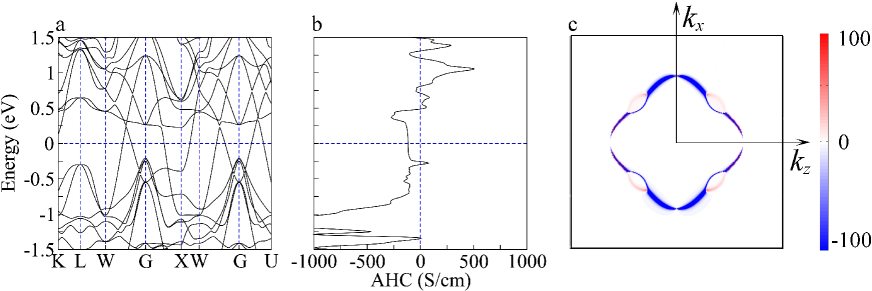
The gapless nodal line band structure contains non zero Berry curvatures around it, however, they are helically distributed in the mirror plane and the total flux is zero. Hence the gapless nodal line in plane does not contribute to the intrinsic anomalous Hall conductivity. On the other hand, the nodal lines in and planes are broken by the magnetization, which also force the Berry curvature to orient along the direction of magnetization. Taking plane as an example, as presented in Figure 1c, the points around the broken nodal lines are dominated by negative components of the Berry curvature, and directly contribute to the negative anomalous Hall effect, which shares the same mechanism of strong spin Hall effect in nodal line materials Sun30 ; Sun31 . Since the nodal lines in mirror planes have strong energy dispersion Wang21 ; Chang29 , only part of the nodal lines contribute to the anomalous Hall conductivity at fixed Fermi level. The intrinsic anomalous Hall conductivity almost keeps constant at about 100 S/cm in the range of -0.25 to 0.25 eV, which is just inside the energy window of the dispersion of the nodal lines, see Figure 1a and b. Therefore, the anomalous Hall conductivity in Co2TiSn mainly originates from the magnetization induced gaps by breaking the nodal line band structure.
III.2 Structural properties of the thin films
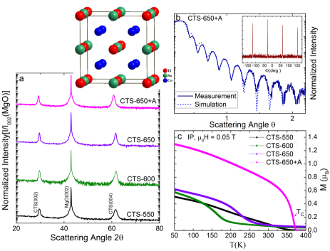
In this and the following sections we focus on the experimental findings, starting with the crystal structure of the epitaxial Co2TiSn films grown under different conditions as mentioned in the experimental section. Figure 2a depicts XRD pattern for various Co2TiSn films. All films exhibit (002) and (004) peaks of the cubic Heusler structure along with (002) peak of the MgO substrate. The crystal structure of Heusler compounds is presented in the inset of Figure 2a. In this structure, Co , Ti and Sn atoms occupy the Wyckoff positions 8c, 4b, and 4a, respectively.
The cubic lattice parameter CTS-550 is found to be Å. The shift of the XRD peaks towards lower value points on an increase of the lattice parameter with higher growth temperatures. The lattice parameter for CTS-650+A is finally 6.1 Å. The epitaxial relationship of the films with substrate is found to be [100] Co2TiSn [110] MgO. X-ray reflectivity (XRR) was measured to determine the thickness and surface smoothness of the film. The XRR measurement for CTS-650+A is shown in Figure 2b. The clear oscillation of fringes suggests that the surface of this film is smooth and homogeneous. Upon fitting the XRR curve, the thickness and roughness are estimated to be 22 nm and 0.3 nm, respectively. The -scan performed along the (111) plane displays four sharp maxima at equal intervals, exemplifying four fold symmetry of the present cubic structure (inset in Figure 2b).
From EDX analysis the composition of CoTiSn films is confirmed to be 2:1:1 within error of 5%.
III.3 Hard x-ray photoelectron spectroscopy
Besides by XRD and XRR measurements, the films were further investigated with respect to their quality by Hard x-ray photoelectron spectroscopy. HAXPES is a powerful technique that is utilized to understand the detailed electronic structure of all type of materials Zegenhagen34 . It helps to investigate the bulk electronic structure as was explained in detail for Heusler compounds in References [Fecher35, ; Ouardi36, ]. The high kinetic energy electrons exhibit a large probing depth inside the material and provide with bulk properties that are free of surface effects. In particular, the details of the valence band density of states are probed due to the integration over a large volume in momentum space at high kinetic energies. Therefore, the HAXPES valence band spectrum (see Figure 3b) has been measured for the well-ordered CTS-650+A and is compared to the calculated density of states as shown in Figure 3a. In the valence band spectrum the high intensity at -9.3 eV arises from the contribution of electrons that are mainly localized close to the Sn atoms according to the calculations. On the other hand, a minimum appears at about -7.3 eV that reflects the hybridization gap in the density of states and is typical for Heusler compounds. In the upper part of the spectrum, four maxima emerge at -5.8, -3.5, -2.0, and -0.4 eV binding energies. The feature at -3.5 eV arises from the hybridization of Co states with Sn states. Closer to the Fermi energy, the spectra are dominated by states localized mainly at the Co atoms. The valence band spectrum thus reflects the most dominant features of the calculated density of states, accounting for matrix elements that redistribute the intensities compared to the densities.
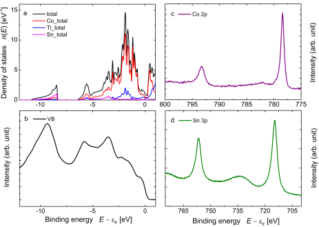
Core level spectra are used to explain the cleanness of the compound and with restrictions its electronic state, chemical order, and composition. The Co core level spectrum (Figure 3c) exhibits a distinct spin-orbit splitting of 14.9 eV. A similar size of the spin-orbit splitting (14.95 eV) was also reported for polycrystalline samples Barth14 . No oxide related features at 2-3 eV higher binding energy compared to the Co main peak are detected. The Sn core level spectra exhibit a large spin orbit splitting of about 42 eV (Figure 3d) together with pronounced side maxima. These broad transitions emerge not as primary excitations but as energy loss structures from secondary band–band or plasmon excitations. The later result from the free electron type behavior of the electrons localized mostly close to Sn, as mentioned above. Again, no oxygen or other impurity related features are detected. This indicates, together with the Co spectra, the cleanness of the sample. In all cases, no significant chemical shifts of core level binding energies are found in Co2TiSn. These signify the metallic character of the compound. All observed features are in qualitative agreement with the previous HAXPES measurement on polycrystalline bulk samples Barth14 , reflecting the high quality of the thin films.
III.4 Magnetic and electrical properties
This section reports on the magnetic properties and Hall effect measurements of the epitaxially grown Co2TiSn thin films. Figure 2c shows the temperature dependent magnetization curves that are measured in field cooled mode in presence of an in-plane field of 0.05 T. For CTS-550, the magnetic transition is quite broad in nature without a well-defined Curie temperature (). With increasing growth temperatures CTS-600 and CTS-650 exhibit a well-defined of about 160 K and 225 K, respectively. However, the non-zero magnetization above for these films indicates the presence of some disorder. We found by annealing of CTS-650 that a very sharp of K is obtained for the CTS-650+A film. For bulk Co2TiSn, a of 355 K has been reported by Barth et al. Barth14 . It should be mentioned here that the trend of in the observed films is an important factor to determine the degree of order / disorder in the system. The observation of undefined or low in CTS-550, CTS-600, and CTS-650 suggests the presence of large chemical disorder. For instance, Meinert et al. Meinert13 have reported a considerable decrease in atomic disorder with increasing deposition temperature. The presence of type Co-Ti antisite disorder, as found by NMR and Mößbauer measurements, has also been reported for bulk Kandpal5 . Therefore, disorder plays an important role in the present system. It can be reduced considerably using higher substrate temperatures during growth.
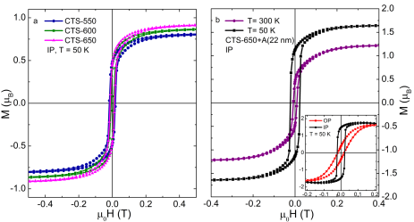
In-plane magnetic hysteresis loops for different Co2TiSn films measured at 50 K are presented in Figure 4a. The saturation magnetic moment per formula unit increases with increasing growth temperature from 0.8 for CTS-550 to 0.9 for the CTS-650. For CTS-650+A the saturated moment further increases to 1.6 at 50 K and 1.2 at 300 K (Figure 4b). The presence of an in-plane easy axis is confirmed by the measurement of out of plane (OP) loops that exhibit a hard-axis type hysteresis (Figure 4b) in the present film. The finding of a larger magnetic moment and higher for CTS-650+A suggest that the improvement of the chemical order by annealing helps to enhance the magnetic properties.
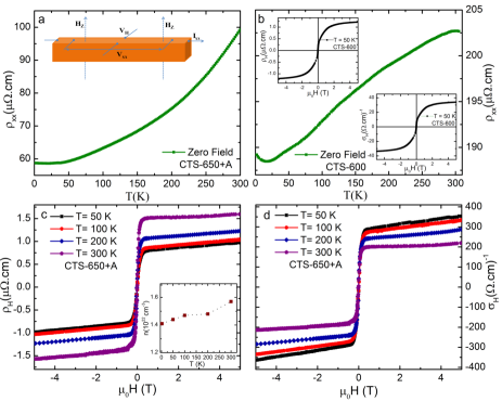
To characterize the AHE in the present thin films, we have carried out detailed electrical transport measurements. A schematic diagram of the present measurements is presented in the inset of Figure 5a. In the given configuration, the current () is applied along [100], the magnetic field () is applied along [001] and the lateral Hall voltage () is measured along [010]. As shown in Figure 5a, the temperature dependence of the linear resistivity () measured at zero field exhibits a metallic characteristic. values of 58 cm and 100 cm are obtained at temperatures of 2 K and 300 K, respectively. Although CTS-600 displays a metallic behavior in the resistivity measurement, the magnitude of resistivity is fairly higher than that of CTS-650+A. The higher residual resistivity of CTS-600 clearly indicates the presence of higher disorder, as discussed earlier. The residual resistivity ratio is calculated from the resistivities at low (2 K) and high (300 K) temperatures: RRR = (300 K)/(2 K). For CTS-650+A, we find a RRR value of 1.7, whereas, it is 1.07 for CTS-600. The lower RRR value implies higher impurity scattering due to larger disordered in CTS-600.
The Hall resistivity is obtained by measuring the transverse Hall voltage as shown in the schematic diagram in the inset of Figure 5a. In a ferromagnet, is usually written as,
| (2) |
where and are the normal and anomalous Hall coefficients, is the vacuum permeability. The first term is the ordinary Hall resistivity that arises from the Lorentz force and the second term illustrates the anomalous Hall contribution that originates from the intrinsic magnetisation. Figure 5c presents versus applied field for the film CTS-650+A. initially increases with field before tending towards saturation. A weak linear increase in at higher field emerges from the contribution of the ordinary Hall effect. Contrary to the magnetic behavior, where higher magnetization is observed at lower temperature, of 1 cm is obtained at 50 K and increases to 1.5 cm at 300 K. The Hall conductivity () has been calculated using the formula
| (3) |
The field dependence of the Hall conductivity is plotted in Figure 5d. increases rapidly under a relatively small field due to the anomalous contribution. This anomalous contribution has values of 284 S/cm and 180 S/cm at 50 K and 300 K, respectively. In contrary, CTS-600 shows a Hall conductivity of about 35 S/cm at 50 K (inset of Figure 5b). The Hall coefficient for CTS-650+A is obtained from the slope of versus . It is observed that the Hall coefficient is positive for all temperatures, which suggests that the charge carriers are of hole type, or correspondingly, the electrons have a negative effective mass. The carrier concentration is calculated from the Hall constant , where is the electron charge. The carrier concentration is calculated to be cm-3 at 300 K, which corresponds to a metallic kind of behavior.
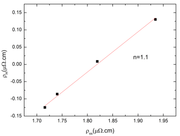
Further, we discuss the physical origin of the anomalous Hall effect in CTS- 650+A. From the Berry curvature calculations, it is found that a anomalous Hall conductivity of 100 S/cm is attained in Co2TiSn, whereas, the measurement gives an anomalous Hall conductivity of S/cm. In order to understand the difference, it is necessary to find out whether there is any contribution from any extrinsic mechanisms, such as, skew scattering or side jump effect Smith32 ; Berger33 . An easier approach to explain this mechanism is by verifying the scaling law between and by the formula . Here, equal to 1 and 2 correspond to the skew scattering and side jump mechanisms, respectively Nagaosa17 . In Figure 6, the Hall resistivity is plotted as a function of the linear resistivity in log10 form. The data are fitted well by a linear dependence with a slope of . This suggests that the extrinsic effect, that is the skew scattering mechanism, may dominate in this case. It is important to mention here that a linear conductivity of S/cm is observed in the given film. This value falls into the category of a moderate conductivity regime, where it is considered that the anomalous Hall effect mainly arises from the intrinsic mechanism Nagaosa17 . However from the current analysis presented in Figure 6, it seems that skew scattering also contributes to the anomalous Hall effect in the investigated film.
IV SUMMARY
In summary, Berry curvature calculations have been performed for Co2TiSn and an intrinsic anomalous Hall conductivity of 100 S/cm is calculated. The anomalous Hall conductivity originates from slightly gapped nodal lines due to a symmetry reduction induced by the magnetization. From the present analysis, it is also found that Weyl points exist few hundreds meV above the Fermi energy. The position of the Weyl nodes may be manipulated to appear at the Fermi energy by doping Co2TiSn to increase the valence electron concentration. Moreover, the valence band HAXPES spectra measured for the well-ordered Co2TiSn film suggests that the electronic structure in this film is in agreement to the calculated density of states. Experimentally, the well-ordered film exhibits an anomalous Hall conductivity of 284 S/cm and 180 S/cm at 50 K and 300 K, respectively. These values are in good agreement with the theoretical prediction. The slightly larger value of the measured anomalous Hall conductivity is attributed to the skew scattering mechanism. The present work emphasizes the potential of Co2TiSn for future spintronics applications.
V ACKNOWLEDGEMENT
The authors thank J. Kübler for useful theoretical discussions, C. Shekhar for measuring transport properties, and E. Ikenaga for experimental support during the HAXPES measurements. The synchrotron radiation HAXPES experiments were performed at BL47XU of Spring-8 with approval of JASRI (Proposal No.2016B1086). This work was financially supported by the Max Planck Society and by the ERC Advanced Grant (291472) ”Idea Heusler”.
References
- (1) S. S. P. Parkin, X. Jiang, C. Kaiser, A. Panchula, K. Roche, and M. Samant, Proc. IEEE 91, 661-680 (2003).
- (2) F. Pulizzi, Nature Mater. 11, 367 (2012).
- (3) C. Felser and G. H. Fecher (Eds.). Spintronics; From Materials to devices. Springer Verlag, Dordrecht, Heidelberg, New York, London, 2013.
- (4) T. Graf, C. Felser, and S. S. P. Parkin, Prog. Solid State Chem. 39, 1 (2011).
- (5) J. Kübler, G. H. Fecher, and C. Felser, Phys. Rev. B. 76, 024414(2007).
- (6) H. C. Kandpal, G. H. Fecher, and C. Felser, J. Phys. D: Appl. Phys. 40, 1507(2007).
- (7) R. Sahoo, L. Wollmann, S. Selle, T. Höche, B. Ernst, A. Kalache, C. Shekhar, N. Kumar, S. Chadov, C. Felser, S. S. P. Parkin, and A. K. Nayak, Adv. Mater. 28, 8499 (2016).
- (8) J. Kübler, A. R. Williams, and C. B. Sommers, Phys. Rev. B. 28, 1745 (1983).
- (9) I. Galanakis, P. H. Dederichs, and N. Papanikolaou, Phys. Rev. B. 66, 174429 (2002).
- (10) J. Sato, M. Oogane, H. Naganuma, and Y. Ando, Appl. Phys. Express 4, 113005 (2011).
- (11) N. Tezuka, N. Ikeda, F. Mitsuhashi, and S. Sugimoto, Appl. Phys. Lett. 94, 162504 (2009).
- (12) H. Liu, Y. Honda, T. Taira, K. Matsuda, M. Arita, T. Uemura, and M. Yamamotoa, Appl. Phys. Lett. 101, 132418 (2012).
- (13) M. Meinert, J. Schmalhorst, H. Wulfmeier, G. Reiss, E. Arenholz, T. Graf, and C. Felser, Phys. Rev. B. 83, 064412 (2011).
- (14) J. Barth, G. H. Fecher, B. Balke, S. Ouardi, T. Graf, C. Felser, A. Shkabko, A. Weidenkaff, P. Klaer, H. J. Elmers et al. Phys. Rev. B. 81, 064404 (2010).
- (15) H. C. Kandpal, V. Ksenofontov, M. Wojcik, R. Seshadri, and C. Felser, J. Phys. D: Appl. Phys. 40, 1587 (2007).
- (16) J. Barth, G. H. Fecher, B. Balke, T. Graf, A. Shkabko, A. Weidenkaff, P. Klaer, M. Kallmayer, H. J. Elmers, H. Yoshikawa, S. Ueda, K. Kobayashi, and C. Felser, Phil. Trans. R. Soc. A. 369, 3588 (2011).
- (17) N. Nagaosa, J. Sinova, S. Onoda, A. H. MacDonald, and N. P. Ong, Rev. Mod. Phys. 82, 1539 (2010).
- (18) A. K. Nayak, J. E. Fischer, Y. Sun, B. Yan, J. Karel, A. C. Komarek, C. Shekhar, N. Kumar, W. Schnelle, J. Kübler, C. Felser, and S. S. P. Parkin, Sci. Adv. 2, e1501870 (2016).
- (19) S. Nakatsuji, N. Kiyohara, and T. Higo, Nature 527, 212-215 (2015).
- (20) S. Ouardi, G. H. Fecher, and C. Felser, J. Electr. Spectr. Rel. Phenom. 190, 249 (2013).
- (21) G. H. Fecher and C. Felser, Hard X-Ray Photoelectron Spectroscopy of New Materials for Spintronics, chapter 11, page 243. Springer Verlag, Dordrecht, Heidelberg, New York, London, 2013.
- (22) J. Kübler and C. Felser, Europhys. Lett. 114, 47005 (2016).
- (23) Z. Wang, M. G. Vergniory, S. Kushwaha, M. Hirschberger, E. V. Chulkov, A. Ernst, N. P. Ong, R. J. Cava, and B. A. Bernevig, Phys. Rev. Lett. 117, 236401 (2016).
- (24) J. Kübler and C. Felser, Phys. Rev. B. 85, 012405 (2012).
- (25) G. Kresse and J. Furthmüller, Phys. Rev. B 54, 11169 (1996).
- (26) G. Kresse and J. Furthmüller, Comput. Mater. Sci. 6, 15 (1996).
- (27) J. P. Perdew, K. Burke, and M. Ernzerhof, Phys. Rev. Lett. 77, 3865 (1996).
- (28) N. Marzari and D. Vanderbilt, Phys. Rev. B 56, 12847 (1997).
- (29) I. Souza, N. Marzari ,and D. Vanderbilt, Phys. Rev. B 65, 035109 (2001).
- (30) A. A. Mostofi, J. R. Yates, Y. S. Lee, I. Souza, D. Vanderbilt, and N. Marzari, Comput. Phys. Commun. 178, 685 (2008).
- (31) G. Chang, S. Y. Xu, H. Zheng, B. Singh, C. H. Hsu, I. Belopolski, D. S. Sanchez, G. Bian, N. Alidoust, H. Lin, and M. Z. Hasan, Scientific Reports. 6, 38839 (2016).
- (32) Y. Sun, Y. Zhang, C. Felser, and B. Yan, Phy. Rev. Lett. 117, 146403 (2016).
- (33) Y. Sun, Y. Zhang, C. X. Liu, C. Felser, and B. Yan, arXiv:1701.09089 (2017).
- (34) Detailed reviews of the method are found in Proceedings of the Workshop on Hard X-Ray Photoelectron Spectroscopy, J. Zegenhagen and C. Kunz, [Nucl. Instrum. Methods Phys. Res., Sect. A 547, No. 1 (2005).
- (35) G. H. Fecher, B. Balke, A. Gloskowskii, S. Ouardi, C. Felser, T. Ishikawa, M. Yamamoto, Y. Yamashita, H. Yoshikawa, S. Ueda, and K. Kobayashi, Appl. Phys. Lett. 92, 193513 (2008).
- (36) S. Ouardi, G. H. Fecher, X. Kozina, G. Stryganyuk, B. Balke, C. Felser, E. Ikenaga, T. Sugiyama, N. Kawamura, M. Suzuki, and K. Kobayashi, Phys. Rev. Lett. 107, 036402 (2011).
- (37) J. Smith, Physica. 24, 39 (1958).
- (38) L. Berger, Phys. Rev. B. 2, 4559 (1970).