Structural origin of the midgap electronic states and the Urbach tail in pnictogen-chalcogenide glasses
Abstract
We determine the electronic density of states for computationally-generated bulk samples of amorphous chalcogenide alloys AsxSe100-x. The samples were generated using a structure-building algorithm reported recently by us (J. Chem. Phys. 147, 114505). Several key features of the calculated density of states are in good agreement with experiment: The trend of the mobility gap with arsenic content is reproduced. The sample-to-sample variation in the energies of states near the mobility gap is quantitatively consistent with the width of the Urbach tail in the optical edge observed in experiment. Most importantly, our samples consistently exhibit very deep-lying midgap electronic states that are delocalized significantly more than what would be expected for a deep impurity or defect state; the delocalization is highly anisotropic. These properties are consistent with those of the topological midgap electronic states that have been proposed by Zhugayevych and Lubchenko as an explanation for several puzzling opto-electronic anomalies observed in the chalcogenides, including light-induced midgap absorption and ESR signal, and anomalous photoluminescence. In a complement to the traditional view of the Urbach states as a generic consequence of disorder in atomic positions, the present results suggest these states can be also thought of as intimate pairs of topological midgap states that cannot recombine because of disorder. Finally, samples with an odd number of electrons exhibit neutral, spin midgap states as well as polaron-like configurations that consist of a charge carrier bound to an intimate pair of midgap states; the polaron’s identity—electron or hole—depends on the preparation protocol of the sample.
I Introduction
In contrast with their periodic counterparts, amorphous materials are expressly non-Bloch solids. Despite this complication, many amorphous semiconductors purvey electricity similarly to the corresponding crystals. Indeed, from the viewpoint of the wave-packet representing a charge carrier, the pertinent molecular orbitals are virtually indistinguishable from true, infinitely-extended Bloch states as long as the mean-free path of the carrier is less than the extent of the orbitals. Thus one may still speak of mobility bands even in the absence of strict periodicity. Anderson (1958); Mott (1982); Cohen et al. (1969); Mott (1990) In addition, many families of crystalline and amorphous compounds alike are expected to exhibit conduction by strongly localized, “polaronic” charge carriers, when the electron-lattice interaction is sufficiently strong. Emin (1983a, b) These ideas are graphically summarized in Fig. 1.
Because of the electron-lattice coupling, on the one hand, and the constant thermal motion of atoms, on the other hand, the optical edge in semiconductors is not sharp whether the solid is periodic or not: This is because optical excitations are much faster than nuclear motions implying that, effectively, electrons are always subject to an aperiodic Born-Oppenheimer potential. The effective band edge turns out to be nearly exponential and is often called the Urbach tail. Urbach (1953); Toyozawa (1961); Dow and Redfield (1972); Mahan (1966); Kostadinov (1977); Brezin and Parisi (1980); Cardy (1978); John et al. (1986); Zittartz and Langer (1966); Economou et al. (1970) Now in amorphous materials, there is no underlying long-range order even with regard to vibrationally-averaged atomic positions. Thus the disorder in the atomic locations is partially frozen-in. Because such frozen glasses can be very far away from equilibrium, the distribution of the energies of the localized states is generally decoupled from the ambient temperature (and pressure) and, furthermore, depends on the preparation protocol of the sample. Lubchenko and Wolynes (2004, 2018) Appropriately, exponential tails of localized states generically emerge in models with quenched disorder, within the venerable Anderson-Mott framework of electron localization in disordered media. Anderson (1958); Mott (1982); Cohen et al. (1969); Mott (1990) Those approaches assume generic forms for the random one-electron potential. Non-withstanding the seemingly general character of the resulting predictions, such generic approaches are not fully constructive in that the random potential they postulate may not be consistent with the actual molecular field in a stable structure. In a constructive treatment, such a potential must arise self-consistently.
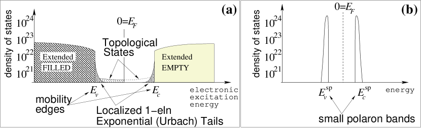
An additional, seemingly separate set of electronic excitations have been observed in glassy chalcogenides. These excitations are apparently activated by exposing the sample to macroscopic quantities of photons at supra-gap frequencies. The excitations reveal themselves as optical absorption at midgap frequencies and concomitant emergence of ESR signal, Biegelsen and Street (1980); Hautala et al. (1988); Shimakawa et al. (1995); Bishop et al. (1977); Mollot et al. (1980) and anomalous photo-luminescence. Tada and Ninomiya (1989a, b, c) The concentration of these seemingly intrinsic defect-like states is estimated at cm-3, Biegelsen and Street (1980) i.e. one per several hundred atoms. This is much greater, for instance, than the typical amount of dopants in crystalline semiconductors, and leads to a very efficient pinning of the Fermi energy. At the same time, the glassy chalcogenides are not amenable to conventional doping. Kolomiets (1981); Mott (1993)
According to an early microscopic proposal, due to Anderson Anderson (1975, 1976), such behavior would be observed, if electrons exhibited effective mutual attraction when occupying a localized orbital so that per electron, the energy of a filled orbital is lower than that of a singly-occupied orbital. (The subset of such special orbitals would be relatively small.) The effective attraction could stem, for instance, from lattice polarization and would amount to an effective negative Hubbard . Shortly thereafter, Street and Mott Street and Mott (1975) argued that given a certain, large number of dangling bonds, nearby pairs of such bonds will be unstable toward the formation of intimate pairs of malcoordinated configurations, one negatively and one positively charged. (The dangling bonds themselves are electrically neutral.) Kastner et al., Kastner et al. (1976) put forth specific microscopic proposals as to the specific atomic motifs that could host such valence alternation pairs (VAP). In addition, Vanderbilt and Joannopoulos Vanderbilt and Joannopoulos (1981) proposed candidate malcoordinated configurations that do not have to come in pairs but are standalone. In these approaches, the defect states are viewed as essentially defects in an otherwise perfect crystalline lattice. In a more recent effort, Li and Drabold Li and Drabold (2000) have produced candidate defected configurations by modeling light-induced formation of relatively malcoordinated motifs in computer generated aperiodic samples.
In a distinct approach, Zhugayevych and Lubchenko Zhugayevych and Lubchenko (2010a, b) (ZL) have argued that chalcogenide glasses must host special midgap electronic states that would be intrinsic to any glass exhibiting spatially-inhomogeneous bond saturation. (In the case of the chalcogenides, the bond strength varies between that of a canonical single bond and a formally closed-shell,Pyykkö (1997) secondary bond.) These midgap states are tied to relatively strained regions that are intimately related to transition-state configurations for activated transport in an equilibrated glassy liquid, as well as for aging in a frozen glass. Lubchenko and Wolynes (2004, 2018) The strained configurations can be thought of as domain walls separating distinct aperiodic minima of the free energy; they must be present in thermodynamic quantities. The equilibrium concentration of the domain walls just above the glass transition has been estimated at cm-3, using the random first order transition (RFOT) theory; Xia and Wolynes (2000); Lubchenko and Wolynes (2001, 2007); Lubchenko (2015) this figure matches well the apparent quantity of the light-activated midgap states. Since the structure of the liquid becomes largely arrested below the glass transition—apart from some aging Lubchenko and Wolynes (2004) and a minor decrease in the vibrational amplitude—the concentration of the strained regions remains steady upon cooling the glass. When expressed in terms of the size of a rigid molecular unit, this concentration is nearly universal for two reasons: On the one hand, it depends only logarithmically on the time scale of the glass transition. On the other hand, the dependence of the concentration of the midgap states on the material constants is only through the so called Lindemann ratio. This ratio is defined as the relative vibrational displacement near the onset of activated transport and happens to be a nearly universal quantity. Lubchenko (2006); Rabochiy and Lubchenko (2012) Thus doping the material may shift the glass transition temperature, but will not significantly affect the concentration of the intrinsic midgap states. The robustness of the ZL midgap states has a topological aspect, too: They can be thought of as stemming from an extra or missing bond on an atom while the malcoordination cannot be removed by elastically deforming the lattice. At most, lattice relaxation results in the malcoordination being “smeared” over a substantial region. This smearing is accompanied by further delocalization of an already surprisingly extended wave-function of the midgap electronic state. The overall extent of the wavefunction can be in excess of a dozen lattice spacings, which is much greater than what one would expect for a very deep impurity state.
Analogous in many ways to the solitonic midgap states in trans-polyacetylene, Heeger et al. (1988) the midgap states can be thought of as composed of an equal measure of the states from the valence and conduction band. As a result, their energy is efficiently pinned near the center of the mobility gap, if the states are singly-occupied and, thus, neutral. Such neutral states absorb light at sub-gap frequencies. However in a pristine sample, the midgap states are occupied or vacant—corresponding with being negatively and positively charged respectively—and thus stabilized owing to lattice polarization. Zhugayevych and Lubchenko (2010a, b) Because of the lattice distortion, charged midgap states absorb at supra-gap frequencies. Anderson (1975, 1976); Zhugayevych and Lubchenko (2010b) These notions underlie the light-induced emergence of ESR signal and midgap absorption: Zhugayevych and Lubchenko (2010b) Supra-gap irradiation excites electrons from filled midgap states into the conduction band; in addition filled midgap states can capture the oppositely charged free carriers produced by the irradiation. As a result, the midgap states become electrically neutral and begin to absorb light at sub-gap frequencies. Thus in the ZL scenario, the specific atomic motifs giving rise to the midgap states are not light generated defects; instead they are intrinsically present in the structure. Light only serves to make the defects ESR- and optically-active—at sub-gap frequencies—by making them half-filled.
Some of these aspects of the topological midgap states are reminiscent of the negative- model of Anderson Anderson (1975, 1976) and subsequent ad hoc defect-based models mentioned above.Kastner et al. (1976); Street and Mott (1975); Vanderbilt and Joannopoulos (1980) In fact, some of those defect states can be viewed as an ultra-local limit of the ZL theory. Zhugayevych and Lubchenko (2010b) In those earlier developments, however, the concentration of the defects is tied to the number of specific molecular motifs whose quantity would seem to depend on the stoichiometry. Nor is it clear whether such defected configurations could combine to form a stable lattice. In the ZL treatment, the concentration is predicted to be inherently at roughly one defect per several hundred atoms, irrespective of the precise stoichiometry. The defect concentration is determined by an interplay between the enthalpic cost of forming the domain walls, on the one hand, and their entropic advantage, on the other hand. This entropic advantage can be ultimately be traced to the excess liquid entropy of the supercooled liquid relative to the corresponding crystal.
ZL Zhugayevych and Lubchenko (2010b) have also proposed specific malcoordinated motifs underlying the midgap states. The motifs consist of relatively extended -bonded chains connecting an odd number of orbitals, at half filling. The presence of such motifs is expected on a systematic basis, insofar as one may regard the chalcogenides as distorted versions of relatively symmetric, parent structures defined on the simple cubic lattice. Zhugayevych and Lubchenko (2010c) Parent structures defined on the simple cubic lattice have been indeed obtained for all known lattice types found in stoichiometric crystalline compounds of the type Pn2Ch3 (Pn P, As, Sb, Bi, Ch S, Se, Te), Golden (2016) and are themselves periodic of course. ZL anticipated that aperiodic parent structures, upon deformation, would give rise to bona fide glassy structures. Thus the aperiodicity and the sporadic malcoordination of the lattice would arise self-consistently. ZL Zhugayevych and Lubchenko (2010b) have generated standalone, molecular malcoordinated motifs, which were properly passivated to emulate proper coordination appropriate for a 3D solid. It was argued that the interaction of defect-bearing chains with the surrounding solid amounts to a renormalization of the on-site energies and electron hopping elements along the chain but would not change the physics qualitatively—a notion that will be revised in this article. No attempt was made to generate a bulk three-dimensional structure that would host such motifs while obeying local chemistry throughout.
Here we report what we believe is the first realization of the topological midgap states in bulk samples. The samples were generated using a structure-building algorithm reported earlier by us. Lukyanov and Lubchenko (2017) In this algorithm, one first generates so called parent aperiodic structures that exhibit octahedral coordination, locally. A subset of the lattice sites in the parent structure form a random-close packed structure, Parisi and Zamponi (2010) thus ensuring that within a certain range of wavelengths, the structures are at what is believed to be the highest achievable density for aperiodic solids. These parent structures are subsequently optimized using quantum-chemical force fields while coordination becomes distorted-octahedral. Zhugayevych and Lubchenko (2010c) Thus the sample is not generated by quenching a melt that had been equilibrated at some high temperature. In principle, such quenched samples should approximate real materials subject only to the accuracy of the effective inter-atomic force fields and, possibly, finite-size effects. In practice, however, the dynamical range of molecular dynamics simulations is very limited even for relatively simple model liquids let alone the chalcogenides, where the effective force fields between the atoms must be determined using computationally expensive, quantum-chemical approximations. As a result, one can equilibrate a chalcogenide melt only at temperatures much exceeding the laboratory glass transition. The resulting samples are thus hyper-quenched while their structure exhibits exaggerated effects of mixing entropy in the form of excess homo-nuclear contacts even in the stoichiometric compound As40Se60, in contrast with observation. Deschamps et al. (2015)
The parent structures generated in Ref. Lukyanov and Lubchenko (2017) do not contain homonuclear contacts by construction, nor do such defects seem to appear in significant quantities following the geometric optimization, at least in the stoichiometric compound As40Se60. We have argued Lukyanov and Lubchenko (2017) this circumstance explains why the resulting amorphous samples consistently exhibit the first sharp diffraction peak (FSDP) in the structure factor, including its trends with pressure and arsenic content. (The FSDP is the hallmark of the poorly understood medium-range-order Elliott (1991); Salmon et al. (2005) in inorganic glasses.) In contrast, samples generated using first principles molecular dynamics often fail to exhibit the FSDP. Bauchy et al. (2014)
Likewise, the electronic density of states (DOS) for the presently generated samples exhibit properties expected of the amorphous chalcogenides. On the one hand, the gross part of the electronic spectrum does not vary significantly from sample to sample; this part of the DOS thus can be attributed to the mobility bands. On the other hand, the states near the band edges are found to fluctuate in energy substantially, as is expected for the localized Urbach-tail states. In fact, the magnitude of the fluctuation matches well the width of the Urbach tail observed in experiment. Perhaps more interestingly, samples generated according to the procedure from Ref. Lukyanov and Lubchenko (2017) do indeed exhibit very deep-lying midgap states that are close to the gap center, closer than could possibly take place for an Urbach-tail state.
Both the presence of the midgap states in the computed spectra and the value of the gap itself are found to depend rather sensitively on the detailed quantum-chemical approximation, consistent with earlier studies, Perdew and Levy (1983); Sham and Schlütter (1983) requiring the relatively higher-end, computationally expensive hybrid DFT to solve for the electronic spectrum. (Plain DFT seems to suffice for structure optimization.) Consistent with the general predictions by ZL, Zhugayevych and Lubchenko (2010a) the wavefunctions of a subset of the midgap states are elongated preferentially in one direction, in contrast with the extended states comprising the mobility bands, which are isotropic. In addition, here we argue that a somewhat distinct physical possibility can be realized in which the wave function consists of a few linear fragments emanating from the same spot in space; this possibility was overlooked by ZL. Some of the samples we have generated appear to exhibit this urchin-like shape. At least in one case, we were able to clearly identify a motif that can be thought of as a passivated odd-numbered chain that must necessarily host a topological midgap state. Such states correspond to ZL chains with closed ends. Now, the aforementioned deep midgap states were unforced in the sense that the structures contained an even number of electrons and were geometrically optimized so that there are no intentionally broken bonds in the sample. By way of contrast, we have also generated samples containing an odd number of electrons, thus forcing the system to have a dangling bond. Here we find the resulting “defect” is often very deep in the forbidden gap. This is in contrast with what would be expected for a generic impurity state. In some cases, the defect states are so deep inside the gap that they can be thought of as electrically-neutral entities, where the electron charge is largely compensated by lattice polarization. Yet in some cases, the configurations are more reminiscent of the polarons in conjugated polymers.Heeger et al. (1988); Brazovskii and Kirova (1981) Finally, we have established that the Urbach states turn out to be intermediate—both in terms of their shape and degree of localization—between the extended band states and the topological states thus suggesting the Urbach states and the topological states are intimately related.
The article is organized as follows: Section II discusses the salient features of the presently obtained spectra, the forbidden gap and the Urbach tail states. In Section III we first briefly survey pertinent general properties of the topological midgap states for isolated chains and then use model calculations to demonstrate that such midgap states are robust even if the defected chain are coupled to other chains. In Section IV, we quantitatively characterize the very deep midgap states obtained in the present study and argue that they are, in fact, the topological midgap states predicted earlier by ZL. Section V provides a brief summary.
II Salient features of the density of states: Mobility bands and the Urbach tail of localized states
We have generated disordered structures for the binary compound arsenic selenide AsxSe100-x for three distinct stoichiometries , and , with the help of the algorithm described in Ref. Lukyanov and Lubchenko, 2017. In this algorithm, we first generate a chemically-motivated aperiodic parent structure, in which a subset of atoms are placed at the vertices of a random close-packed (RCP) lattice, called the “primary lattice.” A complementary subset of atoms is then placed at the vertices of the so called “secondary lattice,” which is generated according to a detailed algorithm to maximize octahedrality in local bonding while maintaining desired stoichiometry. This detailed algorithm uses a threshold parameter , which prescribes the precise way in which we break up the interstitial space of the primary lattice into cavities. For instance, for very small values of , the cavities will be all tetrahedral, the tetrahedra determined using the Delaunay triangulation. For sufficiently large values of , on the other hand, some of these tetrahedra are merged into higher order polyhedra. These higher order polyhedra host the vertices of the secondary lattice. To minimize the number of homonuclear bonds, the primary and secondary lattice are populated by distinct species. Here we focus exclusively on the so called C-type structures, for which the primary lattice is made of halcogens (selenium in this case).
By varying the value of the parameter , one can effectively control the amount of vacancies in the parent structures. This amount is equal to the number of non-tetrahedral cavities in excess of the number of pnictogens (for C-type structures). For instance, is convenient for the stoichiometric compound As40Se60 because the number of vacancies that must be made is small yet not too small so that one can generate sufficiently distinct structures by randomly choosing the locations for the vacancies. In addition to , we have also generated samples with and for the As20Se80 and As50Se50 compounds, respectively. Five samples were generated for each value of , for each compound, except for As40Se60, where we have generated eleven. Finally, the parent structures are geometrically optimized using plane-wave DFT as implemented in the package VASP Kresse and Hafner (1993, 1994); Kresse and Furthmüller (1996a, b) in the Perdew-Wang Perdew et al. (1992, 1993) (PW91) generalized gradient approximation (GGA) for the exchange-correlation energy. Optimization was performed both at constant pressure and volume; the corresponding structures are labelled const- and const-, respectively. We note that optimization at constant pressure, which thus allows for unit cell optimization, produces much better results for the first sharp diffraction peak. Throughout the paper, the samples As20Se80, As40Se60, and As50Se50 contain a total of 250, 330, and 304 atoms, respectively.
While producing good structures—this we have tested for crystalline As2Se3 Lukyanov and Lubchenko (2017)—GGA-based methods are known to substantially underestimate the value of the band gap in semiconductors and insulators. Perdew and Levy (1983); Sham and Schlütter (1983) Thus to evaluate the electronic density of states, we use here a more accurate, but computationally costly hybrid functional B3LYP. The latter approximation does much better in reproducing experimental figures for the band gap than plain DFT and some hybrid functionals; see the Supplemental Information for more detail. In the rest of the article, we report spectra that were obtained using the hybrid functional B3LYP. We set the one-electron energy reference at the Fermi energy as reported by VASP.
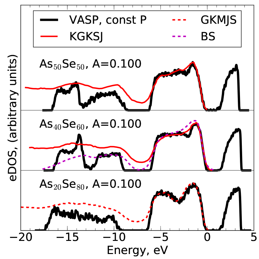
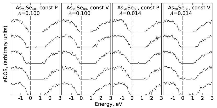
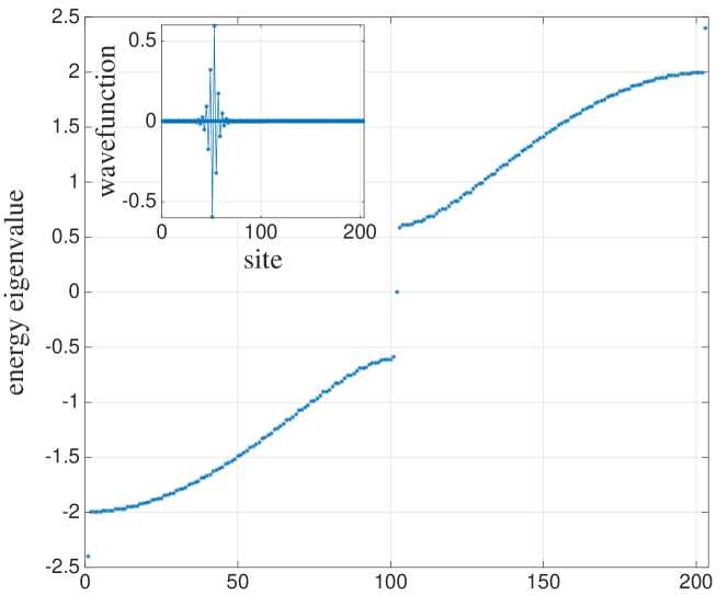
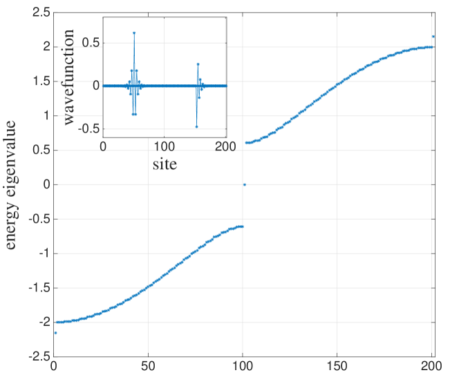
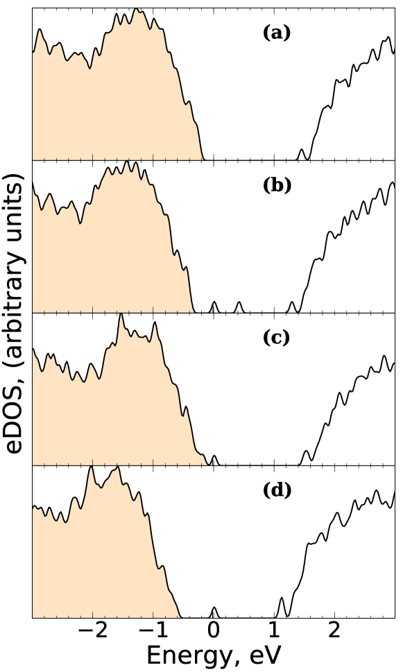
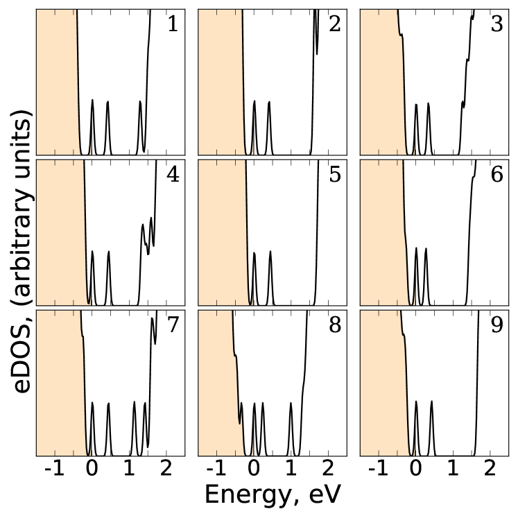
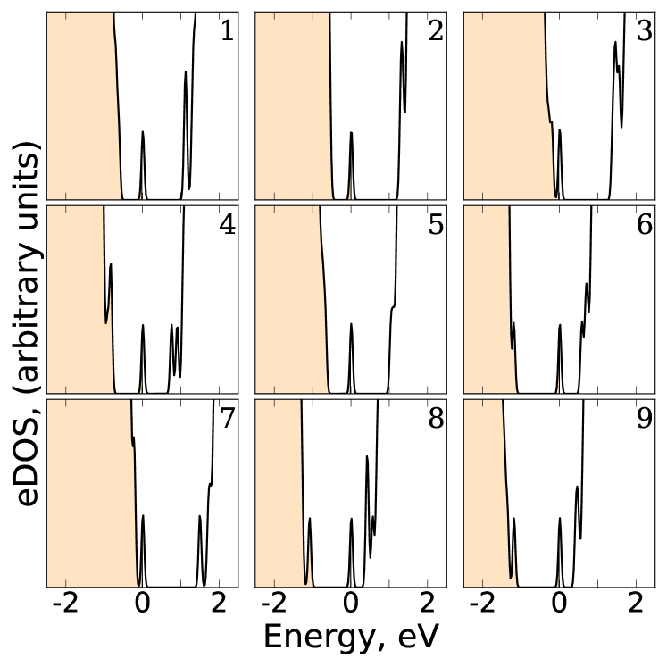
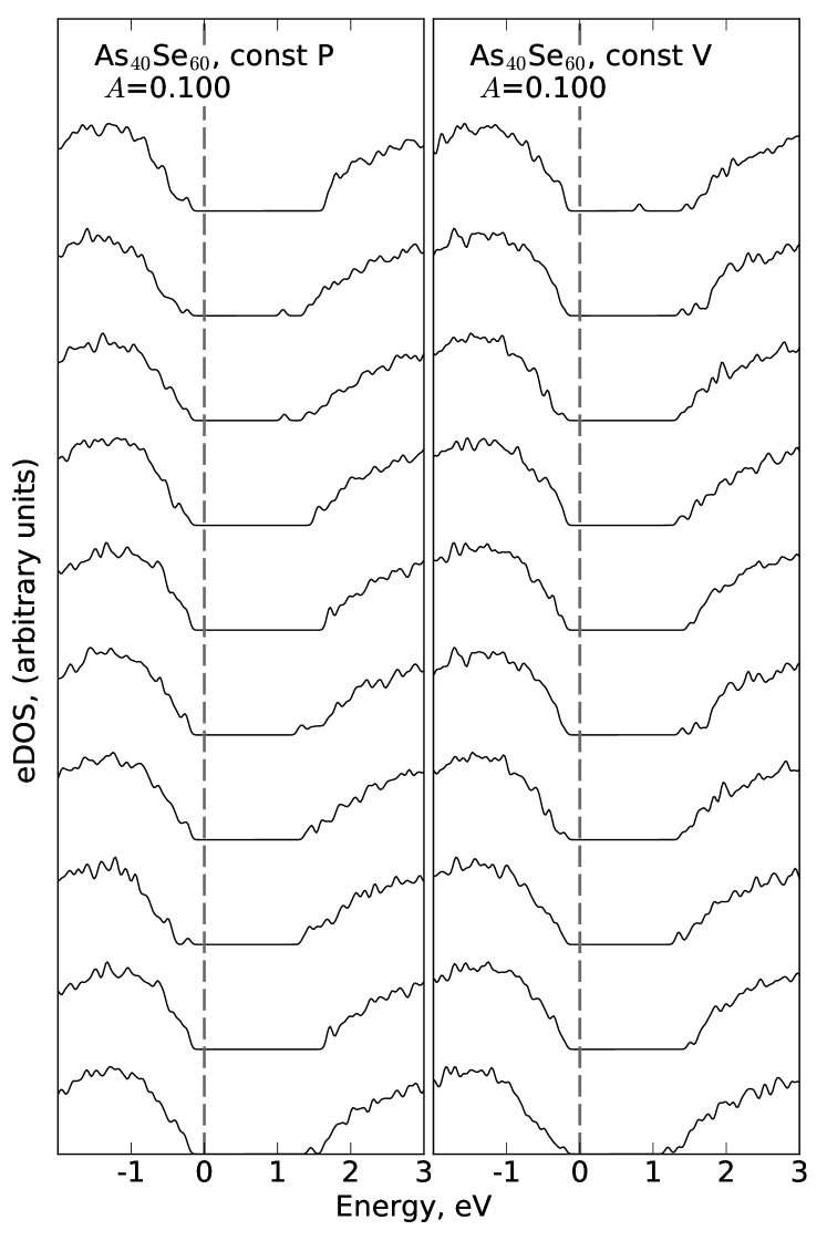
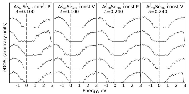
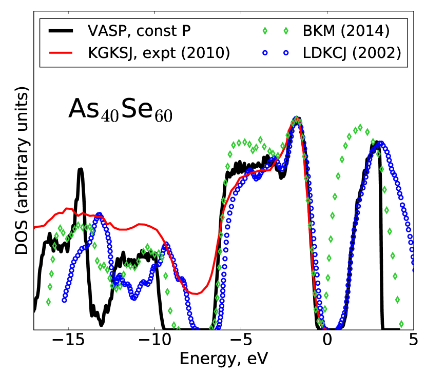
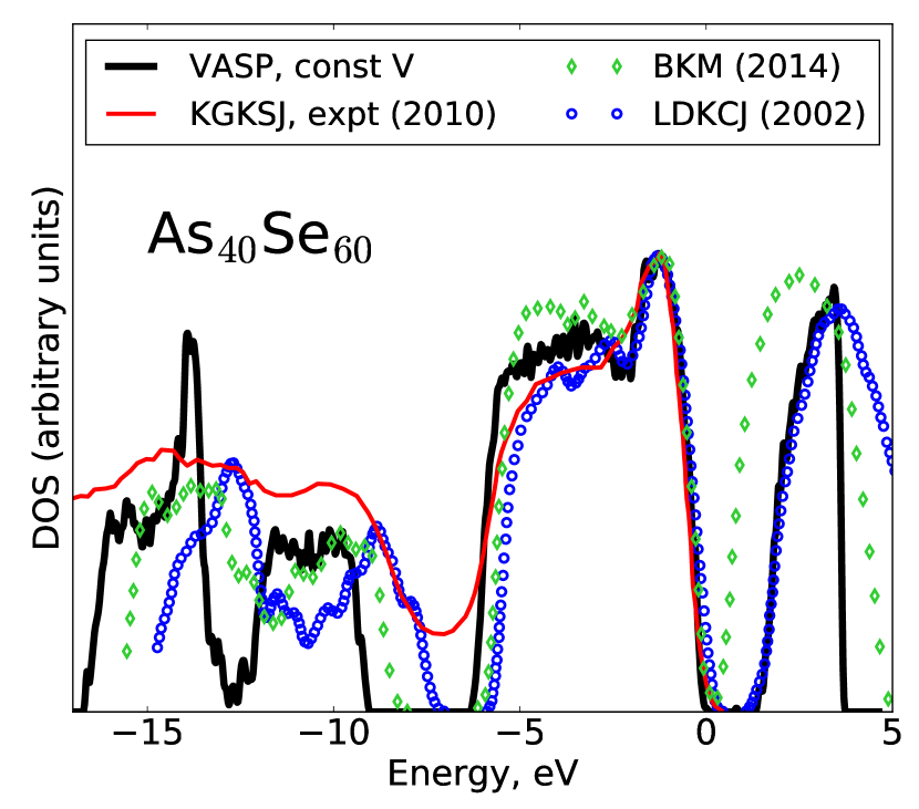
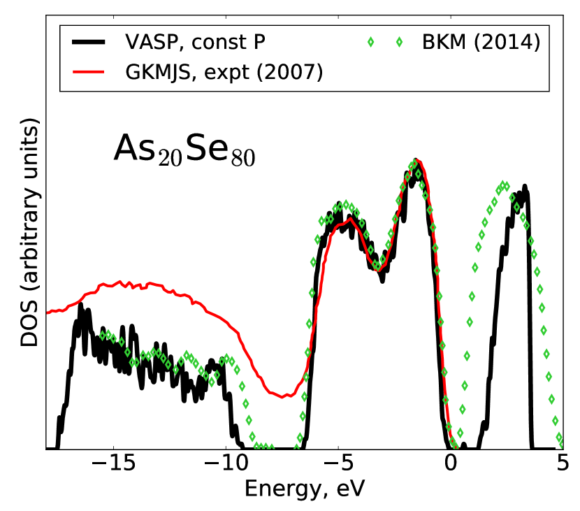
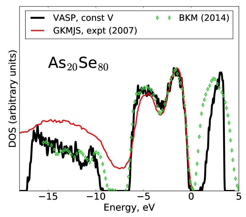
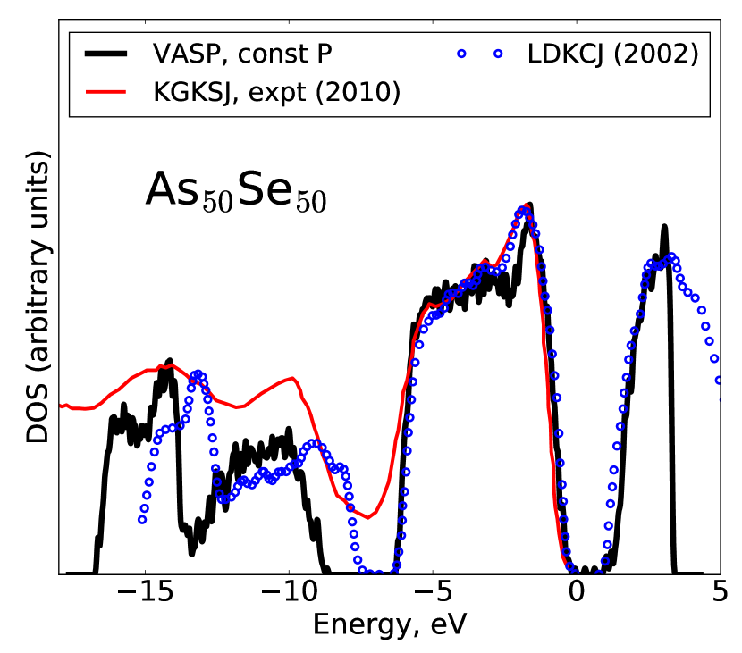
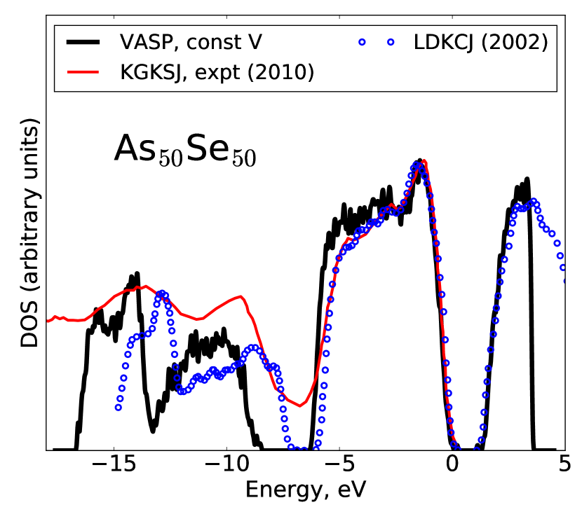
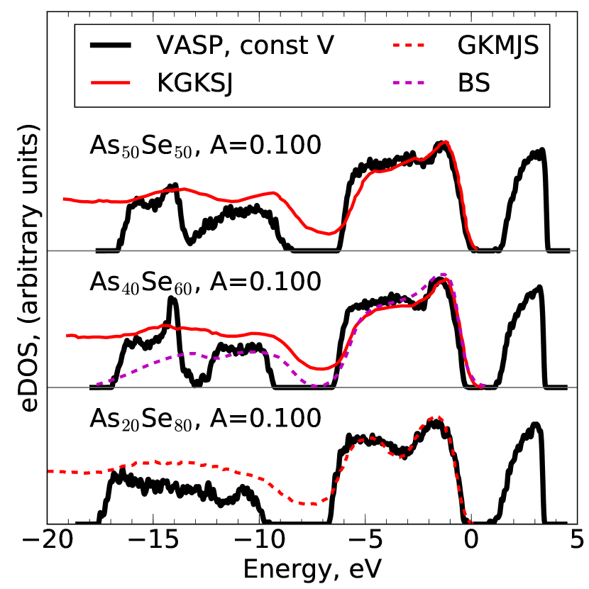
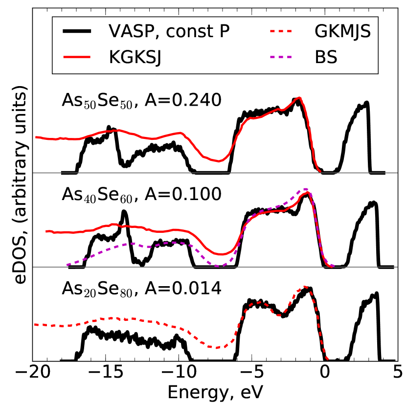
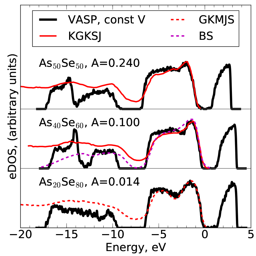
The electronic spectra, as illustrated for several As20Se80 samples in Fig. 2, are overall similar yet clearly vary in detail from sample to sample, and especially so around the forbidden gap. The corresponding figures for the compounds As40Se60 and As50Se50 can be found in the Supplemental Material. There, we also provide an animation that allows one to efficiently survey how the shape and extent of the wave function is correlated with the corresponding energy eigenvalue. The aforementioned sample-to-sample variation is indeed expected for disordered samples. The variation is expected to be relatively small for electronic states sufficiently away from the gap, Anderson (1978) where the density of states is truly continuous and self-averaging. It is this averaged spectrum that is pertinent to experimentally observed absorption spectra because absorption experiments represent a bulk measurement. The electronic density of states averaged over several samples are shown in Fig. 3, along with experimental data, for all three stoichiometries. Clearly, the present results reproduce the gross features found in actual spectra, particularly in the higher energy part of the valence band. The agreement is especially notable for the 20-80 mixture.
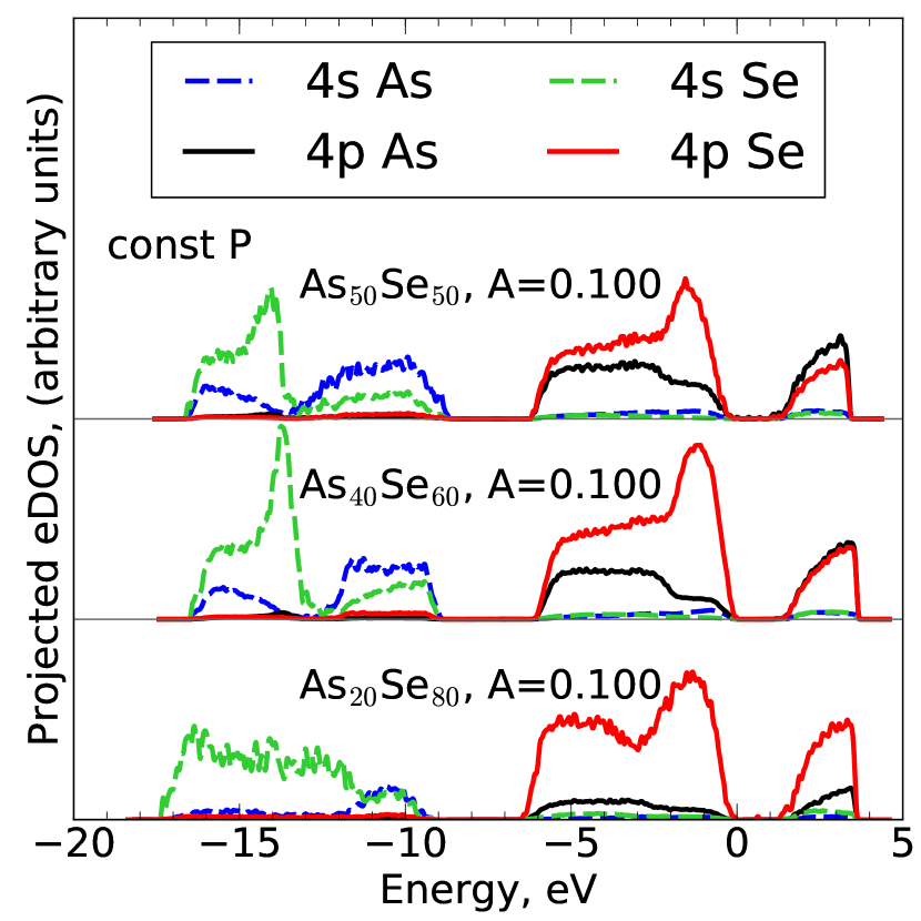
To infer the atomic-orbital makeup of the electronic density of states, we consider the and atomic-orbital contributions to the total density of states as determined using VASP’s built-in projection technique, see Fig. 4. According to the latter Figure, the higher energy portion of the valence band is largely due to the -orbitals. We note that the present spectra for As40Se60 and As50Se50 seem to overestimate the “dip” near -2 eV, which separates the bonding -orbitals from the the selenium-based lone pairs. According to Fig. 4, this may stem from a (modest) underestimation of the density of states corresponding to the As-based -orbitals. The overall good agreement between theory and experiment in this part of the spectrum is reassuring since the bonding is indeed expected to be largely due to the -network. Zhugayevych and Lubchenko (2010c) In contrast with -orbitals, the -orbitals are filled and thus affect the bonding and geometry less directly, via -mixing. Seo and Hoffmann (1999) In the Supplemental Material, we compare the present results with the electronic spectra obtained in two earlier studies, due to Bauchy et al. Bauchy et al. (2014) and Li et al. Li et al. (2002) All methodologies seem to reproduce well the -portion of the spectrum, Li et al.’s results Li et al. (2002) for As50Se50 standing out. There is significantly less agreement with experiment in the -orbital portion.
In contrast with the states comprising the mobility bands, states near the gap are expected to be relatively localized; their quantity and energy should strongly depend on the specific realization. Only upon averaging over many realizations, these localized states should yield a relatively smooth spectrum, which is expected to be exponential. Urbach (1953); Toyozawa (1961); Dow and Redfield (1972); Mahan (1966); Kostadinov (1977); Brezin and Parisi (1980); Cardy (1978); John et al. (1986); Zittartz and Langer (1966); Economou et al. (1970) This is indeed born out by the present data. In view of limited statistics and modest sample sizes, however, it is difficult to determine, based on the spectra alone, which states comprising the individual spectra in Fig. 2 should be assigned to the mobility band and which to the Urbach tails of localized states or, potentially, to the topological midgap states predicted by ZL. Zhugayevych and Lubchenko (2010a, b) This complication makes determination of the width of the forbidden gaps in Fig. 2 ambiguous. In experiment, one conventionally places the edges of the mobility bands at energies corresponding to the onset of the Urbach tail, the latter located by fitting, see Figs. 1 and 2 of Ref. Slusher et al., 2004. The functional form used to fit the Urbach-tail states is:
| (1) |
where stands for the depth of a localized state relative to the edge of the corresponding mobility band, into the gap.
| const | |||||
| As20Se80 | P | 2.00 | 1.91 | 1.84Dahshan et al. (2008), 1.84Ming-Lei et al. (2014) | 0.1 |
| V | 1.71 | 1.74 | 0.1 | ||
| As40Se60 | P | 1.94 | 1.82 | 1.78Slusher et al. (2004), 1.76Behera et al. (2017a), 1.74Felty et al. (1967), 1.64Ming-Lei et al. (2014) | 0.08 |
| V | 1.74 | 1.78 | 0.07 | ||
| As50Se50 | P | 1.94 | 1.60 | 1.74Ming-Lei et al. (2014), 1.72Behera et al. (2017b), [1.64, 1.69, 1.85, 1.76 ]Němec et al. (2005) | 0.27 |
| V | 1.81 | 1.70 | 0.17 |
According to Ref. Slusher et al., 2004, the onset of the exponential tail of the localized states corresponds, by convention, to roughly 1% of the absorption strength characteristic of transitions between bona fide extended states. The full range of absorption strength available in experiment spans a range of at least five orders of magnitude thus permitting one to identify the edge states relatively unambiguously. In contrast, the present DOS barely spans two orders of magnitude. To work around this complication, we employ two distinct methods to assess the gap. In method one, we fit the DOS, near but not exactly at the gap edge, using the functional form and for the valence and conduction band, respectively. Tauc (1974) The square root scaling would be exact for a translationally invariant system in 3D, of course. Kittel (1956) An example of the resulting fit is shown in one of the panels in Fig. 5. (As a practical matter, we obtain the fits by plotting the square of the DOS.) The resulting values of the gap, , are given as in Table 1. We note the apparent deviation of the computed DOS from the simple square-root scaling is consistent with the expectation that the presently generated disordered samples should host localized states.
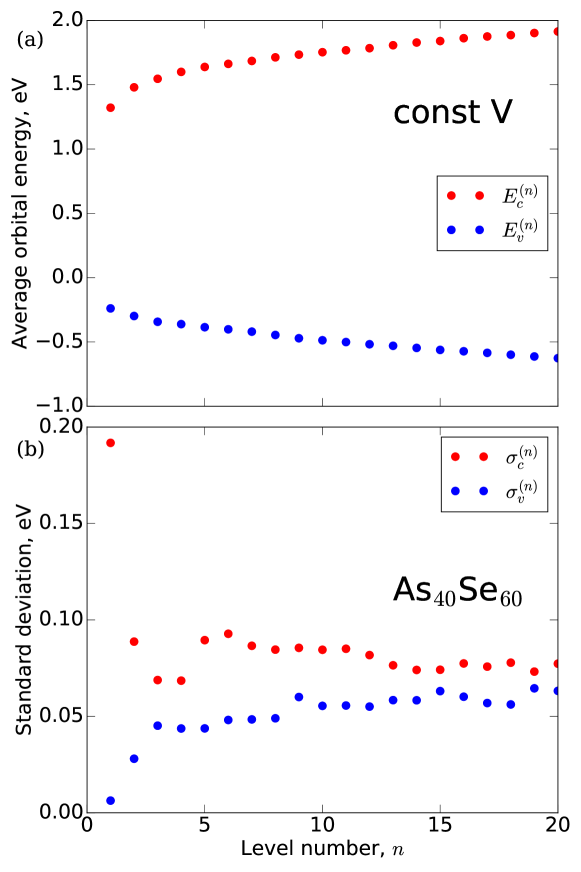
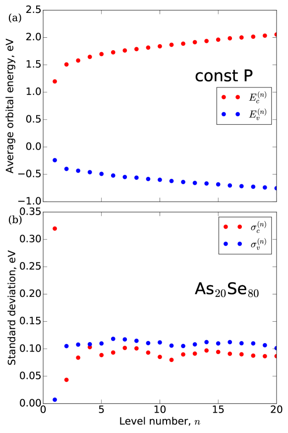
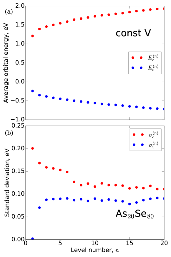
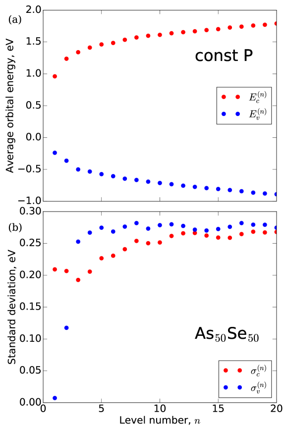
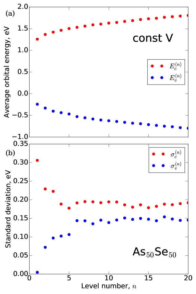
In an alternative strategy, we do not assume any specific functional form for the spectrum either within mobility bands or for the localized states. Instead, we first order the occupied states according to their distance, energy-wise, from the HOMO for each individual sample. Likewise we order, for each sample, the vacant levels according to their separation from the LUMO. Next, we determine the average energy of the -th occupied state and the average energy of the -th empty state. Call the corresponding standard deviations and , respectively. We graph these average energies and the corresponding standard deviations in Fig. 6 for levels 1 through 20. Data for the other stoichiometries, both at constant pressure and volume, can be found in the Supplemental Material. Although the detailed trends of vary somewhat depending on the stoichiometry and the optimization conditions—i.e. const- vs. const-—the following two features are securely reproduced in all cases: (a) The energies () decrease (increase) with . (b) The standard deviations and saturate at large at some value . We also note that is always relatively small, the likely reason being is that the Fermi level is tied to the HOMO.
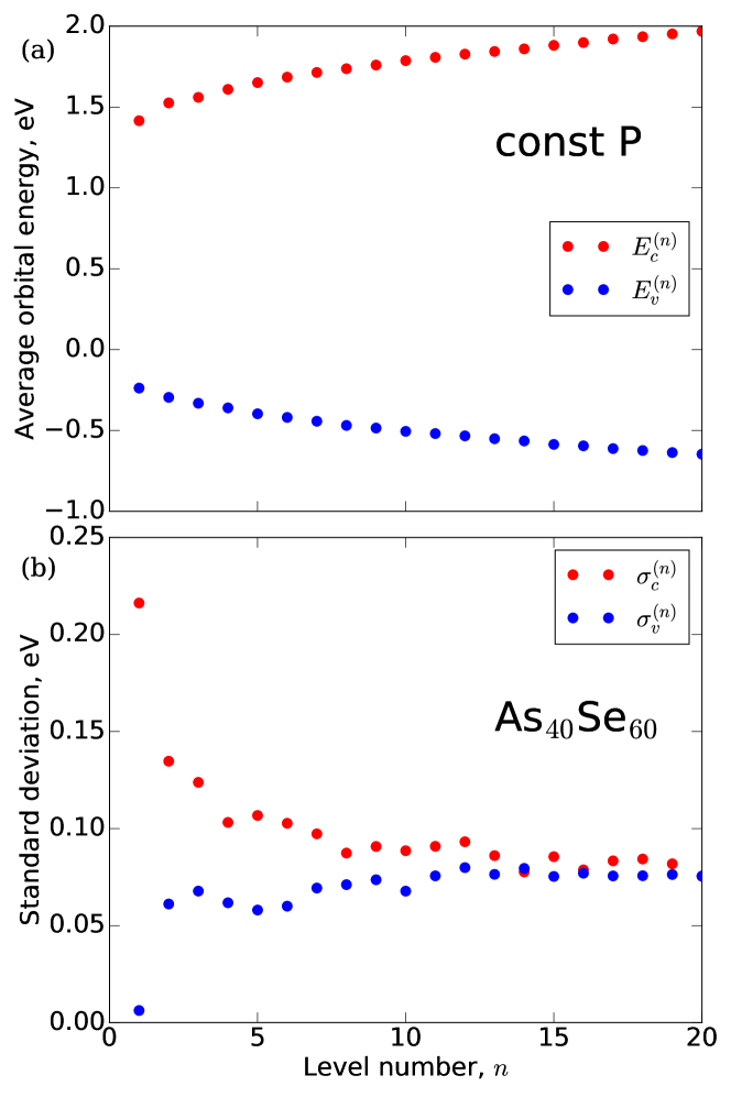
Already the energies of the next-to-HOMO and LUMO levels, , exhibit the amount of variation comparable to the steady value of . At the same time, even if it so happens that these levels belong to the mobility band, they would not be too deep into the band. In addition, there are good reasons to believe the HOMO and LUMO themselves can be sufficiently often associated with the topological midgap states, as we shall see in Section IV. Based on these notions and for the sake of concreteness, we settle on quantifying the band gap using the energy difference between the states:
| (2) |
see Table 1. Given the scatter in the reported experimental values of the gap, the present estimates seem rather satisfactory. Significantly, we observe that the samples optimized at constant pressure reproduce the experimental trend that the gap decreases modestly with arsenic content. (We note that some older data suggest that the gap width, as a function of arsenic content, experiences a shallow “dip” around As43Se57. Street et al. (1978)) In contrast, the const- samples do not follow this trend. Interestingly, samples optimized at constant pressure also did much better Lukyanov and Lubchenko (2017) with regard to the first sharp diffraction peak (FSDP), which is a structural feature. In contrast, const- samples often exhibited a small shoulder instead of a well-defined peak. That the detailed characteristics of the band edges would have a structural signature is consistent with the apparent correlation between the strength of the FSDP, pressure, and the phenomenon of photodarkening. (The term photodarkening Pfeiffer et al. (1991) refers to a light-induced narrowing of the optical gap.) This correlation was discussed in detail in Ref. Lukyanov and Lubchenko, 2017.
We next turn to the standard variation . First we note that for the exponential distribution , the standard deviation is equal to . The number of samples we have generated is too modest to conclusively make out the shape of the distribution of the tail states, as already mentioned. Yet insofar the sampling can be regarded as sufficient to infer the standard deviation, we may associate the quantity with the width parameter of the Urbach tail from Eq. (1). The thus estimated value for the width of the Urbach tail for the stoichiometric compound As40Se60, viz. 0.07-0.08 eV, is consistent with the experimentally reported value of 0.066 eV. Harea et al. (2003) We were unable to find the Urbach energy in the literature for the other two stoichiometries.
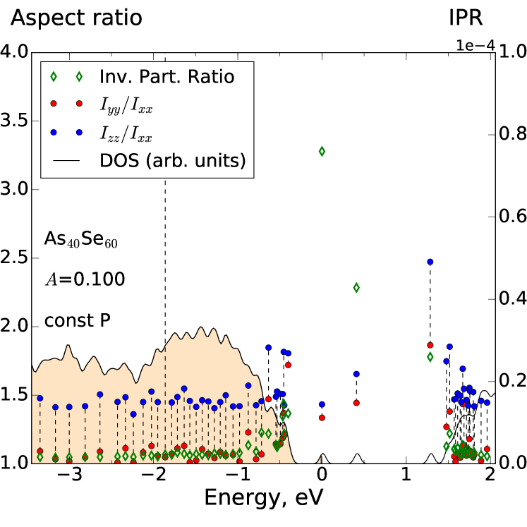
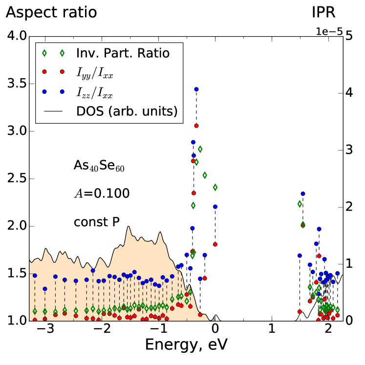
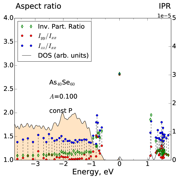
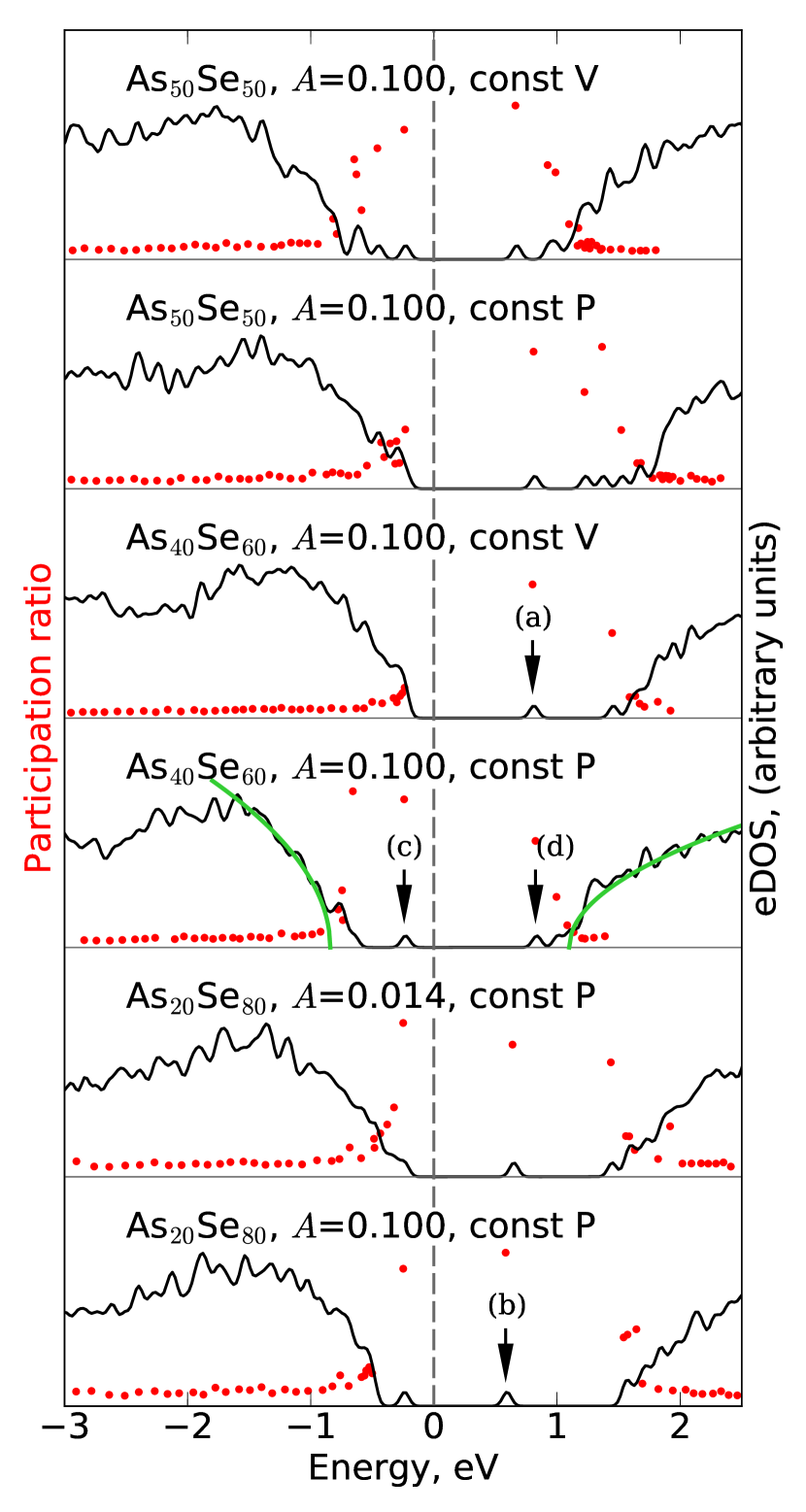
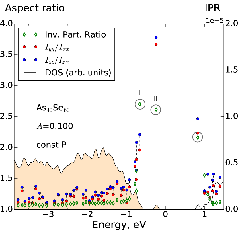
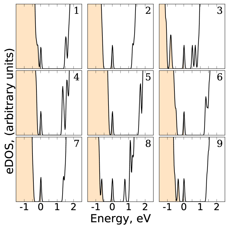
We now turn our attention to the features deep in the mobility gap that are sporadically found in the density of states for specific realizations; these are exemplified in Fig. 5. Note that such sporadic features readily become part of the background upon averaging, as in Fig. 3. While our statistics are clearly limited, examination of the available spectra for individual realizations, Fig. 2 and Figs. S3 and S4 in the Supplemental Material, suggest that roughly only one in ten samples display such deep midgap states already in the stoichiometric compound As40Se60, the number of incidents seemingly increasing away from the exact 2:3 stoichiometry. We immediately point out that on purely statistical grounds, observing a midgap state like that in Fig. 14 is not at all likely. Indeed, given that the width of the Urbach tail is numerically close to eV, our chances of observing that midgap state are roughly one in in view of Eq. (1). That is, roughly one per thousand samples.
Note that the defect-like midgap states in Fig. 2 and 5 are unforced in that the samples contain an even number of electrons and are fully geometrically optimized; no broken bonds are deliberately put in the system. Conversely we note that when occupied, such deep states are very costly—at up to per state, viz. ca. 2 eV, and thus would be presumably stabilized during geometric optimization unless prevented from doing so for some special reason. Zhugayevych and Lubchenko Zhugayevych and Lubchenko (2010a, b) (ZL) have argued exactly such a reason exists in glassy chalcogenides. The reader is referred to those publications for detailed discussion. In the following Section, we briefly reiterate some of those notions and present new results that will be helpful in interpreting some of the midgap-state features revealed in this study.
III The topological electronic midgap states: General results
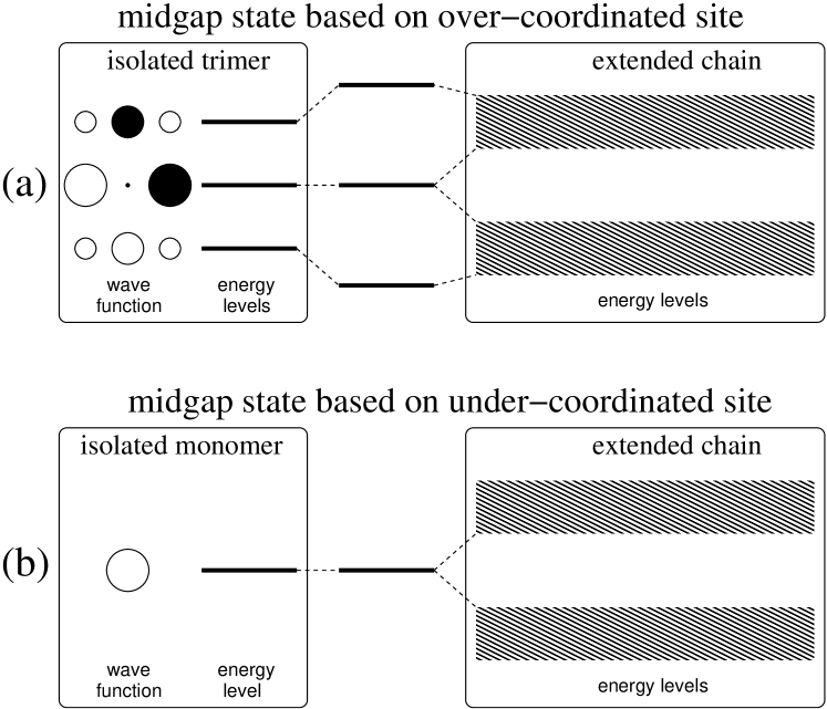
ZL have argued Zhugayevych and Lubchenko (2010a) that at some places along the domain walls separating regions occupied by distinct aperiodic free energy minima in a glassy liquid, local coordination will differ from its optimal value. The missing or extra bond should be perpendicular to the domain wall. Specifically in the chalcogenides, quasi-one-dimensional chain-like motifs can be identified Zhugayevych and Lubchenko (2010b) based on a structural model, Zhugayevych and Lubchenko (2010c) in which these materials are regarded as distorted, symmetry-broken version of more symmetric parent structures locally defined on a simple cubic lattice. In the simplest case, a defect-free distorted chain exhibits an exact alternation pattern of a covalent bond and a secondary interaction and can be thought of as a chain of weakly interacting dimers. At a malcoordination defect, one atom or more will be have one too many or one too few bonds. As was understood in the context of conjugated polymers,Heeger et al. (1988); Brazovskii and Kirova (1981) such malcoordination defects must host very special midgap electronic states, see illustration in Fig. 7. If singly occupied and close to the middle of the gap, they formally correspond with a neutral particle that has spin 1/2, see Fig. 7(a). (The electron charge is exactly compensated by the polarization of the lattice.) The deviation of the bond length from its value in a perfectly dimerized chain shows a sigmodal dependence on the coordinate. The strain has a solitonic profile, hence the midgap states are often called “solitonic.”
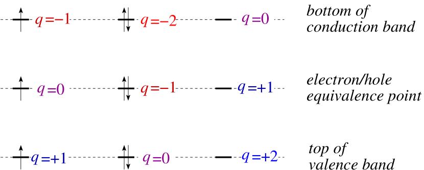
In the chalcogenides, one expects that most of the midgap states would be either fully occupied or empty: On the one hand, the chalcogenides exhibit spatial variation in the electronegativity. Suppose the variation is on average equal to . Then a midgap state based on the more electronegative site is typically lowered, energy-wise, by the amount relative to the middle of the gap. Likewise, defects centered on the less electronegative element would be destabilized by the same amount. In addition, one expects that a singly occupied midgap state will be modestly stabilized by binding an electron or hole Zhugayevych and Lubchenko (2010a)—consistent with simple electron counting arguments. Zhugayevych and Lubchenko (2010b) These notions are summarized in Fig. 7(b). The apparent charge of the defect will depend not only on the occupation of the midgap state but also on its position in the band, Rice and Mele (1982) see the informal chart in Fig. 8.
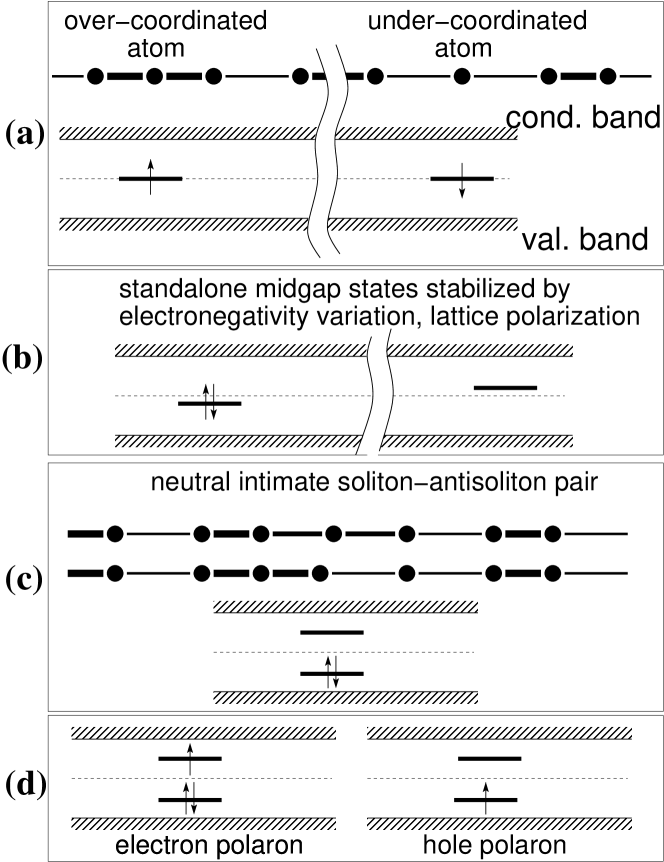
A midgap state cannot be removed by elastic deformation but, instead, only via annihilation with a defect of opposite malcoordination, which resides on the same chain. For this reason, such oppositely malcoordinated configurations are often called soliton and anti-soliton. When the spatial separation between such oppositely malcoordinated defects is small, the respective energy levels form a resonance. The lower level of the resonance becomes occupied, the upper level vacant, as in Fig. 7(c), where we also sketch the corresponding structural motifs. Once the defects fully recombine, the bottom level merges with the valence band and the top level with the conduction band. We note that odd-numbered cyclic ring molecules at half-filling must host at least one defect that in principle cannot be removed. The latter will thus host a midgap state which is singly-occupied. Finally, Fig. 7(d) schematically shows what happens when an electron or hole is added to a chain and the system is allowed to relax to form a polaron. In contrast with a continuum view, in which a polaron can be thought of as a generic impurity-like state, the lattice deformation results in the appearance of at least two midgap states. The resulting configuration can be thought of as a charged soliton in a close proximity with a neutral soliton, Heeger et al. (1988) or a charge carrier bound to an intimate soliton-antisoliton pair.
A distinct feature of the midgap states is their shape: Since the wavefunctions of the topological states are hosted by chain-like dimensional motifs, they are relatively localized in the direction perpendicular to the motif, but could be substantially delocalized along the motif itself. The delocalization along the chain is surprisingly large given how deep the states are. This is because the localization length is no longer determined by the depth of the state but, instead, by the ratio of the transfer integrals of the strong and weak bond. The amount of delocalization is additionally increased because the malcoordination is smoothly distributed over the chain, typically over ten bond lengths or so, see the Supplementary Material for more detail and Ref. Zhugayevych and Lubchenko, 2010b for specific molecular realizations. It was argued in that work that the effect of the solid matrix housing the chain is, largely, to renormalize the on-site energies and electronic transfer integrals along the chain. Here we revisit this proposition by considering two or more chains crossing at one site. One can think of one chain as made, for instance, primarily of -bonded orbitals and the other chain of -bonded orbitals. Exactly one of the chains hosts a malcoordination defect by construction. A graphical illustration of this set-up is shown in Fig. 9, panels (a) and (b) corresponding to over-coordination and under-coordination, respectively. The chains are depicted as parallel to avoid crowding the picture, however they are not parallel in the physical space. The transfer integral between the two orbitals at the intersection between the chains is denoted with . These two orbitals belong to the same atom; the non-zero overlap between the orbitals can come about because the chains are not exactly perpendicular and/or because -mixing is present. For simplicity, we allow the bond lengths to have only two values. These values would correspond to the covalent and secondary bond in a perfectly dimerized chain; the electronic hopping integrals are and () for the covalent and secondary bond, respectively. Also for simplicity, we set all of the on-site energies at the same value . The results can be straightforwardly generalized for a non-vanishing, sign-alternating on-site energy. Rice and Mele (1982); Zhugayevych and Lubchenko (2010b) The latter situation would be directly relevant to linear chain-like motifs in which chalcogen and pnictogen alternate in sequence. Finally, we set transfer integrals for next-nearest and farther neighbors at zero.
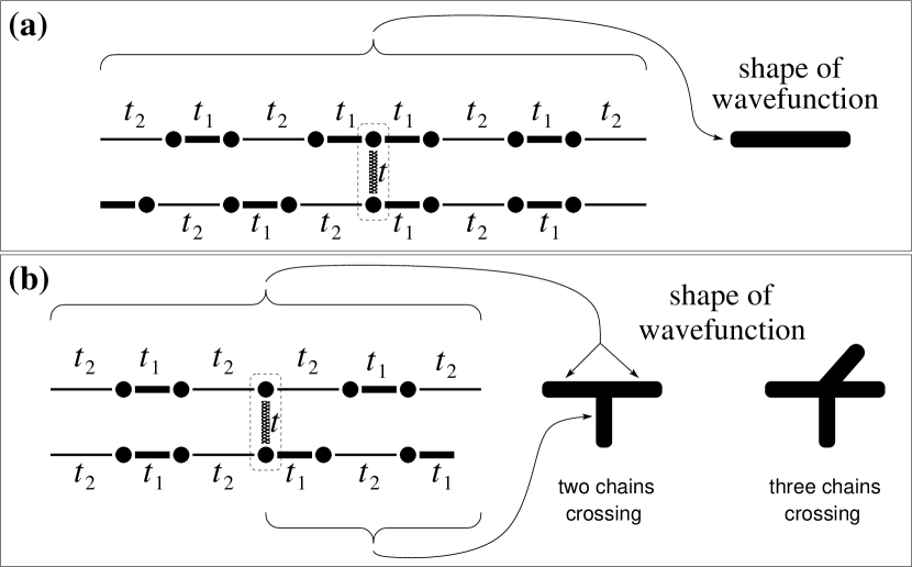
The resulting Hamiltonian is easily numerically diagonalized, the corresponding spectra and the midgap wave-functions shown in Figs. 10 and 11. We observe that in the case of overcoordination, the wave-function is confined to the chain housing the defect, consistent with the analysis of Zhugayevych and Lubchenko. Zhugayevych and Lubchenko (2010c, b) In contrast, when the midgap state is caused by under-coordination, a substantial part of the the wave function now “spills” into the crossing, defect-free chains. We notice that the wavefunction of the midgap state, on such a defect-free chain, is non-vanishing only on one side of the intersection. We have directly checked that the same conclusions apply when three chains intersect. In cases when the wavefunction of the midgap state is shared between a number of intersecting chains, its shape can be thought of as a set of linear portions emanating from the same lattice site; only two of these portions are expected to be approximately co-linear.
These contrasting behaviors with respect to the wavefunction’s shape are discussed formally in the Supplemental Material, but can be rationalized already using the following, informal line of reasoning, which is graphically illustrated in Fig. 12. In the absence of geometric optimization, which would distribute the malcoordination over an extended portion of the chain, an over-coordinated center can be thought of as a trimer weakly coupled to a perfectly dimerized chain via two weak bonds, as in Fig. 12(a). The bottom and top level of the trimer will be, respectively, stabilized and destabilized as a result of the coupling. The non-bonding state of the trimer, on the other hand, will remain in the middle of the gap by symmetry, since it is coupled equally strongly to both the bottom and top band of the chain. The corresponding wavefunction vanishes at the central site of the trimer, either without or with coupling.
In contrast, an under-coordinated center in a non-relaxed geometry can be thought of as a single orbital at coupled to a perfectly dimerized chain, as in Fig. 12(b). The wave function of the resulting midgap state will be non-zero and, in fact, will have its largest value at that orbital. When a defected chain is coupled to a perfectly dimerized chain, the electron will be also able to tunnel to some extent into the dimerized chain, but will do so only on one side. This is because a state inside the forbidden gap must have a wavefunction that is either exponentially increasing or decreasing function of the coordinate. In a perfectly dimerized chain, either behavior would have to be maintained throughout; the resulting wavefunction would not be normalizable. This notion can be made formal, see the Supplemental Information. There we also show that the above conclusions still apply, even if one allows the chain to geometrically optimize.
The question of what should happen to a midgap state when the chain is enclosed in a solid matrix is much more complicated than the above setup where only two or three chains intersect. The solid can be thought of as a very large number of closed chains that cross at the defect site; the resulting interference effects could be significant. We have conducted preliminary tests on the effects of an ordered solid matrix using small slabs of crystalline As2Se3, see the Supplemental Material. We observed that even after the sample is allowed to geometrically optimize, the midgap state remains robustly within the gap and, in fact, moves closer to the gap’s center. The wavefunction of midgap state tends to peak at the slab’s surface while its shape becomes more anisotropic following geometric optimization.
IV The topological midgap states: Present samples
Motivated by the notions made in Section III, we next quantify both the extent and compactness of states within the gap and its immediate vicinity. A concrete way to quantify the localization of an orbital is to compute the so called inverse participation ratio (IPR):
| (3) |
where the denominator is included in case the orbital is not normalized to unity. A moment thought shows that the above expression generically scales as the inverse volume of the region occupied by the orbital. Thus the inverse participation ratio gives a volumetric measure of localization of the respective wavefunction. The so evaluated measure of localization is shown with the red dots in Fig. 5. Consistent with expectation, the states comprising the mobility band are delocalized over the whole sample. There may be an ever so slight increase in localization going toward the gap. This increase picks up closer to the edge of mobility band so that by the end of the Urbach tail, the states are seen to occupy a volume that is about one order of magnitude less than the extended states. (This difference depends on the sample size, of course.) We observe that the overall degree of localization of the deep midgap states is greater still than that of the Urbach states, but not dramatically so.
To assess the shape of the wavefunctions, we compute its “tensor of inertia” according to:
| (4) |
where is the charge density at a point . There is a technical complication in computing the above quantity since the sample is periodically continued, by construction, and so one must make a decision as to the precise location of the repeat unit so that the wavefunction is most connected and, hence, compact. After choosing the optimal location for the centroid of the wavefunction, we compute the corresponding inertia tensor and bring it to a diagonal form. We next sort the resulting principal moments of inertia in ascending order and label them as follows: . Since here we are interested only in the shape, not the absolute extent of the wavefunction, we consider only the aspect ratios of and . According to the ZL predictions, these ratios should significantly exceed unity at least for the midgap states that are confined to one chain. One may also generically expect the aspect ratio to be numerically close to one for the extended states within the mobility bands.
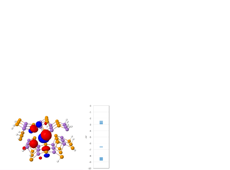
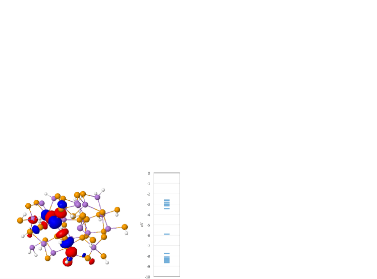
These expectations are well borne out by our data, which are displayed in Fig. 14. We observe that the aspect ratio largely echoes the participation ratio: The deeper inside the gap, the more non-compact the wavefunctions tend to be. Again, the difference between the deep-midgap and Urbach states is substantial but not dramatic. It is instructive to visualize some of those deep midgap states. We have selected four representative examples shown in Fig. 15; the location of these states in the respective electronic spectra can be found in Fig. 5.
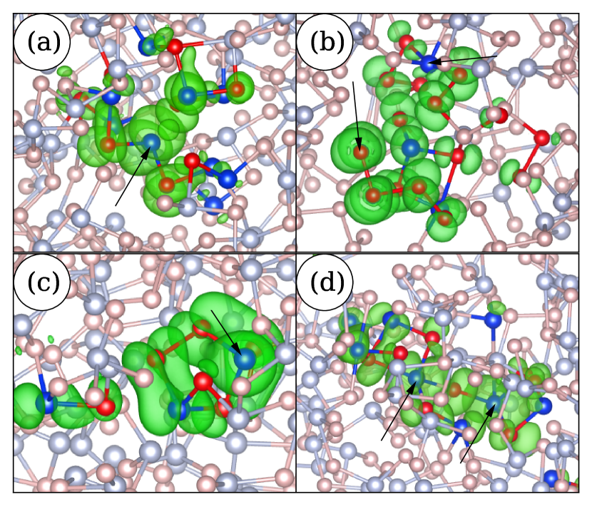
We observe that at least in the cases encountered in the present study, the wavefunctions of non-extended states are rather anisotropic, and more so the deeper the corresponding state is into the mobility gap. While this is consistent with the general analysis of ZL, Zhugayevych and Lubchenko (2010b) the atomic motifs housing the wavefunctions in the present study are significantly more complex than the standalone molecular liner motifs generated by ZL. In any event, all of the motifs in Fig. 15 contain at least one malcoordinated atom. Specifically, motif (a) contains an under-coordinated arsenic, (b) under-coordinated selenium and over-coordinated arsenic, (c) an under-coordinated arsenic, and (d) two over-coordinated arsenics. Consistent with the discussion in Section III, the midgap state wavefunction stemming from under-coordination in panel (a) appears to branch out, while the defect in (d) contains over-coordinated atoms and is elongated preferentially in one spatial direction. Defect (c) is notable in that the bulk of electron density resides on a 5-member closed ring. As mentioned earlier, such odd-numbered rings must host midgap states.
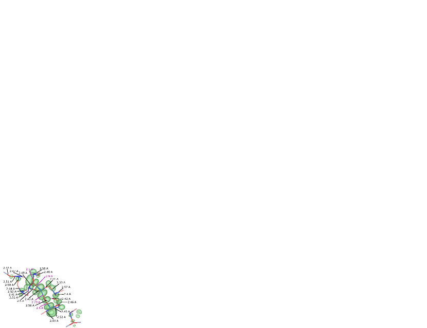
We note that when quasi-linear, the midgap states recovered in the present study are more complicated objects than what was foreseen by ZL predictions. Zhugayevych and Lubchenko (2010b) To illustrate this notion, we provide in Fig. 16 a different view of the quasi-linear midgap wavefunction from panel (d). In Fig. 16, we have highlighted the bonds connecting the atoms that contribute significantly to the wavefunction. Importantly, the bond lengths along the bulk portion of the wavefunction, highlighted in purple, significantly exceed the length of the covalent As-Se bond, i.e. 2.4 Å. Lukyanov and Lubchenko (2017) That the bond length near a topological defect should have an intermediate value between than for the covalent and secondary bond is a hallmark feature of the midgap states. Zhugayevych and Lubchenko (2010a, b) These bonds clearly form a continuous, chain-like pattern. In addition, we observe a “satellite” portion of the wavefunction running alongside its primary portion. This satellite portion evidently has a substantial contribution from lone pairs and likely stems from mixing between the -orbitals that are, respectively, parallel and perpendicular to the line of the defect.
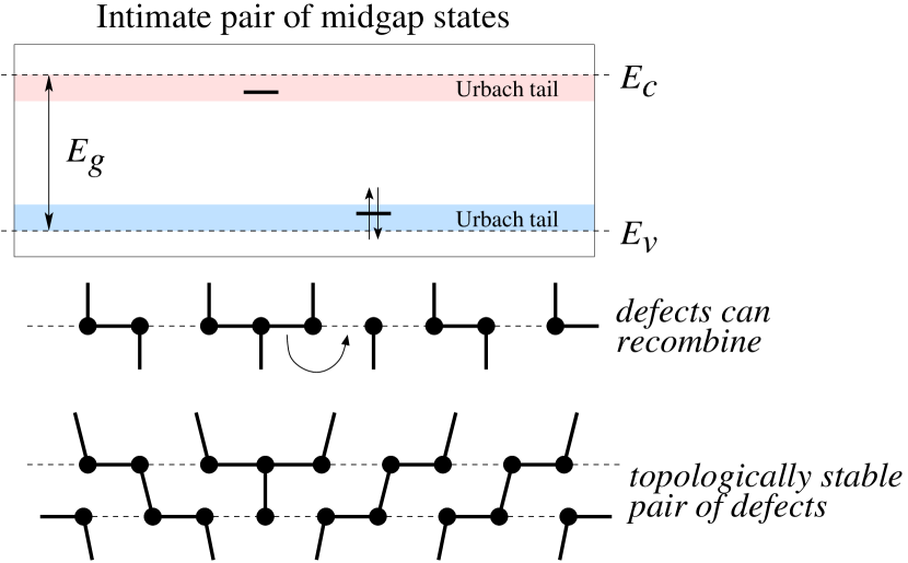
If standalone, a filled state that is close to the center of the gap would be similar to the negatively charged topological state from Fig. 7(b). On the other hand, we observe that vacant midgap states are also generally present in the same sample implying that the just mentioned filled state may, instead, be the lower level of a resonance formed by two or more neutral midgap states, as in Fig. 7(c). There appears to be no conclusive way to distinguish between those situations in the present computational setup since in such modestly-size samples, it might be difficult to produce even a relatively isolated, let alone truly standalone defect. The situation is however clearer with the filled states close to the valence band, i.e., the Urbach states, since they certainly have vacant counterparts close to the conduction band. Thus in view of Fig. 7(c), one may think of the Urbach states as resulting from intimate soliton-antisoliton pairs. This notion adds quite a bit of microscopic detail to the conventional idea of Urbach-tail states as a generic consequence of disorder. Indeed, we observe in Fig. 14 that the characteristics of a filled state change only gradually with the energy of the state. Thus the Urbach states share, to an extent, some of the properties with the deep midgap states, such as the anisotropy in shape.
We have observed above that very deep midgap states spontaneously arise in some samples and match the characteristics of the topological midgap states predicted by Zhugayevych and Lubchenko. Next we study what happens when the system is forced to have at least one dangling bond, which can be accomplished by using an odd number of electrons. Because selenium and arsenic have an even and odd number of electrons, respectively, we can ensure that the system has at least one unpaired spin—and hence a dangling bond—by using an odd number of arsenic atoms. This we accomplish by removing one of the arsenic atoms from a sample that contains an even number of such atoms using three distinct protocols: In protocol (I) we remove an arsenic atom randomly from a sample that has been already geometrically optimized. No further optimization is performed. In protocol (II), we further optimize the sample obtained in protocol (I). In protocol (III), one arsenic atom is removed already from the parent structure. Only after this is the structure geometrically optimized. The logic behind these protocols is as follows: In protocol (I), we expect the defect to be as close as possible in character to a vacancy. In protocol (II), we allow this “vacancy” to relax but subject to an environment that is already mechanically stable. In protocol (III) the system is given the greatest amount of freedom to relax afforded by the structure-building algorithm in Ref. Lukyanov and Lubchenko (2017) The amount of residual strain in the structure is expected to be the greatest in structures of type I and the least in structures of type III. Everywhere below, we limit ourselves to the stoichiometric compound As0.4Se0.6. (The stoichiometry is obeyed only approximately.)
The electronic density of states for individual realizations for all three protocols is illustrated in Fig. 17, alongside that for the original structure that contained an even number of electrons. We observe that the gross features of the electronic spectrum are not sensitive to the detailed preparation protocol.
We next focus on the electronic density of states within the mobility gap and its immediate vicinity. Nine realizations for protocols I, II, and III are shown, respectively in Figs. 18, 19, and 20. In all figures, shading indicates filled levels. Consistent with the expectation that samples of type I should exhibit most strain, such samples show on average the greatest number of midgap states. Yet even though samples of type II and III are allowed to relax, some of them still host very deep-lying midgap states. We observe that the midgap states in some samples of type I are similar, at least superficially, to the hole-polaron configuration in Fig. 7(d), see for instance panel 8. This result is perhaps not too surprising since the region centered on the removed arsenic atom has a lower electron density or, equivalently, increased hole density. In contrast, samples of type II seem to house primarily neutral states from Fig. 7(a). Samples of type (III) exhibit such states as well and, in addition, states similar to the electron-polaron states from Fig. 7(d), as in panel 9. While it seems reasonable that structures of type III would exhibit the highest electron density of the three structure types, it is not at all obvious why electron-polaron-like configurations should be so stable as to be readily found already in the small ensemble structures we have generated in the present study.
Finally we refer the reader to the Supplemental Material for the information on the localization and anisotropy of the electronic states for systems with an odd number of electrons, which is presented there in the format of Fig. 14. The main conclusion is that the midgap states with systems with an odd-number of electrons are entirely analogous to systems with filled states. In a distinction, the midgap states in systems of type I are significantly more localized than when the sample is allowed to relax. This is expected since upon relaxation, the lone pair residing in the cavity formed by removing an atom is able to mix more readily with the rest of the orbitals.
V Summary
We have computationally-generated samples of glassy arsenic selenide, for several stoichiometries, that appear to exhibit all putative types of electronic states thought to exist in these materials. The gross features of the electronic density of states do not vary from sample to sample. The corresponding portions of the density of states are attributed to the mobility bands; these states are extended and their density of states is self-averaging. In contrast, states near the edge of the mobility bands strongly fluctuate in energy. The statistics of this variation match well the distribution of the venerable Urbach-tail states.
Most significantly, we recover a special set of electronic states whose characteristics match those of the topological midgap states predicted earlier by Zhugayevych and Lubchenko (ZL). These special midgap states are very deep into the mobility gap and are not simply a generic consequence of static disorder in the atomic position. Instead, they stem from the vast degeneracy of the free energy landscape of a glassy liquid. The midgap states have been predicted Zhugayevych and Lubchenko (2010b) to reside on domain walls separating distinct minima on the free energy landscape. We have shown that in addition to the chain-like shape for the midgap states predicted in Ref. Zhugayevych and Lubchenko (2010b), more complicated, urchin-like and cyclic shapes are possible, too.
Different charge states of the midgap states have been observed that could be potentially identified with standalone midgap states or their intimate pairs, and also with added charge carriers. Clearly, such polaron-like states are significant in the context of the mechanism of electrical conductance in amorphous chalcogenides. The current view is that in the chalcogenides, electrical current is carried by small polarons, Emin (1983a, b) each of which can be thought of as compound particle consisting of a charge carrier proper and the polarization of the lattice, largely in the spirit of the Born model of solvation of charge in a polar solvent. In contrast with the continuum Born picture, the present treatment directly identifies sets of orbitals that house the charge carrier. Such sets greatly exceed in size and complexity what would be expected of a small polaron. The present results also indicate that the polarization of the lattice involves very particular changes in local bonding such as emergence of malcoordination.
The above findings were enabled by the availability of a quantum-chemical approximation that recovers the width of the mobility gap with reasonable accuracy, viz., a specific flavor of a hybrid DFT approximation. Standard DFT approaches tend to underestimate the width of the gap thus effectively concealing many of the features of the electronic spectrum this work focused on.
We hope that a more conclusive identification of the presently reported deep midgap states with the topological midgap states predicted by ZL will be possible when we learn how to simulate transitions between distinct free energy minima in a glassy chalcogenide or similar compounds. When approached directly, such a simulation is computationally very costly because of excessively high relaxation barriers. Lubchenko (2015) Circumventing this complication is work in progress.
VI Acknowledgments
This work has been supported by the National Science Foundation Grants CHE-0956127, CHE-1465125, and the Welch Foundation Grant E-1765. We gratefully acknowledge the use of the Maxwell/Opuntia Cluster and the untiring support from the Center for Advanced Computing and Data Systems at the University of Houston. Partial support for this work was provided by resources of the uHPC cluster managed by the University of Houston and acquired through NSF Award Number ACI-1531814.
References
- Anderson (1958) P. W. Anderson, Phys. Rev. 109, 1492 (1958).
- Mott (1982) N. Mott, Proc. R. Soc. Lond. A 382, 1 (1982).
- Cohen et al. (1969) M. H. Cohen, H. Fritzsche, and S. R. Ovshinsky, Phys. Rev. Lett. 22, 1065 (1969).
- Mott (1990) N. F. Mott, Metal-Insulator Transitions (Taylor and Francis, London, 1990).
- Emin (1983a) D. Emin, Comments Solid State Phys. 11, 35 (1983a).
- Emin (1983b) D. Emin, Comments Solid State Phys. 11, 59 (1983b).
- Urbach (1953) F. Urbach, Phys. Rev. 92, 1324 (1953).
- Toyozawa (1961) Y. Toyozawa, Progr. Theor. Phys. 26, 29 (1961).
- Dow and Redfield (1972) J. D. Dow and D. Redfield, Phys. Rev. B 5, 594 (1972).
- Mahan (1966) G. D. Mahan, Phys. Rev. 145, 602 (1966).
- Kostadinov (1977) I. Z. Kostadinov, J. Phys. C: Solid State Phys. 10, L263 (1977).
- Brezin and Parisi (1980) E. Brezin and G. Parisi, J. Phys. C 13, L307 (1980).
- Cardy (1978) J. L. Cardy, J. Phys. C 11, L321 (1978).
- John et al. (1986) S. John, C. Soukoulis, M. H. Cohen, and E. N. Economou, Phys. Rev. Lett. 57, 1777 (1986).
- Zittartz and Langer (1966) J. Zittartz and J. S. Langer, Phys. Rev. 148, 741 (1966).
- Economou et al. (1970) E. N. Economou, S. Kirkpatrick, M. H. Cohen, and T. P. Eggarter, Phys. Rev. Lett. 25, 520 (1970).
- Lubchenko and Wolynes (2004) V. Lubchenko and P. G. Wolynes, J. Chem. Phys. 121, 2852 (2004).
- Lubchenko and Wolynes (2018) V. Lubchenko and P. G. Wolynes, J. Phys. Chem. B 122, 3280 (2018).
- Anderson (1976) P. W. Anderson, J. Phys. (Paris) C4, 339 (1976).
- Zhugayevych and Lubchenko (2010a) A. Zhugayevych and V. Lubchenko, J. Chem. Phys. 132, 044508 (2010a).
- Biegelsen and Street (1980) D. K. Biegelsen and R. A. Street, Phys. Rev. Lett. 44, 803 (1980).
- Hautala et al. (1988) J. Hautala, W. D. Ohlsen, and P. C. Taylor, Phys. Rev. B 38, 11048 (1988).
- Shimakawa et al. (1995) K. Shimakawa, A. Kolobov, and S. R. Elliott, Adv. Phys. 44, 475 (1995).
- Bishop et al. (1977) S. G. Bishop, U. Strom, and P. C. Taylor, Phys. Rev. B 15, 2278 (1977).
- Mollot et al. (1980) F. Mollot, J. Cernogora, and C. Benoit à la Guillaume, Phil. Mag. B 42, 643 (1980).
- Tada and Ninomiya (1989a) T. Tada and T. Ninomiya, Sol. St. Comm. 71, 247 (1989a).
- Tada and Ninomiya (1989b) T. Tada and T. Ninomiya, J. Non-Cryst. Sol. 114, 88 (1989b).
- Tada and Ninomiya (1989c) T. Tada and T. Ninomiya, J. Non-Cryst. Sol. 137&138, 997 (1989c).
- Kolomiets (1981) B. T. Kolomiets, J. Phys. (Paris) C4 42, 887 (1981).
- Mott (1993) N. F. Mott, Conduction in Non-crystalline Materials (Clarendon Press, Oxford, 1993).
- Anderson (1975) P. W. Anderson, Phys. Rev. Lett. 34, 953 (1975).
- Street and Mott (1975) R. A. Street and N. F. Mott, Phys. Rev. Lett. 35, 1293 (1975).
- Kastner et al. (1976) M. Kastner, D. Adler, and H. Fritzsche, Phys. Rev. Lett. 37, 1504 (1976).
- Vanderbilt and Joannopoulos (1981) D. Vanderbilt and J. D. Joannopoulos, Phys. Rev. B 23, 2596 (1981).
- Li and Drabold (2000) J. Li and D. A. Drabold, Phys. Rev. Lett. 85, 2785 (2000).
- Zhugayevych and Lubchenko (2010b) A. Zhugayevych and V. Lubchenko, J. Chem. Phys. 133, 234504 (2010b).
- Pyykkö (1997) P. Pyykkö, Chem. Rev. 97, 597 (1997).
- Xia and Wolynes (2000) X. Xia and P. G. Wolynes, Proc. Natl. Acad. Sci. U. S. A. 97, 2990 (2000).
- Lubchenko and Wolynes (2001) V. Lubchenko and P. G. Wolynes, Phys. Rev. Lett. 87, 195901 (2001).
- Lubchenko and Wolynes (2007) V. Lubchenko and P. G. Wolynes, Annu. Rev. Phys. Chem. 58, 235 (2007).
- Lubchenko (2015) V. Lubchenko, Adv. Phys. 64, 283 (2015).
- Lubchenko (2006) V. Lubchenko, J. Phys. Chem. B 110, 18779 (2006).
- Rabochiy and Lubchenko (2012) P. Rabochiy and V. Lubchenko, J. Phys. Chem. B 116, 5729 (2012).
- Heeger et al. (1988) A. J. Heeger, S. Kivelson, J. R. Schrieffer, and W. P. Su, Rev. Mod. Phys. 60, 781 (1988).
- Vanderbilt and Joannopoulos (1980) D. Vanderbilt and J. D. Joannopoulos, Phys. Rev. B 22, 2927 (1980).
- Zhugayevych and Lubchenko (2010c) A. Zhugayevych and V. Lubchenko, J. Chem. Phys. 133, 234503 (2010c).
- Golden (2016) J. C. Golden, SYMMETRY BREAKING IN CHEMICAL INTERACTIONS, Ph.D. thesis, University of Houston (2016).
- Lukyanov and Lubchenko (2017) A. Lukyanov and V. Lubchenko, J. Chem. Phys. 147, 114505 (2017).
- Parisi and Zamponi (2010) G. Parisi and F. Zamponi, Rev. Mod. Phys. 82, 789 (2010).
- Deschamps et al. (2015) M. Deschamps, C. Genevois, S. Cui, C. Roiland, L. LePollès, E. Furet, D. Massiot, and B. Bureau, J. Phys. Chem. B 119, 11852 (2015).
- Elliott (1991) S. R. Elliott, Nature 354, 445 (1991).
- Salmon et al. (2005) P. S. Salmon, R. A. Martin, P. E. Mason, and G. J. Cuello, Nature 435, 75 (2005).
- Bauchy et al. (2014) M. Bauchy, A. Kachmar, and M. Micoulaut, J. Chem. Phys. 141, 194506 (2014).
- Perdew and Levy (1983) J. Perdew and M. Levy, Physical Review Letters 51, 1884 (1983).
- Sham and Schlütter (1983) L. Sham and M. Schlütter, Physical Review Letters 51, 1888 (1983).
- Brazovskii and Kirova (1981) S. Brazovskii and N. Kirova, JETP Lett. 33, 4 (1981).
- Kresse and Hafner (1993) G. Kresse and J. Hafner, Phys. Rev. B 47, 558 (1993).
- Kresse and Hafner (1994) G. Kresse and J. Hafner, Phys. Rev. B 49, 14251 (1994).
- Kresse and Furthmüller (1996a) G. Kresse and J. Furthmüller, Comput. Mat. Sci. 6, 15 (1996a).
- Kresse and Furthmüller (1996b) G. Kresse and J. Furthmüller, Phys. Rev. B 54, 1169 (1996b).
- Perdew et al. (1992) J. P. Perdew, J. A. Chevary, S. H. Vosko, K. A. Jackson, M. R. Pederson, D. J. Singh, and C. Fiolhais, Phys. Rev. B 46, 6671 (1992).
- Perdew et al. (1993) J. P. Perdew, J. A. Chevary, S. H. Vosko, K. A. Jackson, M. R. Pederson, D. J. Singh, and C. Fiolhais, Phys. Rev. B 48, 4978 (1993).
- Kozyukhin et al. (2011) S. Kozyukhin, R. Golovchak, A. Kovalskiy, O. Shpotyuk, and H. Jain, Физика и техника полупроводников 45, 433 (2011).
- Golovchak et al. (2007) R. Golovchak, A. Kovalskiy, A. C. Miller, H. Jain, and O. Shpotyuk, Phys. Rev. B 76, 125208 (2007).
- Bishop and Shevchik (1975) S. Bishop and N. Shevchik, Phys. Rev. B 12, 1567 (1975).
- Anderson (1978) P. W. Anderson, Rev. Mod. Phys. 50, 191 (1978).
- Seo and Hoffmann (1999) D. Seo and R. Hoffmann, J. Sol. State Chem. 147, 26 (1999).
- Li et al. (2002) J. Li, D. Drabold, S. Krishnaswami, G. Chen, and H. Jain, Phys. Rev. Lett. 88, 046803 (2002).
- Slusher et al. (2004) R. E. Slusher, G. Lenz, J. Hodelin, J. Sanghera, L. B. Shaw, and I. D. Aggarwal, J. Opt. Soc. Am. B 21, 1146 (2004).
- Dahshan et al. (2008) A. Dahshan, H. H. Amer, and K. A. Aly, Journal of Physics D: Applied Physics 41, 215401 (2008).
- Ming-Lei et al. (2014) F. Ming-Lei, X. Feng, W. Wen-Hou, and Y. Zhi-Yong, Chinese Physics Letters 31, 066101 (2014).
- Behera et al. (2017a) M. Behera, S. Behera, and R. Naik, RSC Adv. 7, 18428 (2017a).
- Felty et al. (1967) E. Felty, G. Lucovsky, and M. Myers, Solid State Communications 5, 555 (1967).
- Behera et al. (2017b) M. Behera, P. Naik, R. Panda, and R. Naik, AIP Conference Proceedings 1832, 070009 (2017b).
- Němec et al. (2005) P. Němec, J. Jedelský, M. Frumar, M. Štábl, and Z. Černošek, Thin Solid Films 484, 140 (2005).
- Tauc (1974) J. Tauc, “Optical properties of amorphous semiconductors,” in Amorphous and Liquid Semiconductors, edited by J. Tauc (1974) pp. 159–220.
- Kittel (1956) C. Kittel, Introduction to Solid State Physics (John Wiley & Sons, Inc., 1956).
- Street et al. (1978) R. A. Street, R. J. Nemanich, and G. A. N. Connell, Phys. Rev. B 18, 6915 (1978).
- Pfeiffer et al. (1991) G. Pfeiffer, M. A. Paesler, and S. C. Agarwal, J. Non-Cryst. Sol. 130, 111 (1991).
- Harea et al. (2003) D. V. Harea, I. A. Vasilev, E. P. Colomeico, and M. S. Iovu, J. Optoelectron. Adv. M. 5, 1115 (2003).
- Rice and Mele (1982) M. J. Rice and E. J. Mele, Phys. Rev. Lett. 49, 1455 (1982).
- Pearson (1895) K. Pearson, Proceedings of the Royal Society of London 58, 240 (1895).
- Takayama et al. (1980) H. Takayama, Y. R. Lin-Liu, and K. Maki, Phys. Rev. B 21, 2388 (1980).
- (84) J. J. P. Stewart, “Stewart Computational Chemistry, Colorado Springs, CO, USA,” HTTP://OpenMOPAC.net.
Supplemental Material: Structural origin of the midgap electronic states and the Urbach tail in pnictogen-chalcogenide glasses
Alexey Lukyanov1, Jon C. Golden1, and Vassiliy Lubchenko1,2
1Department of Chemistry, University of Houston, Houston, TX 77204-5003
2Department of Physics, University of Houston, Houston, TX 77204-5005
I On the choice of the quantum-chemical approximation
The band gaps produced by a number of distinct approximations are listed in Table S1 for several optimized structures for the stoichiometric compound As40Se60. The structures differ by the amount of vacancies that must be introduced in the parent structure to achieve the desired stoichiometry. The amount of vacancies also affects the mobility of the atoms during the optimization. Values imply vacancies must be introduced in the chalcogen sites, at the pnictogen sites. We found in Ref. Lukyanov and Lubchenko (2017) that the optimized structures are not overly sensitive to the value of . Likewise, we find here that the band gap values are also quite robust.
| Functional | Method 1 (DOS2) | Method 2 (STDev) |
| B3LYP | 1.94 | 1.82 |
| B3PW91 | 1.94 | 1.80 |
| HSE03 | 1.34 | 1.24 |
| HSE06 | 1.49 | 1.40 |
| PW91 | 0.85 | 0.84 |
| PBE | 0.87 | 0.85 |
| Experiment | 1.78Slusher et al. (2004), 1.76Behera et al. (2017a), 1.74Felty et al. (1967), 1.64Ming-Lei et al. (2014) | |
According to Table S1, the band gaps obtained with B3LYP and B3PW91 hybrid functionals are significantly more consistent with observation. Because of this circumstance and the availability of the B3LYP functional in the default distribution of VASP, we have chosen B3LYP for the rest of the calculations. We have tested for the effects of varying the plane wave energy cut-off, within the range 200-400 eV, on the quality of the spectra. Larger values provide for better accuracy but incur greater computational cost. We have found that the value 300 eV provides adequate accuracy in the full spectral range of the DOS, as assessed using the Bivariate (Pearson) correlation Pearson (1895) for each pair of spectra. All further simulations were performed at the point in the first Brillouin zone with the energy cut-off set to 300 eV and the threshold area parameter unless specifically noted otherwise.
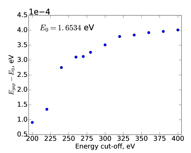
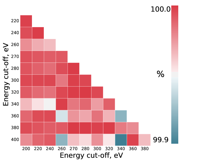
Within chosen cut-off energy limits the band gap changes within 0.02%, a negligibly small value (Fig. S1). The densities of states were compared pairwise. For each pair the Pearson’s correlation coefficientPearson (1895) was calculated. In Fig. S2 the correlation matrix demonstrates a correlation over 99% between different simulations, based on which we can make a conclusion that eDOS is not overly sensitive to varying the energy cut-off.
II Individual electronic spectra for other stoichiometries
III Comparison with electronic spectra obtained in earlier studies
IV Statistics of energy levels
V Comparison of electronic spectra for samples obtained using different values of the threshold parameter
VI Basic properties of the wavefunctions of the topological midgap states, also in the presence of cross-linking with perfectly dimerized chains
To set the stage, we consider an extended, perfectly dimerized chain terminating with the weaker bond on one end, as in Fig. S19(a). In the latter figure, and denote the electronic transfer integrals for the stronger and weaker bond, respectively: . Everywhere below, we assume the on-site energies are equal to zero, for simplicity. The argument can be extended straightforwardly for a non-vanishing, sign-alternating on-site energy. Rice and Mele (1982); Zhugayevych and Lubchenko (2010b) Such a situation would be directly relevant to chain-like motifs in which chalcogen and pnictogen alternate in sequence.

Irrespective of whether the terminal bond is weak or strong, the chain has a bulk spectrum consisting of two bands, the outer edges of the bands at , the band-gap edges at . There is also a midgap, “edge” state for the configuration shown in Fig. S19(a) exactly in the middle of the forbidden gap. To see this, we write down the stationary Schrödinger equation for the components of the wave function, where the subscript labels the sites of the chain:
| (S1) | |||
Clearly, Eqs. (S1) allow for a midgap solution exactly in the middle of the gap:
| (S2) | |||||
The wavefunction vanishes on all even-numbered sites, while on the odd-numbered sites, it alternates in sign while decreasing in magnitude by a factor of per each pair of sites as one moves away from the terminal site. At the latter site, the wavefunction has its largest value. Thus the wave function will decrease exponentially as a function of the distance away from the terminus:
| (S3) |
where is the average spacing between the sites. (We note a peculiar feature of Eq. (S2): If the transfer integral is inversely proportional to the distance between the sites, the wavefunction as a function of the physical coordinate consists of a set of straight lines crossing the origin at the even-numbered sites and thus can be easily drawn by hand, see the dashed line in Fig. S19(a).)
Using the same logic, one can show that such a midgap edge state would not exist if the terminal bond were the strong one because this would entail an exponential increase of the wavefunction toward the bulk of the chain and, consequently, lack of normalizability for the wavefunction. Again, this is straightforwardly evidenced graphically, see the dashed-dotted line in Fig. S19(a).
Non-withstanding their apparent simplicity, Eqs. (S1) demonstrate that the midgap state will persist even if the bond strength varies somewhat in space, as long as the local value of the ratio tends to a steady value less than one in the bulk in the chain. (The latter condition is necessary to have well defined bulk bands in the first place.) The wavefunction will remain zero on the even-numbered sites. To avoid confusion we note that depending on the detailed dependence of the local value of ratio on the coordinate, other midgap states may be present. Takayama et al. (1980)
Now, the above setup can be used to appreciate that the vicinity of an undercoordinated site, in an otherwise perfectly dimerized extended chain, will host a midgap state, as in Fig. S19(b). Hereby, the central site of the defect will correspond to site 1 from Fig. S19(a) while the chain itself and midgap wavefunction to the left of site 1 will be the exact mirror images of the respective entities from the r.h.s. of site 1. Thus the wave function is even with respect to the reflection about the central site and vanishes on sites that a separated by an odd number of bonds from the central site. Likewise, the vicinity of an over-coordinated site will also host a midgap state, as in Fig. S19(c). The center of the defect now corresponds to site 2 from Fig. S19(a). The corresponding wave function is odd with respect to the reflection about the central site; it vanishes on the central site and on sites that are separated by an even number of bonds from the central site. These properties of the midgap states are of course well known, see Ref. Heeger et al., 1988 and references therein. According to those earlier works, if let geometrically optimize, the chain will relax so as to get rid of all midgap states other than the one in the middle, Takayama et al. (1980) which we have seen is robust with respect to vibrational deformations of the chain. This robustness comes about for very general, topological reasons. Heeger et al. (1988)

Next, let us couple a chain containing an under-coordinated center with a perfectly dimerized chain, the corresponding transfer integral set equal to , see Fig. 9 of the main text and Fig. S20. Note that now we number the sites on the chains so that the sites participating in the inter-chain coupling—one of them hosting the defect—are labeled “”. The wave functions on the defected and perfectly dimerized chain are labeled by the letters and , respectively. It will suffice to write out only two entries of the Schrödinger equation
| (S4) | |||
| (S5) |
Eq. (S4) and the rest of the entries pertaining to the defected chain still allow for a midgap solution at , where the wavefunction is an even function vanishing on odd-numbered sites, so long as . Eq. (S5), on the other hand, allows for a solution at such that , , while
| (S6) |
The rest of the positively-numbered ’s obey the same equations as the quantities in Eq. (S2). Clearly, the positively-numbered segment of the dimerized chain is analogous to the setup in Fig. S19(a), since while . The electron occupying the midgap state in the defected chain tunnels within the positively-numbered side of the dimerized chain in the same fashion as the electron occupying the terminal site in Fig. S19(a) tunnels toward the bulk of the chain in that figure. The extent of “spillage” of the midgap state wavefunction from the defected to the defect-free chain will be determined by the strength of the inter-chain coupling, according to Eq. (S6), and could be significant. Physically, the coupling could be realized, for instance, through -mixing, which would involve neighboring atoms and/or if the chains are not strictly perpendicular. In the latter case, the coupling goes roughly , where is the angle between the chains. Finally, similar logic can be used to show that a wavefunction centered on an over-coordinated site will not “spill” into the crossing chain. Indeed, coupling two chains does not change the symmetry of the Hamiltonian with respect to reflection about the respective sites through which the chains are coupled. Thus Eq. (S4) still yields a midgap state at whereby , , and thus . Consequently, if the dimerized chain were to co-host a midgap state, the corresponding wavefunction would have to be an exponential function of the coordinate throughout: , c.f. the bottom equation in (S2). Since such a wavefunction is not normalizable, we conclude that the midgap state based on an over-coordinated site would be confined to the chain along which the malcoordination takes place.
VII Midgap states induced in crystalline slabs
VIII Localization and shape anisotropy of electronic states for samples containing an odd number of electrons