Using controlled disorder to probe the interplay between
charge order and superconductivity in NbSe2
Abstract
The interplay between superconductivity and charge density waves (CDW) in -NbSe2 is not fully understood despite decades of study. Artificially introduced disorder can tip the delicate balance between two competing forms of long-range order, and reveal the underlying interactions that give rise to them. Here we introduce disorders by electron irradiation and measure in-plane resistivity, Hall resistivity, X-ray scattering, and London penetration depth. With increasing disorder, varies nonmonotonically, whereas monotonically decreases and becomes unresolvable above a critical irradiation dose where drops sharply. Our results imply that CDW order initially competes with superconductivity, but eventually assists it. We argue that at the transition where the long-range CDW order disappears, the cooperation with superconductivity is dramatically suppressed. X-ray scattering and Hall resistivity measurements reveal that the short-range CDW survives above the transition. Superconductivity persists to much higher dose levels, consistent with fully gapped superconductivity and moderate interband pairing.
The interplay between superconductivity (SC) and density wave orders has been a central issue in high temperature superconductors such as cuprates and iron-based superconductors Dai (2015). The recent discovery of a charge density wave (CDW) phase in the middle of the pseudogap region of cuprates Ghiringhelli et al. (2012); Chang et al. (2012); Achkar et al. (2012); Comin et al. (2014); da Silva Neto et al. (2014); Tabis et al. (2014) has revitalized interest in the interplay between CDW and superconducting states in other unconventional superconductors, such as the layered transition-metal dichalcogenides, in particular well-studied 2-NbSe2 Gabovich et al. (2001); Wilson et al. (1975); Moncton et al. (1975); Harper et al. (1975). This system has fascinated investigators for decades due to microscopic coexistence of CDW ( K) and SC ( K) states Guillamon et al. (2008); Sooryakumar and Klein (1980). The coupling between the two long-range orders is apparently responsible for the observability of the elusive Higgs bosonic amplitude mode of the superconductor Littlewood and Varma (1981, 1982), discovered by Raman scattering on 2-NbSe2 Méasson et al. (2014); Grasset et al. (2018).
Despite intense effort, however, a key question regarding the nature of the coupling of the two orders in this system is still under debate. In recent years, the conventional weak-coupling picture where CDW and SC compete for parts of the Fermi surface has been challenged by the realization that the electron-phonon coupling is very strong due to the two-dimensional confinement of the Nb layer Moncton et al. (1975); Inglesfield (1980); Varma and Simons (1983); Weber et al. (2011); Flicker and van Wezel (2015). In such a situation, the usual mean field picture of a charge density wave order with rigid amplitude and phase disappearing at may no longer be valid, since the short-range CDW order together with a gap in the electronic spectrum have been observed outside the long-range ordered phase Chatterjee et al. (2015).
The situation in 2-NbSe2 is complicated by the complex electronic bandstructure of this material and apparent multiband superconductivity with two effective gaps Fletcher et al. (2007). Different superconducting gaps on different Fermi surface sheets were inferred from angle-resolved photoemission spectroscopy (ARPES) by Yokoya et al. Yokoya et al. (2001) and thermal conductivity measurements by Boaknin et al. Boaknin et al. (2003). Kiss et al. proposed that the CDW actually boosts the superconductivity, based on the correlation with the largest electron-phonon coupling and lowest Fermi velocities at the same -points Kiss et al. (2007). Borisenko et al. observed Fermi arcs, suggesting that the CDW inhibits the formation of superconducting order by gapping the nested portion of Fermi surface Borisenko et al. (2009).
The pressure dependence of and is another way to study the interplay between the CDW and superconductivity. Leroux et al. suggest that the pressure and temperature dependence of the phonon dispersion, observed by inelastic X-ray scattering, support insensitivity of to the CDW transition Leroux et al. (2015). However, Feng et al. reported a broad regime of order parameter fluctuations in X-ray diffraction (at = 3.5 K), and attributed it to the presence of a CDW quantum critical point (PCDW = 4.6 GPa) buried beneath the superconducting dome Feng et al. (2012). They also claimed that this is partially consistent with the increasing under pressure up to about 4.6 GPa Berthier et al. (1976). Suderow et al. proposed a peculiar interplay among superconductivity, CDW order, and Fermi surface complexity, based on the mismatch between the suppression of at 5 GPa and the maximum at 10.5 GPa Suderow et al. (2005). Chatterjee et al. Chatterjee et al. (2015) studied the effect of transition metal doping on the CDW state using ARPES, X-ray diffraction, STM tunneling, and resistivity, and showed that short range CDW order and an energy gap remained at high temperatures and high disorder beyond the phase coherence transition.
Another way to probe CDW and SC states is to introduce non-magnetic point-like scatterersMutka (1983); Grest et al. (1982); Hirschfeld and Goldenfeld (1993); Wang et al. (2013); Cho et al. (2016). Electron irradiation, which has been shown to create pure atomic disorder without doping the system as deduced from Hall effect measurements, is an effective tool to influence both the superconductivity and other orders Prozorov et al. (2014, ); Cho et al. (2018). Moreover, independent measurements of , and low-temperature London penetration depth in samples with controlled disorder become powerful techniques that can distinguish different types of superconducting pairing such as wave, , and pairing Hirschfeld and Goldenfeld (1993); Efremov et al. (2011); Wang et al. (2013). Indeed, this approach was successfully used in various iron-based superconductors Prozorov et al. (2014); Mizukami et al. (2014); Strehlow et al. (2014); Cho et al. (2016). According to early studies of the effect of electron irradiation on NbSe2 by Mutka et al. Mutka (1983), an increase of was reported but attributed to inhomogeneous superconductivity. This result was theoretically discussed by Grest et al. Grest et al. (1982) and Psaltakis et al., Psaltakis (1984), but direct evidence determining the effect of homogeneously distributed disorder on the interplay between the CDW and SC states is still missing.
In this article, we systematically investigate the effect of controlled point-like disorder on superconductivity and CDW order in 2-NbSe2. The disorder is generated by applying 2.5 MeV electron irradiation with different doses. For each dose, the changes in , residual resistivity, Hall coefficient, and London penetration depth are measured. For low irradiation doses, shows nonmonotonic behavior, first increasing slightly and then decreasing until a critical dose of 1.0 C cm-2 where it drops abruptly. At this critical dose, the long-range CDW feature in resistivity disappears as well. The vanishing of appears to be discontinuous. Upon further irradiation, we find the existence of persistent short-range CDW correlations based on X-ray scattering and Hall resistivity measurements, and attribute the abrupt drop in to the loss of coherence of the phase-coherent CDW order. Among various possible mechanisms, we conclude that the effect of the reconstruction of the electronic structure by the CDW leads to a rapid change of electron-phonon scattering at the critical dose of 1.0 C cm-2, explaining a remarkable qualitative change in the Hall effect and an abrupt drop of . This represents a clear evidence for a special role of the coherent CDW state coupling to superconductivity. Furthermore, the change in provides important information on the nature of the pairing both within and outside of the long-range CDW state. Upon irradiation above the critical dose, continuously decreases down to the largest dose applied, suggesting a substantial degree of gap anisotropy. The low temperature London penetration depths of three post-irradiated samples consistently show exponentially saturating behavior below 0.2 , with gaps that increase with disorder and are therefore consistent with this picture.
I Results
I.1 Effect of electron irradiation on resistivities
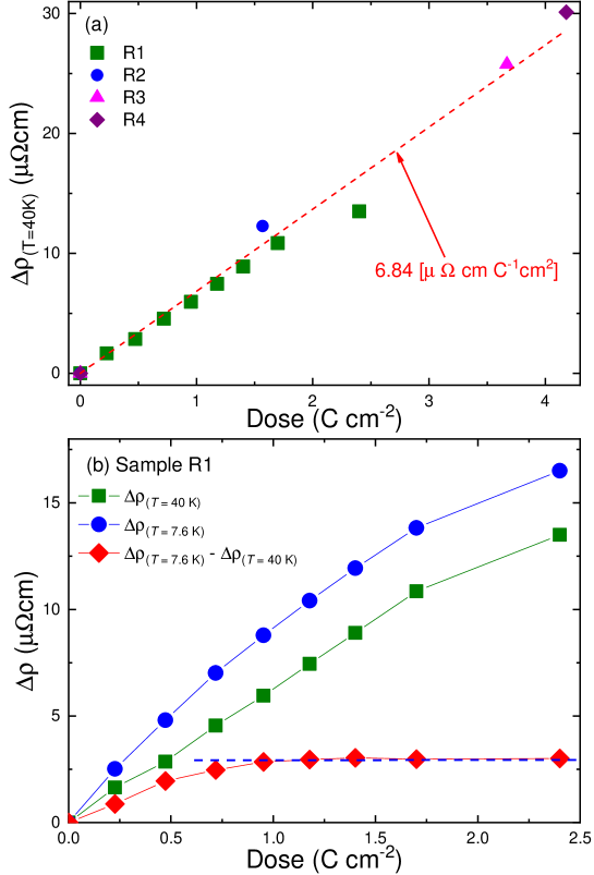
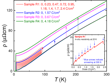
Electron irradiation (maximum dose of 8.93 C cm-2) effectively introduces artificial disorder into the system, resulting in the substantial increase of residual resistivity in the normal state, as shown in Fig. 1. Above 40 K without long-range CDW order, the increase of resistivity is rather constant. However, near and below 40 K, a violation of Matthiesen’s rule was observed due to the presence of the CDW phase. For cases with high doses of irradiation ( 1.0 C cm-2) where the CDW feature in resistivity was completely suppressed due to disorder, Matthiesen’s rule was obeyed over the entire temperature region of the normal state. To investigate how effectively the electron irradiation introduces defects, the in-situ resistivity of sample R1 was measured during the irradiation at 22 K (inset of Fig. 1). It increases monotonically with increasing dose of irradiation. The blue arrows indicate when the irradiation stopped and room temperature annealing occurred. About 30 - 40 annealing occurred for each case. For each dose (blue arrow), the sample was removed from the irradiation chamber and moved to a different cryostat for measurement of the temperature dependent resistivity as shown in Fig. 1 and 2 (b).
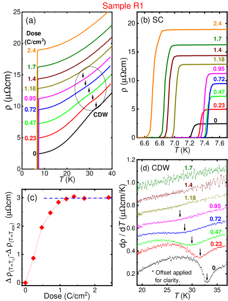
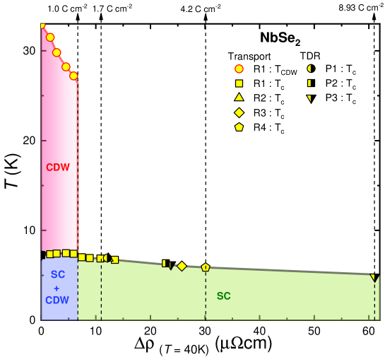
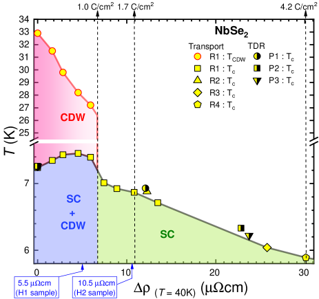
With increasing irradiation dose, both the superconducting and CDW phases were substantially affected. As shown in Fig. 2 (a), (kink feature marked by arrow) decreases with increasing irradiation and disappears after 1.0 C cm-2. The behavior of the CDW feature is more clearly shown in a plot of versus temperature (Fig. 2 (d)). The important fact is that the feature associated with the CDW transition disappears at finite temperature of 27 K instead of continuing down to zero Kelvin. This result suggests the absence of a quantum critical point with disorder, in contrast to the previous pressure study by Feng et al.. Feng et al. (2012). Fig. 2 (b) is an enlargement of the low-temperature part of Fig. 2 (a) that shows the change of . It is clearly seen that initially increases and then decreases upon irradiation. All the values of and for sample R1 are summarized in Fig. 4 along with ’s from other samples (R2, R3, R4, P1, P2, P3). The -axis of Fig. 4 is the increase of resistivity at 40 K, , upon irradiation (representing increased disorder). With increasing dose of irradiation up to 1.0 C cm-2 ( = 7.3 cm), gradually increases from 7.25 K to 7.45 K, and then starts decreasing back to 7.3 K while monotonically decreases. Upon further irradiation, the feature associated with the CDW transition disappears and simultaneously abruptly drops by 0.3 K, indicating strong correlation between the superconducting and CDW phases. Note the mismatch between the maximum and the disappearance of the CDW feature, suggesting a complex interplay between the two phases potentially including other factors such as complicated Fermi surfaces. Upon further irradiation, continues to decrease toward about 33 of its pristine value for the maximum electron dose of 8.93 C cm-2 ( = 61 cm) as shown in the full phase diagram in Supplementary Figure 1.
I.2 Effect of electron irradiation on the London penetration depth
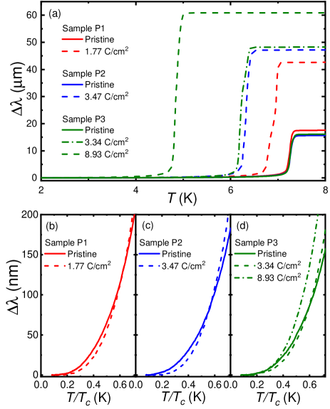
Fig. 3 exhibits the temperature dependence of the London penetration depth () of P1, P2 and P3 samples upon irradiation. The low temperature saturation is clearly seen below 0.2 / for all samples before and after irradiation, suggesting the presence of s-wave type superconducting gaps. Interestingly, the saturation tendency gets stronger after irradiation, suggesting that the initial anisotropic gaps get more isotropic due to the gap-smearing effect of point-like disorder. Note that the irradiation doses shown correspond to residual resistivities beyond the initial enhancement of due to competition with the CDW phase, so that a uniform enhancement of is not the main cause of the saturation in . In addition, a substantial decrease of from 7.25 K to 4.8 K (about 33 decrease) was found in sample P3 upon 8.93 C cm-2. All the suppressions from these three samples (P1, P2, P3) are summarized in Fig. 4. Since we cannot directly obtain for P1, P2, and P3, we used the relation between dose and obtained from transport-measured samples (R1, R2, R3, and R4) as shown in Supplementary Figure 2 (a). The substantial decrease of and exponential-like saturation of can be explained with multiband s-wave type superconducting gap with some amount of interband coupling.
I.3 Phase diagram upon electron irradiation
Fig. 4 shows the temperature versus phase diagram of superconductivity and charge density wave upon electron irradiation obtained from seven samples. Upon initial irradiation up to 1.0 C cm-2, an anticorrelation of and was observed, which is most naturally interpreted in terms of strong competition between the superconducting and CDW phases. However, after reaches its maximum, both and decrease until the CDW phase abruptly disappears at a critical irradiation dose of 1.0 C cm-2, where also drops discontinuously. The simplest explanation of the nonmonotonic behavior of in the CDW coexistence phase is that the initial increase is due to the competition between the superconductivity and CDW phases. The effect of disorder on this competition was studied already by Grest et al. Grest et al. (1982) and Psaltakis et al. Psaltakis (1984). Within this weak-coupling approach, non-magnetic disorder suppresses the CDW rapidly, and since the CDW order is competing for Fermi surface with superconductivity, increases. Note that these theoretical calculations assumed an isotropic -wave gap; within their approximations, the superconducting would have saturated when CDW order vanished, due to Anderson’s theorem. However, it is clear from Fig. 4 that disorder continues to suppress long after the CDW order is gone; this implies that the -wave gaps have quite different amplitudes (and, possibly, anisotropy) and substantial interband pairing. Furthermore, as will be shown in Figs. 5 and 6, we found from the Hall resistivity and X-ray scattering that the short-range CDW phase still survives long after the critical dose of 1.0 C cm-2.
I.4 X-ray diffraction upon electron irradiation
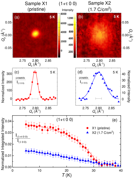
Figure 5 shows the characterization of the CDW of samples X1 (pristine) and X2 (1.7 C cm-2) by high-energy x-ray diffraction. The structure of NbSe2 consists of layers of Nb atoms surrounded by 6 Se atoms and the Nb atoms located in the corners of the hexagonal unit cell Marezio et al. (1972). The CDW displaces the six nearest Nb neighbors of every third Nb atom, yielding a superstructure with tripling of the unit-cell dimensions in both a and b directions, and corresponding propagation vectors ( 0 0) and (0 0) with = 1/3 Malliakas and Kanatzidis (2013). For both samples, the CDW Bragg peaks are observed in all measured Brillouin zones at low temperature. The CDW Bragg peaks are resolution limited, as illustrated in Figs. 5 (a) and (c) for sample X1, whereas they show a significant broadening in panels (b) and (d) for sample X2 which is temperature-independent. Note that the intensity scales in panels (a) and (c) are about seven times larger than those in panel (b) and (d). From the peak widths determined by Gaussian fits to the cuts shown in Figs. 5 (c) and (d), the correlation length of the CDW is estimated to be about 80 Å for the irradiated sample X2 and a lower limit of 200 Å for the pristine sample X1. The temperature dependence of the normalized integrated CDW Bragg peak intensity shown in Fig. 5 (e) represents the square of the CDW order parameter and is clearly consistent with a second-order phase transition at = 33 K and long-range order for sample X1. In contrast, the CDW intensity of the irradiated sample X2 increases continuously with decreasing temperature without a clear onset, indicating a cross-over like behavior. Together with the reduced correlation length, it is clear that the CDW manifests only short-range order in the irradiated sample X2, although the strength of the CDW is almost similar to the pristine sample X1 with the integrated Bragg peak intensity only reduced by 65 % at low temperature.
The CDW appears in the same manner with comparable strength in irradiated samples but with a reduced correlation length. The irradiation induced defects likely form barriers or pinning centers for boundaries of the CDW state and prevent a coherently ordered state beyond these defects when the CDW state develops with decreasing temperature. The crossover-like temperature dependence of the short-range CDW without a clear onset observed for the sample X2 is consistent with the lack of a well-defined feature or signature of the CDW in transport measurements for samples with radiation levels above the critical dose of 1.0 C cm-2.
I.5 Hall resistivities upon electron irradiation
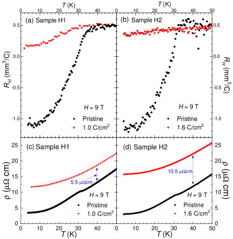
Hall resistivities were measured for samples H1 and H2 as shown in Fig. 6 (a) and (b). For sample H1, two measurements were conducted before and after irradiation with 1.0 C cm-2, and for sample H2, before and after irradiation with 1.6 C cm-2. First of all, the Hall resistivity of both pristine samples shows a sign-change below = 33 K, consistent with previous reports Yamaya and Sambongi (1972); Bel et al. (2003). This indicates an increase of mobility in the CDW phase, consistent with previous reports in resistivity and Nernst effect Bel et al. (2003), due to an opening of the pseudogap Evtushinsky et al. (2008). The change of in-plane resistivity, , as shown in in panels (c) and (d), was used to accurately calibrate the amount of disorder, yielding = 5.5 cm for sample H1 and 10.5 cm for H2. These values allow us to place the samples before and after the critical transition, respectively, as shown in the phase diagram (blue arrows in -axis) of Fig. 4. The CDW transition is clearly seen for sample H1 in Fig. 6 (a), consistent with the observation of a feature in the resistivity derivative. For sample H2, however, the feature at the CDW transition almost disappears in Fig. 6 (b) although a slight slope change can be noticed at 30 K. This is consistent with the disappearance of the long - range CDW feature (resistivity) and the presence of a short -range CDW (X-ray scattering) above the critical dose. Another important fact is that the Hall resistivity above 40 K did not change upon irradiation. This implies that the defects introduced by electron irradiation do not change the electronic carrier density above 40 K, but only increase the scattering rate.
II Discussion
Evidence for an anisotropic superconducting gap in NbSe2 is provided, e.g. by STM measurements, which show a significantly broadened gap edge Guillamon et al. (2008). In addition, the flattening of the low- penetration depth upon irradiation at doses corresponding to the pure superconducting phase is evident in Fig. 3. Since the smallest gap in the system will determine the asymptotic low- exponential dependence, it suggests that disorder is increasing the minimum gap, i.e. gap averaging. The nonmonotonic behavior of in the CDW/SC coexistence phase can therefore be understood simply by assuming that the effect of losing competition from the CDW is overcome by the gap averaging effect before the CDW disappears. It should be noted, however, that the behavior with pressure is also nonmonotonic Suderow et al. (2005) In this case the reason for the continued suppression of is less obvious, and the pressure dependence of the couplings of various phonons may be necessary to explain the complete behavior quantitatively.
The possibility of a first-order transition at the disappearance of CDW order is also intriguing and recalls the question of the CDW mechanism. A simple Fermi surface nesting model Wilson (1977) fails to explain the CDW ordering vector, and is therefore not appropriate for NbSe2Valla et al. (2004); Weber et al. (2011). Similarly, a saddle point-driven CDW instability proposed by Rice and Scott Rice and Scott (1975) has been ruled out by ARPES Rossnagel et al. (2001). However, a generalized Fermi surface nesting model, which includes the strong anisotropy in the electron-phonon matrix elements, does capture the correct CDW ordering vector Doran (1978); Flicker and van Wezel (2015). The generalized Fermi-surface nesting model is still effectively a weak coupling model, where a strong momentum dependence of the electron-phonon matrix elements modifies the peak position of the charge susceptibility. Hence, from a weak coupling perspective, a disorder-driven first order transition, as apparently observed here, appears to be a natural one. This is because the CDW is a Stoner-type instability, where with increasing disorder the charge susceptibility at ordering vectors should drop below a critical value corresponding to ordering.
Observation of a quantum critical point under pressure might be taken as evidence against the idea of first order transitionFeng et al. (2012). However, one should keep in mind that pressure also changes the bare electronic structure, which does not happen in case of point like impurities. Disorder is often thought to drive a first order transition, e.g. in the manganites Dagotto (2005). We note that Chatterjee et al. Chatterjee et al. (2015) deduced a smooth decay of CDW order with chemical substitution, but in fact their data are entirely consistent with ours because of the relatively small number of doping levels studied in that work.
We cannot definitively rule out the possibility that the feature observed in transport, here identified as the signature of long-range CDW order, simply becomes too weak to observe because of broadening due to significant short-range fluctuations, as observed in Ref. Chatterjee et al., 2015. However, our new observation of a concomitant abrupt drop in suggests that a thermodynamic transition is indeed taking place at this critical value of disorder. Unlike incommensurate CDW systems, commensurate CDW transitions as in NbSe2 in the presence of quenched disorder may occur Nie et al. (2014). The ordered phase in such a situation breaks translational symmetry discretely, so that a second order transition with exponents dependent on the order of the commensurability is allowed, but this can be preempted by a first order transition, as apparently observed here.
We investigated the interplay between the CDW and superconducting phases in 2-NbSe2 by measuring the resistivity and penetration depth before and after electron irradiation. Upon initial irradiation, increased from 7.25 K to 7.45 K, and then decreased while monotonically decreased. This indicates a complex interplay between two phases with potential other factor such as a complicated Fermi surface. Upon further irradiation, the feature associated with the CDW transition disappeared at finite temperature. When the CDW feature disappears, abruptly dropped by 0.2 K, indicating strong correlation between two phases and suggesting a first order, disorder driven phase transition. Further irradiation up to 8.93 C cm-2 effectively and monotonically decreased down to 4.8 K (about 33 of its pristine value), suggestive of the averaging of an anisotropic -wave superconducting order parameter. According to X- ray scattering and Hall resistivity studies, the short-range CDW is still present after the critical dose of 1.0 C cm-2 ( 7.3 cm) indicating that the effect of electron irradiation decreases the coherence of the CDW phase. The low-temperature penetration depth shows exponential-like behavior below 0.2 / for all samples before and after irradiation. The combined results of resistivity and penetration depth can be explained with multiband anisotropic s-wave type superconducting gaps with some amount of interband coupling.
III Methods
III.1 Crystal growth
The single crystals of 2-NbSe2 from Bell Laboratories were grown using the usual iodine vapor transport technique and are known to be of high quality (RRR 40). These are the samples from the same batch as used in Ref. Fletcher et al. (2007). Four-probe measurements of in-plane resistivity were performed for four samples (R1, R2, R3, and R4). Samples for resistivity measurements had dimensions of (1-2) 0.5 (0.02-0.1) mm3. Electrical contacts to samples prior to irradiation were made by soldering 50-m silver wires with indium and mechanically strengthened by silver paste as described elsewhere Tanatar et al. (2016). For in-situ resistivity measurement during the electron-irradiation at 22 K, R1 sample was mounted on a Kyocera chip as shown in the inset of Fig. 1 and measured during irradiation.
III.2 Resistivity measurements
Simultaneous Hall effect and resistivity measurements were performed on samples H1 and H2 mounted in 5-probe configuration using the same contact making technique as in resistivity measurements. Measurements were taken in Quantum Design PPMS in constant magnetic fields +9T and -9T. Same samples with the same contacts were measured before and after irradiation, thus excluding geometric factor errors in quantitative comparison.
III.3 London penetration depth
The in-plane London penetration depth (T) of three other samples (P1, P2, and P3) was measured before and after irradiation using a self-oscillating tunnel-diode resonator technique Prozorov et al. (2000); Prozorov and Giannetta (2006); Prozorov and Kogan (2011). The samples had typical dimensions of 0.5 0.5 0.03 mm3.
III.4 X-ray diffraction
The high-energy x-ray diffraction study was performed at station 6-ID-D at the Advanced Photon Source, Argonne National Laboratory. The use of x-rays with an energy of 100.5 keV minimizes sample absorption and allows to probe the entire bulk of the sample using an incident beam with a size of 0.5 0.5 mm2, over-illuminating the sample. The samples were held on Kapton tape in a Helium closed-cycle refrigerator and Helium exchange gas was used. Extended regions of selected reciprocal lattice planes were recorded by a MAR345 image plate system positioned 1468 mm behind the sample as the sample was rocked through two independent angles up to about axes perpendicular to the incident beam Kreyssig et al. (2007).
III.5 Electron irradiation
The 2.5 MeV electron irradiation was performed at the SIRIUS Pelletron facility of the Laboratoire des Solides Irradies (LSI) at the Ecole Polytechnique in Palaiseau, France van der Beek et al. (2013). The acquired irradiation dose is conveniently measured in C cm-2, where 1 C cm-2 = 6.24 1018 electrons/cm2.
III.6 Data availability
The authors declare that all data supporting the findings of this study are available within the article and its supplementary information files or from the corresponding author upon reasonable request.
References
- Dai (2015) P. Dai, Reviews of Modern Physics 87, 855 (2015).
- Ghiringhelli et al. (2012) G. Ghiringhelli, M. Le Tacon, M. Minola, S. Blanco-Canosa, C. Mazzoli, N. B. Brookes, G. M. De Luca, A. Frano, D. G. Hawthorn, F. He, T. Loew, M. M. Sala, D. C. Peets, M. Salluzzo, E. Schierle, R. Sutarto, G. A. Sawatzky, E. Weschke, B. Keimer, and L. Braicovich, Science 337, 821 (2012).
- Chang et al. (2012) J. Chang, E. Blackburn, A. T. Holmes, N. B. Christensen, J. Larsen, J. Mesot, R. Liang, D. A. Bonn, W. N. Hardy, A. Watenphul, M. v. Zimmermann, E. M. Forgan, and S. M. Hayden, Nature Physics 8, 871 (2012).
- Achkar et al. (2012) A. J. Achkar, R. Sutarto, X. Mao, F. He, A. Frano, S. Blanco-Canosa, M. Le Tacon, G. Ghiringhelli, L. Braicovich, M. Minola, M. Moretti Sala, C. Mazzoli, R. Liang, D. A. Bonn, W. N. Hardy, B. Keimer, G. A. Sawatzky, and D. G. Hawthorn, Physical Review Letters 109, 167001 (2012).
- Comin et al. (2014) R. Comin, A. Frano, M. M. Yee, Y. Yoshida, H. Eisaki, E. Schierle, E. Weschke, R. Sutarto, F. He, A. Soumyanarayanan, Y. He, M. Le Tacon, I. S. Elfimov, J. E. Hoffman, G. A. Sawatzky, B. Keimer, and A. Damascelli, Science 343, 390 (2014).
- da Silva Neto et al. (2014) E. H. da Silva Neto, P. Aynajian, A. Frano, R. Comin, E. Schierle, E. Weschke, A. Gyenis, J. Wen, J. Schneeloch, Z. Xu, S. Ono, G. Gu, M. Le Tacon, and A. Yazdani, Science 343, 393 (2014).
- Tabis et al. (2014) W. Tabis, Y. Li, M. L. Tacon, L. Braicovich, A. Kreyssig, M. Minola, G. Dellea, E. Weschke, M. J. Veit, M. Ramazanoglu, A. I. Goldman, T. Schmitt, G. Ghiringhelli, N. Barišić, M. K. Chan, C. J. Dorow, G. Yu, X. Zhao, B. Keimer, and M. Greven, Nature Communications 5, 5875 (2014).
- Gabovich et al. (2001) A. M. Gabovich, A. I. Voitenko, J. F. Annett, and M. Ausloos, Superconductor Science and Technology 14, R1 (2001).
- Wilson et al. (1975) J. Wilson, F. D. Salvo, and S. Mahajan, Advances in Physics 24, 117 (1975).
- Moncton et al. (1975) D. E. Moncton, J. D. Axe, and F. J. DiSalvo, Physical Review Letters 34, 734 (1975).
- Harper et al. (1975) J. Harper, T. Geballe, and F. D. Salvo, Physics Letters A 54, 27 (1975).
- Guillamon et al. (2008) I. Guillamon, H. Suderow, F. Guinea, and S. Vieira, Physical Review B 77, 134505 (2008).
- Sooryakumar and Klein (1980) R. Sooryakumar and M. V. Klein, Physical Review Letters 45, 660 (1980).
- Littlewood and Varma (1981) P. B. Littlewood and C. M. Varma, Physical Review Letters 47, 811 (1981).
- Littlewood and Varma (1982) P. B. Littlewood and C. M. Varma, Physical Review B 26, 4883 (1982).
- Méasson et al. (2014) M.-A. Méasson, Y. Gallais, M. Cazayous, B. Clair, P. Rodière, L. Cario, and A. Sacuto, Physical Review B 89, 060503 (2014).
- Grasset et al. (2018) R. Grasset, T. Cea, Y. Gallais, M. Cazayous, A. Sacuto, L. Cario, L. Benfatto, and M.-A. Méasson, Physical Review B 97, 094502 (2018).
- Inglesfield (1980) J. E. Inglesfield, Journal of Physics C: Solid State Physics 13, 17 (1980).
- Varma and Simons (1983) C. M. Varma and A. L. Simons, Physical Review Letters 51, 138 (1983).
- Weber et al. (2011) F. Weber, S. Rosenkranz, J.-P. Castellan, R. Osborn, R. Hott, R. Heid, K.-P. Bohnen, T. Egami, A. H. Said, and D. Reznik, Physical Review Letters 107, 107403 (2011).
- Flicker and van Wezel (2015) F. Flicker and J. van Wezel, Nature Communications 6, 7034 (2015).
- Chatterjee et al. (2015) U. Chatterjee, J. Zhao, M. Iavarone, R. di Capua, J. P. Castellan, G. Karapetrov, C. D. Malliakas, M. G. Kanatzidis, H. Claus, J. P. C. Ruff, F. Weber, J. van Wezel, J. C. Campuzano, R. Osborn, M. Randeria, N. Trivedi, M. R. Norman, and S. Rosenkranz, Nature Communications 6, 6313 (2015).
- Fletcher et al. (2007) J. D. Fletcher, A. Carrington, P. Diener, P. Rodière, J. P. Brison, R. Prozorov, T. Olheiser, and R. W. Giannetta, Physical Review Letters 98, 057003 (2007).
- Yokoya et al. (2001) T. Yokoya, T. Kiss, A. Chainani, S. Shin, M. Nohara, and H. Takagi, Science 294, 2518 (2001).
- Boaknin et al. (2003) E. Boaknin, M. A. Tanatar, J. Paglione, D. Hawthorn, F. Ronning, R. W. Hill, M. Sutherland, L. Taillefer, J. Sonier, S. M. Hayden, and J. W. Brill, Physical Review Letters 90, 117003 (2003).
- Kiss et al. (2007) T. Kiss, T. Yokoya, A. Chainani, S. Shin, T. Hanaguri, M. Nohara, and H. Takagi, Nature Physics 3, 720 (2007).
- Borisenko et al. (2009) S. V. Borisenko, A. A. Kordyuk, V. B. Zabolotnyy, D. S. Inosov, D. Evtushinsky, B. Büchner, A. N. Yaresko, A. Varykhalov, R. Follath, W. Eberhardt, L. Patthey, and H. Berger, Physical Review Letters 102, 166402 (2009).
- Leroux et al. (2015) M. Leroux, I. Errea, M. Le Tacon, S.-M. Souliou, G. Garbarino, L. Cario, A. Bosak, F. Mauri, M. Calandra, and P. Rodière, Physical Review B 92, 140303 (2015).
- Feng et al. (2012) Y. Feng, J. Wang, R. Jaramillo, J. van Wezel, S. Haravifard, G. Srajer, Y. Liu, Z.-A. Xu, P. B. Littlewood, and T. F. Rosenbaum, Proceedings of the National Academy of Sciences 109, 7224 (2012).
- Berthier et al. (1976) C. Berthier, P. Molinié, and D. Jérome, Solid State Communications 18, 1393 (1976).
- Suderow et al. (2005) H. Suderow, V. G. Tissen, J. P. Brison, J. L. Martínez, and S. Vieira, Physical Review Letters 95, 117006 (2005).
- Mutka (1983) H. Mutka, Physical Review B 28, 2855 (1983).
- Grest et al. (1982) G. S. Grest, K. Levin, and M. J. Nass, Physical Review B 25, 4562 (1982).
- Hirschfeld and Goldenfeld (1993) P. J. Hirschfeld and N. Goldenfeld, Physical Review B 48, 4219 (1993).
- Wang et al. (2013) Y. Wang, A. Kreisel, P. J. Hirschfeld, and V. Mishra, Physical Review B 87, 094504 (2013).
- Cho et al. (2016) K. Cho, M. Kończykowski, S. Teknowijoyo, M. A. Tanatar, Y. Liu, T. A. Lograsso, W. E. Straszheim, V. Mishra, S. Maiti, P. J. Hirschfeld, and R. Prozorov, Science Advances 2, e1600807 (2016).
- Prozorov et al. (2014) R. Prozorov, M. Kończykowski, M. A. Tanatar, A. Thaler, S. L. Bud’ko, P. C. Canfield, V. Mishra, and P. J. Hirschfeld, Physical Review X 4, 041032 (2014).
- (38) R. Prozorov, M. Konczykowski, M. A. Tanatar, B. Shen, H. H. Wen, I. I. Mazin, and R. M. Fernandes, unpublished .
- Cho et al. (2018) K. Cho, M. Kończykowski, S. Teknowijoyo, M. A. Tanatar, and R. Prozorov, Superconductor Science and Technology 31, 064002 (2018).
- Efremov et al. (2011) D. V. Efremov, M. M. Korshunov, O. V. Dolgov, A. A. Golubov, and P. J. Hirschfeld, Physical Review B 84, 180512 (2011).
- Mizukami et al. (2014) Y. Mizukami, Y. Kończykowski, M. andKawamoto, S. Kurata, S. andKasahara, K. Hashimoto, V. Mishra, Y. Kreisel, A. andWang, P. J. Hirschfeld, Y. Matsuda, and T. Shibauchi, Nat. Comm. 5, 5657 (2014).
- Strehlow et al. (2014) C. P. Strehlow, M. Kończykowski, J. A. Murphy, S. Teknowijoyo, K. Cho, M. A. Tanatar, T. Kobayashi, S. Miyasaka, S. Tajima, and R. Prozorov, Physical Review B 90, 020508 (2014).
- Psaltakis (1984) G. C. Psaltakis, Journal of Physics C: Solid State Physics 17, 2145 (1984).
- Marezio et al. (1972) M. Marezio, P. Dernier, A. Menth, and G. Hull, Journal of Solid State Chemistry 4, 425 (1972).
- Malliakas and Kanatzidis (2013) C. D. Malliakas and M. G. Kanatzidis, Journal of the American Chemical Society 135, 1719 (2013).
- Yamaya and Sambongi (1972) K. Yamaya and T. Sambongi, Solid State Communications 11, 903 (1972).
- Bel et al. (2003) R. Bel, K. Behnia, and H. Berger, Physical Review Letters 91, 066602 (2003).
- Evtushinsky et al. (2008) D. V. Evtushinsky, A. A. Kordyuk, V. B. Zabolotnyy, D. S. Inosov, B. Büchner, H. Berger, L. Patthey, R. Follath, and S. V. Borisenko, Physical Review Letters 100, 236402 (2008).
- Wilson (1977) J. A. Wilson, Physical Review B 15, 5748 (1977).
- Valla et al. (2004) T. Valla, A. V. Fedorov, P. D. Johnson, P.-A. Glans, C. McGuinness, K. E. Smith, E. Y. Andrei, and H. Berger, Physical Review Letters 92, 086401 (2004).
- Rice and Scott (1975) T. M. Rice and G. K. Scott, Physical Review Letters 35, 120 (1975).
- Rossnagel et al. (2001) K. Rossnagel, O. Seifarth, L. Kipp, M. Skibowski, D. Voß, P. Krüger, A. Mazur, and J. Pollmann, Physical Review B 64, 235119 (2001).
- Doran (1978) N. J. Doran, Journal of Physics C: Solid State Physics 11, L959 (1978).
- Dagotto (2005) E. Dagotto, Science 309, 257 (2005).
- Nie et al. (2014) L. Nie, G. Tarjus, and S. A. Kivelson, Proceedings of the National Academy of Sciences 111, 7980 (2014).
- Tanatar et al. (2016) M. A. Tanatar, A. E. Böhmer, E. I. Timmons, M. Schütt, G. Drachuck, V. Taufour, K. Kothapalli, A. Kreyssig, S. L. Bud’ko, P. C. Canfield, R. M. Fernandes, and R. Prozorov, Physical Review Letters 117, 127001 (2016).
- Prozorov et al. (2000) R. Prozorov, R. W. Giannetta, A. Carrington, and F. M. Araujo-Moreira, Physical Review B 62, 115 (2000).
- Prozorov and Giannetta (2006) R. Prozorov and R. W. Giannetta, Superconductor Science and Technology 19, R41 (2006).
- Prozorov and Kogan (2011) R. Prozorov and V. G. Kogan, Reports on Progress in Physics 74, 124505 (2011).
- Kreyssig et al. (2007) A. Kreyssig, S. Chang, Y. Janssen, J. W. Kim, S. Nandi, J. Q. Yan, L. Tan, R. J. McQueeney, P. C. Canfield, and A. I. Goldman, Physical Review B 76, 054421 (2007).
- van der Beek et al. (2013) C. J. van der Beek, S. Demirdis, D. Colson, F. Rullier-Albenque, Y. Fasano, T. Shibauchi, Y. Matsuda, S. Kasahara, P. Gierlowski, and M. Konczykowski, Journal of Physics: Conference Series 449, 012023 (2013).
Acknowledgements
The authors are grateful to H. Suderow, S. Raghu, S. Sachdev, and R. J. Cava for useful discussions. The work in Ames Laboratory was supported by the U.S. Department of Energy (DOE), Office of Science, Basic Energy Sciences, Materials Science and Engineering Division. Ames Laboratory is operated for the U.S. DOE by Iowa State University under contract DE-AC02-07CH11358. P.J.H. was supported by NSF Grant No. DMR-1407502. We thank the SIRIUS team, O. Cavani and B. Boizot, for operating electron irradiation SIRIUS facility at École Polytechnique [supported by the EMIR (Réseau national d’accélérateurs pour les Études des Matériaux sous Irradiation) network, proposal 15-5788]. We thank Bing Li, W. R. Meier, and D. S. Robinson for experimental support of the x-ray diffraction study. The x-ray study used resources of the Advanced Photon Source, a U.S. Department of Energy (DOE) Office of Science User Facility operated for the DOE Office of Science by Argonne National Laboratory under Contract No. DE-AC02-06CH11357.
IV Supplementary information
This article is published in Nature Communications 9, 2786 (2018). https://doi.org/10.1038/s41467-018-05153-0.