Solution Monolayer Epitaxy for Tunable Atomically Sharp Oxide Interfaces
Abstract
Epitaxial growth of atomically-sharp interfaces serves as one of the main building blocks of nanofabrication. Such interfaces are crucial for the operation of various devices including transistors, photo-voltaic cells, and memory components. In order to avoid charge traps that may hamper the operation of such devices, it is critical for the layers to be atomically-sharp. Fabrication of atomically sharp interfaces normally requires ultra-high vacuum techniques and high substrate temperatures. We present here a new self-limiting wet chemical process for deposition of epitaxial layers from alkoxide precursors. This method is fast, cheap, and yields perfect interfaces as we validate by various analysis techniques. It allows the design of heterostructures with half-unit cell resolution. We demonstrate our method by designing hole-type oxide interfaces SrTiO3/BaO/LaAlO3. We show that transport through this interface exhibits properties of mixed electron-hole contributions with hole mobility exceeding that of electrons. Our method and results are an important step forward towards a controllable design of a p-type oxide interface.
Growth methods of epitaxial thin films can be roughly categorized as physical and chemical. While physical methods (i.e. molecular beam epitaxy, pulsed laser deposition (PLD)Smith and Turner (1965)) are based on creating a beam of the film material and transporting it in vacuum onto the substrate. Chemical methods such as: chemical vapor deposition and atomic layer deposition (ALD) use a chemical precursor, a compound containing the film growth material. The precursor is transferred in vacuum onto the substrate, where the surface catalyzes the precursor dissociation reaction, and the deposition of the film. While giving very good results for film growth, these methods lack the versatility and become increasingly complex Ma et al. (2008) when a wide variety of surface monolayers is required.
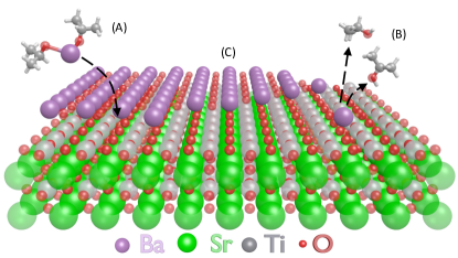
In Solution monolayer epitaxy (SoME) the substrate of choice, in this case a (100) TiO2 terminated SrTiO3, is submersed in a solution of a dissolved precursor of choice, at a temperature slightly lower than its decomposition temperature. Under these conditions the precursor molecules do not decompose in the solution unless they are in close proximity to the surface of the substrate, which catalyzes the decomposition of the precursor and the required material resulting in a monolayer.
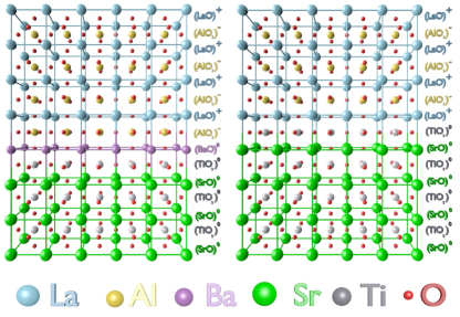
In our case SoME is used to grow a BaO monolayer (termination) on a SrTiO3 substrate as described in Figure 1. We then grow an additional epitaxial layer of LaAlO3 using traditional pulsed laser deposition, giving us a SrTiO3/BaO/LaAlO3 structure as depicted in Figure 2(a) for comparison we show the standard SrTiO3/LaAlO3 interface in Figure 2(b). More details of our process are found in the methods section.
Oxide interfaces can combine degrees of freedom from their constituents with emergent phenomena such as, superconductivity Reyren et al. (2007); Caviglia et al. (2008) magnetism Ben Shalom et al. (2009); Bert et al. (2011); Dikin et al. (2011); Salman et al. (2012); Lee et al. (2013); Ron et al. (2014) tunable spin-orbit interaction Ben Shalom et al. (2010); Caviglia et al. (2010) and quantum transport Tsukazaki et al. (2007); Ron and Dagan (2014); Cheng et al. (2015). The appearance of conductivity in the hallmark interface between LaAlO3 and SrTiO3 has been explained as a result of stacking polar layers of LaAlO3 thus accumulating potential energy Ohtomo and Hwang (2004); Okamoto and Millis (2004); Pentcheva and Pickett (2009); COEY and VENKATESAN (2013); Popović et al. (2008). According to these scenario one expects the two interfaces presented in Figure 2 to have carriers of opposite signs as explained in this figure.
Prior to the LaAlO3 deposition the SoME BaO deposited layer was characterized using an atomic force microscope (AFM) and time of flight secondary ion mass spectroscopy (TOF-SIMS), see Figure 3. Panel (a) shows an AFM topography image of the surface, a smooth surface is observed indicating full coverage of the substrate. Panel (b) shows a spatial distribution map of Ba as measured by TOF-SIMS showing a uniform distribution of Ba on the surface. The combination of these two techniques shows that we have indeed created a smooth single terminated BaO layer on top of the SrTiO3 substrate.
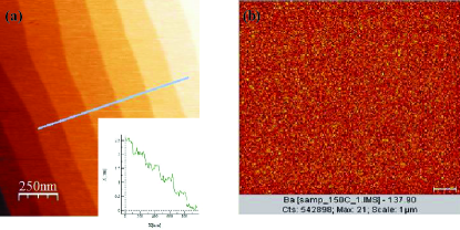
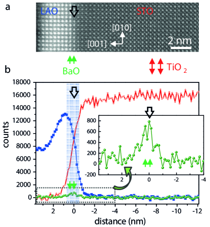
Figure 4(a) shows an atomic-resolution high-angle annular dark-field (HAADF) image of the SrTiO3/BaO/LaAlO3 heterostructure taken from the [100] direction of SrTiO3, whose contrast is roughly proportional to the square of the mean atomic number in the atomic columnsPennycook et al. (2000). By examining the image contrast, the interface between SrTiO3 and BaO/LaAlO3 was identified and marked by the black arrow. The dark contrast on the right side of the interface corresponds to the SrTiO3 substrate since it possesses much smaller numbers with respect to those of BaO and LaAlO3. In the left area, the LaAlO3 and BaO show very bright contrast. However, distinguishing BaO from LaAlO3 in the HAADF image is essentially impossible because the atomic numbers (, ) are almost the same.
Figure 4(b) displays the intensity line profiles of Ti , Ba , and La edges extracted from the background subtracted electron energy-loss spectroscopy (EELS) dataset (supplemental Figure S1(b)), plotted as a function of the distance away from the interface, allowing us to explore the dispersion of elements along the [001] growth direction of LaAlO3/BaO/SrTiO3 heterostructure. Intensity modulations are clearly evident in the Ti and Ba (inset of Figure 4(b)) line profiles, where the modulated peak positions represent the real stacking of the TiO2 and BaO layers, as indicated by the red and green arrows, respectively. This reveals a unique match between the simultaneously recorded HAADF and the EELS stack images, as evidenced in Figure S1. The irradiation damage induced by the electron source, although carefully minimized, inevitably results in a collapse of the near surface structure of LaAlO3 (Figure S1(a)) and leads to the drop of La intensity in Figure 4(b). By checking the intensity modulation of Ba, one can identify the location of the BaO layers which appear to be confined within two atomic layers at the LaAlO3/SrTiO3 interface (inset of Figure 4(b) and Figure S1(b)). In addition, by using the intensity modulation as a reference, the width of the interface can also be estimated as to be three perovskite unit cells, shadowed in light blue of Figure 4(b). Considering the unavoidable broadening effect induced by shape of the electron probe and/or its tailKourkoutis et al. (2010), this value can be regarded as an upper limit of the chemical interdiffusion in the LaAlO3/BaO/SrTiO3 heterostructure.
Wu et al. have shown thin film deposition using dissolved organic precursors Wu et al. (2015). However, in their case TEM imaging indicated films which are far from having epitaxial quality in contrast to our perfect epitaxial monolayer.
In Figure 5(a) we show the sheet resistance of a typical sample measured as a function of temperature. As can be clearly observed is decreasing with temperature, i.e. the interface is metallic. In Figure 5(b) The Hall resistance as function of magnetic field is shown for various gate voltages. The slope of the Hall signal, the Hall coefficient , is negative, corresponding to negative charge carriers. We plot versus gate voltage in Figure 5(c). In a naive, single band, picture the slope of the classical Hall effect is related to the charge carrier density by: . We note that the inferred density increases when applying negative gate voltage. This behavior is in contrast to what is expected from gating an electron doped sample. In Figure 5(d) we show as function of gate voltage. a clear non monotonic behavior is observed.
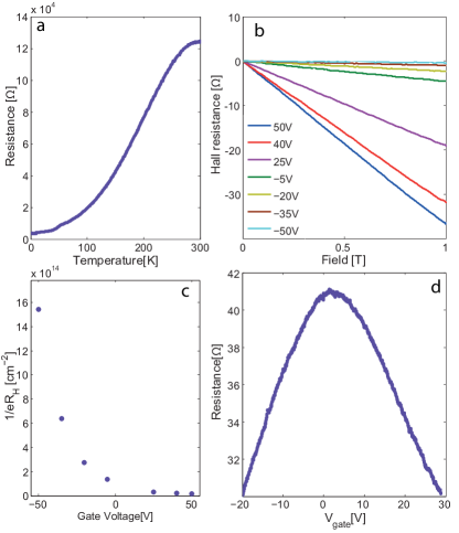
The main evidence for the existence of both holes and electrons at the interface comes from the gate voltage dependence of and . As observed in Figure 5(c) increases by orders of magnitude when applying negative gate voltages, in contrast to the expected behavior of n-type interface. Furthermore is nonmonotonic with gate voltage and has a clear maximum at V.
In the frame of bipolar transport of electrons with density and mobility and holes with density and mobility in the low field limit takes the form: . When the condition is satisfied the Hall signal will be negative as observed in our measurements. Upon applying negative gate voltage decreases and increases. This results in effectively decreasing . Furthermore, behaves nonmonotonically with gate voltage. In SrTiO3/LaAlO3 interfaces decreasing electron density results in lowering of electron mobility, Bell et al. (2009) which result in strong increase of the resistance. Therefore the decreasing resistance observed at VV can be explained only by accumulation of holes.
A close inspection of our data suggests that . For a symmetric electron-hole system the neutrality point should appear at the same gate voltage as the resistance maximum Novoselov et al. (2004). In our system the maximum in resistance appears where the sign of is negative, i.e. . Assuming that the geometrical capacitance for both carriers is the same a decrease in is accompanied by an identical increase in p. Therefore, the decrease in resistance for decreasing gate voltage below V must be in a regime where whereas the regime above must be with . We exclude other scenarios in the supplementary part.
There are many mechanisms that can create n-type doping in SrTiO3 except for the polar scenario including: oxygen vacancies Kalabukhov et al. (2007) and cation mixing Willmott et al. (2007) close to the interface during film growth. However, non of these mechanisms can be responsible for hole doping. We therefore conclude that the polar structure of our samples is responsible for hole doping.
It has been invoked that in n-type LaAlO3/SrTiO3 interface a hole layer is created on the LaAlO3 surface due to charge transfer induced by the polar structure. Such a layer has not been observed and other explanations for the charge transfer have been proposed Yu and Zunger (2014). In order to check if a mobile electron layer is created on the LaAlO3 surface of our nominally p-type hetero-structure we fabricated a device with an additional Au electrode on the LaAlO3 surface. If a mobile electron layer exists it will simply short the top electrode to the contacts. However, we merely observed a negligible leakage current, below our measurement capabilities, between the conducting interface and the top electrode. Finally, we note that while PLD deposited LaAlO3/SrO terminated SrTiO3 interface has been reported to be insulating our LaAlO3/BaO/SrTiO3 interface may be different because of either the preparation method or the variation in chemical composition (Ba instead of Sr).
In summary, we developed a new solution monolayer epitaxy (SoME) method utilizing surface catalysis for depositing crystalline oxide layers. Our new SoME method does not require high temperature environments and it can be used instead of expensive physical deposition techniques or as an addition to them. The great variety of organic precursors make our method versatile and suitable for wide range of materials. To demonstrate our method we grow a BaO layer on top of a TiO2 terminated SrTiO3 . An additional LaAlO3 layer is then deposited using PLD to realize a nominally p-type interface. We interpret the transport measurements of this new interface in the framework of bipolar conductivity where both electrons and mobile holes exist at the interface and can be controlled by gate voltage.
I Appendix: Experimental Methods
I.1 Solution monolayer epitaxy (SoME) of BaO monolayer
In a typical preparation, inside a nitrogen-filled glovebox, about 10 mg of Ba(II) - isopropoxide (Sigma-Aldrich, 99.9%) were weighed and subsequently suspended in 20 mL of anhydrous ethylene glycol (Sigma-Aldrich 99.8%) in a glass vial. The vial was carefully sealed and taken out of the glovebox. It was then sonicated for 5 minutes in order to completely dissolve the barium isopropoxide in the ethylene glycol. The solution was then transferred to a round-bottom flask and a clean TiO2-terminated SrTiO3 substrate was submersed in it. The flask was then purged three times with nitrogen and heated to , (reflux) under constant nitrogen flow. After 30 minutes the flask was let to cool back to room temperature and then opened. The substrate was then washed with acetone and isopropanol to remove the excess solution.
I.2 Pulsed laser deposition and measurements
We grow epitaxial layers of LaAlO3 using reflection high energy electron diffraction monitored PLD on atomically flat BaO terminated SrTiO3 0.5mm thick substrates in standard conditions, oxygen partial pressure of Torr and temperature of , as described in Ben Shalom et al. (2009). Gold gate electrodes are evaporated to cover the back of the substrate. The leakage current is unmeasurably small (1pA). Measurements were performed in a dilution refrigerator with a base temperature of 20mK at magnetic fields of up to 18 Tesla at various gate voltages at Tallahassee National High Magnetic Field Laboratory. Transport results were reproduced for 9, 10, 12 unit cells samples.
I.3 Sample preparation for scanning transmission electron microscopy
orientated cross-sectional lamellae were prepared using a focused ion beam milling FEI Helios NanoLab 400S dual-beam system. The lamellae were thinned by Ar ion milling at 2.5 kV in a Bal-Tec RES-101 system, followed by a 500 eV Ar ion milling to remove the damaged surface layers introduced by previous procedure with a Fischione NanoMill 1040 system.
I.4 scanning transmission electron microscopy
The atomic-resolution HAADF and EELS investigations were performed on an FEI Titan 80-300 microscope equipped with a spherical aberration corrector for the electron probe, running at 300 kV. In STEM mode, a probe size of about 0.1 nm and a semi-convergence angle of 25 mrad were utilized. For HAADF imaging, the inner collecting angle is 70 mrad. For EELS signal collection, the camera length parameter was set to a value of 48 mm, together with a 6.0 mm entrance aperture resulting in a semi-collection angle of about 40 mrad.
II Acknowledgements
Special thanks to J-H Park, D. Graf for help in the magnet lab and to A. Gladkikh for the TOF-SIMS measurements. A.R and A.H equally contributed to this work. This work was supported in part by the Israeli Science Foundation under grant no.569/13 by the Ministry of Science and Technology under contract 3-11875 and by the US-Israel bi-national science foundation (BSF) under contract 2014047. A portion of this work was performed at the National High Magnetic Field Laboratory, which is supported by National Science Foundation Cooperative Agreement No. DMR-0654118, the State of Florida, and the U.S. Department of Energy. Doris Meertens of Research Centre Jülich is thanked for specimen preparation by focused ion beam milling. H. C. Du is thanked for helpful discussions.
References
- Smith and Turner (1965) H. M. Smith and A. Turner, Applied Optics 4, 147 (1965).
- Ma et al. (2008) C. Ma, K.-C. Kim, G. McFarlane, and A. Athalye, in Advanced Semiconductor Manufacturing Conference, 2008. ASMC 2008. IEEE/SEMI (IEEE, 2008), pp. 82–84.
- Reyren et al. (2007) N. Reyren, S. Thiel, A. Caviglia, L. F. Kourkoutis, G. Hammerl, C. Richter, C. Schneider, T. Kopp, A.-S. Rüetschi, D. Jaccard, et al., Science 317, 1196 (2007).
- Caviglia et al. (2008) A. Caviglia, S. Gariglio, N. Reyren, D. Jaccard, T. Schneider, M. Gabay, S. Thiel, G. Hammerl, J. Mannhart, and J.-M. Triscone, Nature 456, 624 (2008).
- Ben Shalom et al. (2009) M. Ben Shalom, C. Tai, Y. Lereah, M. Sachs, E. Levy, D. Rakhmilevitch, A. Palevski, and Y. Dagan, Physical Review B 80, 140403 (2009).
- Bert et al. (2011) J. A. Bert, B. Kalisky, C. Bell, M. Kim, Y. Hikita, H. Y. Hwang, and K. A. Moler, Nature physics 7, 767 (2011).
- Dikin et al. (2011) D. Dikin, M. Mehta, C. Bark, C. Folkman, C. Eom, and V. Chandrasekhar, Physical Review Letters 107, 056802 (2011).
- Salman et al. (2012) Z. Salman, O. Ofer, M. Radovic, H. Hao, M. B. Shalom, K. Chow, Y. Dagan, M. Hossain, C. Levy, W. MacFarlane, et al., Physical review letters 109, 257207 (2012).
- Lee et al. (2013) J.-S. Lee, Y. Xie, H. Sato, C. Bell, Y. Hikita, H. Hwang, and C.-C. Kao, Nature materials 12, 703 (2013).
- Ron et al. (2014) A. Ron, E. Maniv, D. Graf, J.-H. Park, and Y. Dagan, Physical review letters 113, 216801 (2014).
- Ben Shalom et al. (2010) M. Ben Shalom, M. Sachs, D. Rakhmilevitch, A. Palevski, and Y. Dagan, Physical review letters 104, 126802 (2010).
- Caviglia et al. (2010) A. Caviglia, M. Gabay, S. Gariglio, N. Reyren, C. Cancellieri, and J.-M. Triscone, Physical review letters 104, 126803 (2010).
- Tsukazaki et al. (2007) A. Tsukazaki, A. Ohtomo, T. Kita, Y. Ohno, H. Ohno, and M. Kawasaki, Science 315, 1388 (2007).
- Ron and Dagan (2014) A. Ron and Y. Dagan, Physical review letters 112, 136801 (2014).
- Cheng et al. (2015) G. Cheng, M. Tomczyk, S. Lu, J. P. Veazey, M. Huang, P. Irvin, S. Ryu, H. Lee, C.-B. Eom, C. S. Hellberg, et al., Nature 521, 196 (2015).
- Ohtomo and Hwang (2004) A. Ohtomo and H. Hwang, Nature 427, 423 (2004).
- Okamoto and Millis (2004) S. Okamoto and A. J. Millis, Nature 428, 630 (2004).
- Pentcheva and Pickett (2009) R. Pentcheva and W. E. Pickett, Physical review letters 102, 107602 (2009).
- COEY and VENKATESAN (2013) J. COEY and M. VENKATESAN (2013).
- Popović et al. (2008) Z. S. Popović, S. Satpathy, and R. M. Martin, Physical review letters 101, 256801 (2008).
- Pennycook et al. (2000) S. Pennycook, B. Rafferty, and P. Nellist, Microscopy and Microanalysis 6, 343 (2000).
- Kourkoutis et al. (2010) L. F. Kourkoutis, H. Xin, T. Higuchi, Y. Hotta, J. Lee, Y. Hikita, D. Schlom, H. Hwang, and D. Muller, Philosophical Magazine 90, 4731 (2010).
- Wu et al. (2015) Y. Wu, D. Do¨hler, M. Barr, E. Oks, M. Wolf, L. Santinacci, and J. Bachmann, Nano letters 15, 6379 (2015).
- Bell et al. (2009) C. Bell, S. Harashima, Y. Kozuka, M. Kim, B. Kim, Y. Hikita, and H. Hwang, Physical review letters 103, 226802 (2009).
- Novoselov et al. (2004) K. S. Novoselov, A. K. Geim, S. Morozov, D. Jiang, Y. Zhang, S. Dubonos, , I. Grigorieva, and A. Firsov, science 306, 666 (2004).
- Kalabukhov et al. (2007) A. Kalabukhov, R. Gunnarsson, J. Börjesson, E. Olsson, T. Claeson, and D. Winkler, Physical Review B 75, 121404 (2007).
- Willmott et al. (2007) P. Willmott, S. Pauli, R. Herger, C. Schlepütz, D. Martoccia, B. Patterson, B. Delley, R. Clarke, D. Kumah, C. Cionca, et al., Physical review letters 99, 155502 (2007).
- Yu and Zunger (2014) L. Yu and A. Zunger, Nature communications 5 (2014).