The tunneling potential for field emission from nanotips
Abstract
In the quasi-planar approximation of field emission, the potential energy due to an external electrostatic field is expressed as where is the perpendicular distance from the emission site and is the local field enhancement factor on the surface of the emitter. We show that for curved emitter tips, the current density can be accurately computed if terms involving and are incorporated in the potential where is the second (smaller) principle radius of curvature. The result is established analytically for the hemiellipsoid and hyperboloid emitters and it is found that for sharply curved emitters, the expansion coefficients are equal and coincide with that of a sphere. The expansion seems to be applicable to generic emitters as demonstrated numerically for an emitter with a conical base and quadratic tip. The correction terms in the potential are adequate for nm for local field strengths of V/nm or higher. The result can also be used for nano-tipped emitter arrays or even a randomly placed bunch of sharp emitters.
I Introduction
Electron beams find applications in a variety of devices that include the microwave as well as sub-millimeter wave generators and amplifiers, accelerators, microscopes as well for use in lithography, welding, furnace, medical and space applications booske2008 ; whaley2009 ; booske2011 ; whaley2014 ; polk2008 ; graves2012 . Common mechanisms for producing an electron beam are thermionic, field and photo emission. A topic of current research centres around large area arrays of pointed field emitters spindt76 ; spindt91 ; forbes2012 ; zhang2014 ; harris2015 ; jap2016 that offer high brightness, high current density beams having a small spread in energy at low operational temperatures.
Field emission of electrons is commonly studied using a Fowler-Nordheim (FN) type model that involves a planar metallic surface subjected to a uniform external electrostatic field and the attendant image force between the electron and its image due to the grounded metallic plane FN ; Nordheim ; murphy ; jensen2003 ; forbes_deane . Since electron emission is predicted to be weak in the planar case, the focus has been on sharp protrusions from such a surface, where field enhancement is known to occur and can lead to a significant jump in electron emission. An improper surface finish can for example lead to undesirable dark currents in accelerators while properly grown nanotube arrays on a planar substrate can be the basis of a high performance cold cathode. In both cases, the protrusions are sharp and only their tips act as electron emitters. Field emission in such cases is handled by a quasi-planar extension where the local electric field continues to be uniform across the tunneling region but its magnitude is enhanced by the field enhancement factor . However, when the protrusions are sharp and the apex radius of curvature is only a few nanometers, the local electric field decreases significantly even within the tunneling regime. This change in local field away from the surface of curved emitters should thus be incorporated as corrections in order to predict the emitted current density accurately.
The nonlinear nature of the external field near the surface of curved emitters is well known cutler93a ; cutler93b ; fursey ; forbes2013 . For exactly solvable problems such as the hyperboloid, the deviation from the planar result has been demonstrated in the form of nonlinear FN-plots and the current densities were found to differ by orders of magnitude cutler93a ; cutler93b . In general however, a first approximation in dealing with curved emitters is to treat the surface locally as a sphere having the same local radius of curvature. Thus, the external potential may be expressed locally as fursey ; forbes2013
| (1) |
where is the local radius of curvature and is the perpendicular distance from the surface. For axially symmetric emitters, the form of the nonlinear external potential has recently been studied using a different approachKX . It has been shown that along the symmetry axis of the emitter, for , the external potential energy takes the form
| (2) |
where is the apex radius of curvature and the normal distance is measured from the apex.
The validity of the local spherical approximation can be scrutinized using exact results for curved emitters such as the hyperboloid or hemi-ellipsoid. A similar approach for the image potential shows that for the hyperboloid, where exact results for the image charge potential due to a ring of charges is known jensen_image , the spherical approximation is found to hold BR2017a near the tip of sharp hyperboloids when the local radius of curvature considerably exceeds the tunneling distance.
The approach that we adopt here makes use of the exact results for the hemi-ellipsoid and hyperboloid emitters to derive a correction to Eq. 2 and determine the conditions under which it is identical for the two emitters. We then show that an identical result exists for the sphere provided corrections to Eq. 1 are incorporated. Our derivation also brings out the role of the principle radii of curvature () and the added clarification that the spherical approximation, where applicable, must be used with except at the apex where . Finally, the applicability of the result is tested numerically for a conical emitter with a quadratic tip and found to be in good agreement.
II Potential variation normal to the surface
We shall first deal with the potential variation along field lines close to the surface of a hemiellipsoid and a hyperboloid kos ; pogorelov . In both cases, the structure is assumed to be vertically aligned () in the presence of an external field. It is convenient to work in prolate spheroidal coordinate system (). These are related to the Cartesian coordinates by the following relations:
| (3) |
Note that a surface obtained by fixing in this coordinate system is an ellipsoid while defines a hyperboloid.
For a hemiellipsoid in an external field , the field lines close to the surface are curves. For a hyperboloid diode with both the cathode and anode as hyperboloid surfaces, the field lines are always curves. Further, since we are concerned with potential variation over a distance of around nm at moderate fields of V/nm, we shall assume that the curved field lines are approximately straight over this distance. Its validity is tested in the appendix for a hemiellipsoid where it is shown using a Taylor expansion, that close to the apex from where field emission predominantly occurs, the straightness assumption is largely valid.
II.1 hemiellipsoid
Consider a hemiellipsoidal emitter, , on a grounded conducting plane, placed in an external electrostatic field . The solution of Laplace equation may be written askos ; pogorelov ; jap2016
| (4) |
where , is the height and is the apex radius of curvature. The point may lie on the hemiellipsoid surface or outside. We wish to determine the variation in potential close to the surface along the field line at the point .
Using Eq. 4, the electrostatic potential at this local point outside the surface can be calculated as
where
| (5) | |||||
| (6) |
Using the expansion the above expression for the potential can be approximated as
which on simplifying and keeping terms upto , takes the form
Rewriting in terms of magnitude of the local field
| (7) |
and the normal distance from the point
| (8) |
where
| (9) |
the potential can be expressed as
| (10) | ||||
For an ellipsoid , the principal local radii of curvature at the point () are
| (11) | |||||
| (12) |
while the Gaussian radius of curvature is
| (13) |
Thus, Eq. 10 can be further simplified as
| (14) |
and forms the central result of this paper. It can be used to estimate the tunneling transmission coefficient and hence the current density at a point close to the emitter apex.
Note that Eq. 14 represents approximately the potential variation along the normal to a point on the surface of the hemiellipsoid. However, in the apex neighbourhood of a sharp emitter, Eq. 14 does represent the normal potential variation close to the surface quite accurately (see appendix) and can thus be used to determine emission currents.
II.2 Hyperboloid
The hyperboloid emitter surface is defined by while a flat anode is placed a distance below the tip. In the transformation equations of Eq. 3, where is the apex radius of curvature hyperbola . The derivation of the potential variation follows a similar line. If the potential difference between the anode and cathode is , the potential at any point can be expressed as
| (15) |
Thus for small excursions along the field line starting from the point () on the hyperboloid surface, the potential
| (16) | ||||
Keeping terms upto , we have
| (17) | ||||
In terms of the normal distance
| (18) |
and the local electric field
| (19) |
the potential variation can be expressed as a function of as
| (20) |
where is a principal radius of curvature for the hyperboloid evaluated at the point (). The respective radii of curvature can be expressed as
| (21) | |||||
| (22) | |||||
| (23) |
For a reasonably sharp emitter tip, is close to unity. As an illustration, for nm and nm, while for nm and nm, . Thus, setting to be 1,
| (24) |
as in the case of hemiellipsoid. As before, Eq. 24 is more accurately the potential variation along field lines of constant and only approximately so along the normal distance. Close to the tip of a sharp hyperboloid however, it is expected that Eq. 24 is a good approximation for the potential variation normal to the emitter near the apex.
II.3 The Sphere
For a grounded conducting sphere of radius in an electric field , the potential outside the sphere is
| (25) |
Writing ,
| (26) |
Writing and neglecting the second term leads us to Eq. 1. However, since we are interested in a correction term of the order of , the second term must be retained. Now assuming ,
| (27) | |||||
| (28) |
which is identical to the result obtained above for the hemi-ellipsoid and the hyperboloid.
II.4 Generic emitter tips
A derivation of a corrected formula for the external potential variation applicable to generic emitter is not readily available. However, we shall investigate the applicability of Eq. 24 for generic emitters with parabolic tips. Note that cylindrically symmetric emitter tips that are vertically aligned can be approximated as
| (29) | |||||
| (30) |
where is the magnitude of the apex radius of curvature, , is the height of the emitter and we have assumed that the tip is not flat (). Also, since field emission occurs close to the tip, higher order terms in can be ignored in the expansion of .
Eq. 30 can be used to find the local and gaussian curvatures in terms of the apex radius of curvature. Moreover, recent results B2017b show that local surface electric field around the tip can be expressed in terms of the local electric field at the apex () and a generalized factor:
| (31) |
where is the field enhancement factor at the apex and is the height on the emitter surface measured from the conducting plane.
For a surface parameterized as (), where and , the local Principal and Gaussian radii of curvature are respectively
| (32) | |||||
| (33) | |||||
| (34) |
Thus, for quadratic emitters, and in Eq. 24 are given by Eq. 31 and 33 respectively if the apex radius of curvature and field enhancement factors are known. Alternately, they can be computed at each point on the emitter surface if the exact numerical solution for the potential is available. As in case of the hyperboloid, Eq. 24 is expected to hold for general quadratic emitters that are sharp.
III Numerical Results
We shall first make a crude estimate of the domain of validity of Eq. 24 for a typical local electric field V/m. For an emitter with work function of eV, the tunneling distance at this local field is about nm. At the apex, with nm, the quadratic term is about of the linear while the cubic is about of the linear. Thus, along the symmetry axis, the neglect of terms higher than cubic appears justified when nm.
Away from the emitter apex, the principle radius of curvature increases (albeit slowly compared to ) for typical quadratic tips. At the same time, the local electric field decreases for a given external electric field. Thus, while the tunneling distance increases marginally, the domain of validity of Eq. 24 also increases. In the following, we shall explore the difference between the exact current density and the one obtained using the approximate potential of Eq. 24, for various emitter shapes and position.
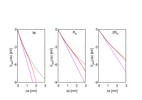
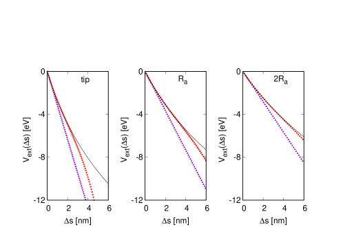
First, we consider a hemiellipsoidal emitter on a grounded conducting plane placed in a uniform electric field. Fig. 1 shows the potential energy due to the external field at three locations on the emitter surface (i) at the tip (ii) at (iii) at . At the tip where nm, the exact potential and Eq. 24 match quite well to about nm while at locations (ii) and (iii) the agreement gets better since increases. Fig. 2 shows a similar plot for nm and V/m. The agreement at all three location now gets better. For an even larger apex radius nm, the agreement extends beyond nm at all three locations.
We next turn our attention to the tunneling current densities generated using these potentials. Assuming a free electron model, the current density is evaluated at zero temperature as
| (35) |
where is the transmission coefficient at energy , is the mass of the electron, is the magnitude of the electron charge and is the Fermi level. Instead of using the WKB expression for the transmission coefficient, we shall determine numerically using suitable boundary conditions for the 1-dimensional Schrödinger equation and a modified transfer matrix method DBVishal . In the results presented here, curvature corrections to the image potential have been neglected in order to bring out the role of corrections to the external potential.
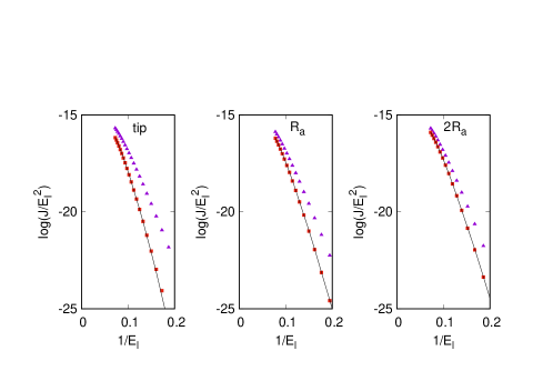
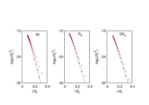
The corresponding current densities for nm are shown in Fig. 3 at the locations mentioned earlier. Clearly the two correction terms in the potential (see Eq. 24) are adequate to reproduce the exact results. For m ( nm), the current density is shown in Fig. 4. The agreement with the exact result remains excellent using Eq. 24 while the agreement between the exact and quasi-planar case improves considerably as expected.
We next turn our attention to a case where the analytical solution for the potential is not known. Using a suitable nonlinear line-charge of height placed on a grounded conducting plane in the presence of a uniform electric field, a conical zero-potential surface is obtained of height m, base radius m, having a rounded top with an apex radius of curvature nm. The emitter tip is modeled very wellB2017b by the quadratic .
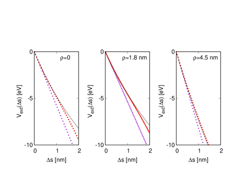
Fig. 5 is a plot of the potential energy variation along the normal to the emitter surface. The points (from left to right) are located at (i) (the emitter tip) (ii) nm and (iii) nm. The exact potential is calculated using the line charge distribution. Clearly, Eq. 24 provides a fair approximation to the exact potential in the tunneling regime. It gets marginally better away from the apex due to the increase in but thereafter minor deviations in the tunneling region occur, perhaps due to the uncertainty in the 4/3 multiplying factor.
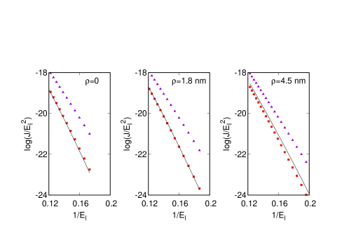
The corresponding current densities are shown as a Fowler-Nordheim plot in Fig 6. In the first two cases, the current densities using Eq. 24 for the external potential are in good agreement with the exact result (solid line) obtained using the nonlinear line charge distribution. In the third case (plot to the right), Eq. 24 underestimates the current density marginally. The difference with the quasi-planar case is again substantial especially at smaller values of local field , in all three cases.
In order to determine the effectiveness of Eq. 24 in determining the total electron current from a single emitter, we have computed the emitter current at two values of the external field, . At V/m (corresponding to a local apex field V/m), the currents obtained from the quasi-planar approximation, Eq. 24 and the exact potential are A, A and A respectively. While the last two values are close, the quasi-planar current is nearly 7 times more. At the higher external field V/m, the currents obtained from the quasi-planar approximation, Eq. 24 and the exact potential are 0.36 mA, 0.205 mA and 0.220 mA respectively. The last two values are still close while the quasi-planar approximation improves considerably.
IV Discussion and Conclusions
The study of two analytically solvable models, the hemiellipsoid on a conducting plane and the hyperboloid diode, led us to Eq. 24. In both cases, when the emitter is sharp, Eq. 24 is accurate near the apex for short excursions in the normal direction. An identical result was derived for a sphere thereby establishing that the spherical approximation for curved emitters (where applicable) must be used with the the second principle radius of curvature as the radius of the sphere.
Finally, we have also numerically explored the validity of Eq. 24 for an analytically unsolvable case, the cone with a quadratic tip. Our numerical studies show that in all the examples, the current densities obtained using Eq. 24 agree well with the exact result near the emitter tip and show a considerable improvement compared to the quasi-planar case in predicting the emitter current. At low external field strengths, where the difference with the quasi-planar case is almost an order of magnitude, Eq. 24 predicts the current with less than error. At higher field strengths, the quasi-planar result improves but is still poor compared to the prediction of Eq. 24. The results presented here have also been tested for a cylindrical emitter with a quadratic tip.
While the preceding discussion has centred around a single sharp emitter, it is clear that the form of the external potential remains the same even if the emitter is part of a regular array or a randomly distributed bunch of emitters, so long as the emitter tip is smooth and parabolic. For a bunch of emitters with identical height and apex radius of curvature, the only quantity in Eq. 24 that depends on the neighbourhood is the local external electric field, . This is determined by the extent of shielding which must be determined separately before calculating the field emission current.
In conclusion, the quasi-planar approximation to the potential due to the external field leads to large errors in emitted current when the apex radius of curvature nm and the applied external field is small. For , Eq. 24 seems to provide a very good approximation to the external potential and accurately reproduces the emitter current. Finally, in addition to curvature effects in the external potential, corrections to the image potential are also important and must be included in determining the emitter current.
V Acknowledgement
The authors acknowledge several useful discussions with Dr. Raghwendra Kumar.
VI Appendix
For orthogonal co-ordinate systems in which the Laplace and Schrödinger equations are separable, tunneling transmission coefficients along field lines can be calculated using the standard 1-d formalisms. In the general case however, curved field lines would necessitate use of the multi-dimensional tunneling formalism. In view of a possible general applicability of Eq. 14 to non-separable systems, we have instead chosen to express the external potential in terms of the normal distance so that standard 1-dimensional tunneling results can be used. This also leaves open the possibility of incorporating the results of this paper in a modified Fowler-Nordheim equation.
The assumption so far in using the normal distance has been that field lines are more or less straight over the tunneling distance of about nm at moderate local field strengths. In the following, we shall test this assumption for a hemiellipsoid by Taylor expanding the potential along the normal direction and comparing with Eq. 14.
Consider a point () on the hemiellipsoid . A point outside, at a distance normal to the hemiellipsoid at () can be written as
| (36) |
where , and . The point () can be assumed to lie on another hemiellipsoid and is defined alternately by the co-ordinates () = () where and can be computed by demanding that the point outside satisfies the ellipsoid/hyperboloid equation. Thus, is determined using
| (37) |
while can be evaluated either using
| (38) |
or using and Eq. 37. The solutions, to the accuracy required, can be expressed respectively as
| (39) | |||||
| (40) |
where
| (41) | |||||
| (42) | |||||
| (43) |
while
| (44) | |||||
| (45) |
with
| (46) | |||||
| (47) |
A Taylor expansion of the potential at the point () along the normal can be expressed as
| (48) | |||
where and and are given by Eqns. (39) and (40) respectively. Clearly, this expansion suffices to expand the potential upto since is zero. Also, since the term contributes , it will be ignored henceforth. The relevant partial derivatives can be evaluated as follows:
| (49) | |||||
| (50) | |||||
| (51) | |||||
| (52) | |||||
| (53) |
Collecting together terms , the potential for the hemiellipsoid is expressed as
| (54) |
where
| (55) | |||||
| (56) | |||||
| (57) |
Consider now a sharp hemiellipsoid emitter for which and a point () on its surface at a height . At the apex, , while the apex neighbourhood from where emission predominantly takes place corresponds generally to . The following approximations can then be made:
| (58) | |||||
| (59) | |||||
| (60) | |||||
| (61) | |||||
| (62) | |||||
| (63) |
A comparison of the terms in at yields
| (64) | |||||
| (65) |
while the terms in at are
| (66) | |||||
| (67) | |||||
| (68) | |||||
| (69) |
Thus, for a sharp emitter with , in the region close to the apex () from where electron emission predominantly occurs at moderate fields, while . This leads to Eq. 14.
In part therefore, the results obtained using Eq. 14 are in good agreement because the apex neighbourhood contributes substantially to the current. Our results show that at a local fields of V/nm, the region contributes as much as 70% to the total current. There is also a cancellation of effects. The correction to the coefficient of the term leads to an increase in current while the correction to the coefficent of the term leads to a decrease. Our studies for various field strengths and apex radius of curvature, show that Eq. 14 provides an optimum description of the external potential.
VII References
References
- (1) J. H. Booske, Phys. Plasmas 15, 055502 (2008).
- (2) D. R. Whaley, R. Duggal, C. M. Armstrong, C. L. Bellew, C. E. Holland, and C. A. Spindt, IEEE Trans. Electron Devices 56, 896 (2009).
- (3) J. H. Booske, R. J. Dobbs, C. D. Joye, C. L. Kory, G. R. Neil, G.-S. Park, J. Park, and R. J. Temkin, IEEE Transactions on Terahertz Science and Technology, 1, 54 (2011).
- (4) D.R. Whaley, IEEE Trans. Electron Devices 61, 1726 (2014).
- (5) J. E. Polk, M. J. Sekerak, J. K. Ziemer, J. Schein, N. Qi, and A. Anders, IEEE Trans. Plasma Sci. 36, 2167 (2008).
- (6) W. S. Graves, F. X. Kärtner , D. E. Moncton , and P. Piot, Phys. Rev. Lett. 108, 263904 (2012).
- (7) C. A. Spindt, I. Brodie, L. Humphrey, and E. R. Westerberg, J. Appl. Phys. 47, 5248 (1976).
- (8) C. A. Spindt, C. E. Holland, A. Rosengreen and I. Brodie, IEEE Trans. on Electron Devices, 38, 2355 (1991).
- (9) R. G. Forbes, Nanotechnology 23, 095706 (2012).
- (10) Z. Zhang, G. Meng, Q. Wu, Z. Hu, J. Chen, Q. Xu and F. Zhou, Scientific Reports 4, 4676 (2014).
- (11) J. R. Harris , K. L. Jensen , D. A. Shiffler , and J. J. Petillo , Appl. Phys. Lett. 106, 201603 (2015).
- (12) D. Biswas, G. Singh and R. Kumar, J. App. Phys. 120, 124307 (2016).
- (13) R. H. Fowler and L. Nordheim, Proc. R. Soc. A 119, 173 (1928).
- (14) L. Nordheim, Proc. R. Soc. A 121, 626 (1928);
- (15) E. L. Murphy and R. H. Good, Phys. Rev. 102, 1464 (1956).
- (16) K. L. Jensen J. Vac. Sci. Technol. B, 21, 1528 (2003).
- (17) R. G. Forbes and J. H. B. Deane, Proc. Roy. Soc. A 463, 2907 (2007).
- (18) P. H. Cutler, J. He, N. M. Miskovsky, T. E. Sullivan and B. Weiss, J. Vac. Sci. Technol. B 11, 387 (1993).
- (19) P. H. Cutler, J. He, J. Miller, N. M. Miskovsky, B. Weiss and T. E. Sullivan, Prog. Surf. Sci. 42, 169 (1993).
- (20) G. N. Fursey and D. V. Glazanov, J. Vac. Sci. Technol. B 16, 910 (1998).
- (21) A. Fischer, M. S. Mousa and R. G. Forbes, J. Vac. Sci. Technol. B 31, 032201 (2013).
- (22) A. Kyritsakis and J. P. Xanthakis, Proc. R. Soc. London, A471, 20140811 (2015).
- (23) K. L. Jensen, D. A. Shiffler, J. R. Harris, I. M. Rittersdorf and J. J. Pettilo, J. Vac. Sci. Technol. B35, 02C101 (2017).
- (24) D. Biswas and Rajasree R., Phys. Plasmas 24, 073107 (2017); ibid. 24, 079901 (2017)
- (25) H. G. Kosmahl, IEEE Trans. Electron Devices 38, 1534,1991.
- (26) E. G. Pogorelov, A. I. Zhbanov and Y.-C. Chang, Ultramicroscopy 109, 373 (2009).
- (27) Changing the tip-anode distance, , changes the hyperboloid .
- (28) D. Biswas, G.Singh, S.G.Sarkar and R.Kumar, “Variation of field enhancement factor near the emitter tip”, https://arxiv.org/abs/1705.06867
- (29) D. Biswas and V. Kumar, Phys. Rev. E 90, 013301 (2014).