Two-dimensional electron gas at the interface of
the ferroelectric-antiferromagnetic heterostructure
Ba0.8Sr0.2TiO3/LaMnO3
Abstract
The temperature dependence of the electrical resistivity of the heterostructures consisting of single crystalline LaMnO3 samples with different crystallographic orientations covered by the epitaxial ferroelectric Ba0.8Sr0.2TiO3 film has been studied. Results obtained for the heterostructure have been compared with the electrical resistivity of the single crystalline LaMnO3 without the film. It was found that for the samples with the films where the polarization axis is perpendicular to the crystal surface the electrical resistivity strongly decreases, and at the temperature below 160 K undergoes the insulator-metal transition. calculations were also performed for the structural and electronic properties of the BaTiO3/LaMnO3 heterostructure. Transition to the 2D electron gas at the interface is shown.
pacs:
64.10.+h, 77.22.Jp., 77.84.-sThe high-mobility electron gas has been observed the first time in 2004 S1 at the interface between LaAlO3 (LAO) and SrTiO3 (STO). Later on similar heterostructures consisting of a nonmagnetic and insulating oxides have been extensively studied. In particular, it was found that nanometer-thick metallic phase (two-dimensional electron gas - 2DEG) is formed in the STO layers at the LAO/STO interface when the number of LAO overlayers exceeds three S2 . Below 300 mK S3 the system passes into the superconducting state. The density of the current carriers in such heterostructure reaches the value of 31013 cm-2. In addition, the ferromagnetic order has also been found in the system S4 . 2DEG have been later found in other non-magnetic dielectrics, e.g., in KTaO3/SrTiO3 S5 and CaZrO3/SrTiO3 S6 . Also, 2DEG has been found at the interface between Mott-insulators and a magnetic layer, in particular, with ferromagnetic GdTiO3 S7 , and also at the interface with antiferromagnetic SmTiO3 S8 , LaTiO3 S9 , with maximum possible electron density of 31014 cm-2. Later on S11 , formation of 2DEG has been demonstrated in NdAlO3/SrTiO3, PrAlO3/SrTiO3, NdGaO3/SrTiO3, and also in LaGaO3/SrTiO3 S10 heterostructure.
It is supposed that the appearance of conductivity is coupled with the structural and, consequently, electronic reconstructions. However, so far there is no unambiguous explanation and the theory which can be able to explain all phenomena found in those systems. One of the most important feature related to the 2DEG formation is the local polarity of the (LaO)+1 and (AlO layers inside the LAO slab. In this paper in order to investigate the correlations between structural distortions, electronic reconstruction and polarity, we have chosen the BaTiO3/LaMnO3 (BTO/LMO) heterostructure, where all layers BaO and TiO2 in simple electronic limit are ”electrically neutral”, but there is a ferroelectric polarization due to the Ti+4 atoms displacements out of octahedron center in the BTO. The direction of such a polarization can be switched by an external electric field, what is impossible to be done in the LAO slab, because an external influence cannot change the sequence of (LaO)1+ and AlO layers. Moreover it is very important that in our case there is no need to make a very high-quality ferroelectric-antiferromagnetic boundary, because the polarization arises in the volume of the ferroelectric (This differs from the case of LAO where, for the appearance of polarization on the interface, it is necessary to obey strictly the sequence of (LaO)+1 and (AlO layers). Besides, the BTO/LMO system is attract the interest because it contains antiferromagnetic LaMnO3, which can be transferred to ferromagnetic state by increasing the concentration of the free carriers deGennes ; Dog (the reason for that is an increasing the indirect ferromagnetic exchange). That can be realized by doping of the LMO deGennes ; Dog . It can be further expected that increasing the free charge carriers can lead to the local ferromagnetic order and magnetoresistivity Dog in a system with 2DEG. Therefore, there is an opportunity to switch both conductivity by an electric field (trigger effect), and the magnetic order (magnetoelectric effect) in the heterostructures similar to BTO/LMO. We present the results on of calculation of the structural and electronic properties calculations for the BaTiO3/LaMnO3 (BTO/LMO) heterostructure, as well as experimental study of the resistivity of the Ba0.8Sr0.2TiO3/LaMnO3 (BSTO/LMO) heterostructure with 350 nm thickn BSTO layer.
For the experimental study we used the single crystalline LMO. On their modified surface the epitaxial films of the BSTO were deposited using the sputtering technique. Our sample choice is based on the following facts: (1) preparation technique for the single components was previously well developed and tested S23 ; S21 ; S22 ; (2) properties of a0.8S0.2TO3 and BTO are not much different; (3) transition temperature to the ferroelectric state is relativity high S21 : 540 K for 300 nm-thick films S21 . Properties of 2DEG slightly change starting from the certain thickness of the part of the system which demonstrates polar properties indicated by our modeling. That is why we used 350 nm-thick films. In the present investigations it was important to find conducting state and to fix it reliably whereas the influence of the thickness of the ferroelectric component on the properties of 2DEG is the aim of our further investigations. The thin film of Ba0.8Sr0.2TiO3 (BSTO) was sputtered on the top of the single crystalline LaMnO3 samples. The resistivity measurements were performed by a four-point probe method. In parallel we started the first-principles calculations in order to determine structural and electronic properties of the BTO/LMO heterostructure.
First of all, we present the results of our calculations of the properties of the BTO/LMO heterostructure. We used density functional theory (DFT) as a main method S14 . Exchange and correlational effects were accounted by generalized gradient approximation (GGA) S17 . Kohn-Sham equations were solved using the plane-wave basis set (PAW) S18 , realized within the VASP code S15 , implemented into the MedeA software S19 . The cut-off energy were chosen to be 400 eV, The force tolerance was 0.05 eV/Å and the energy tolerance for the self-consistency loop was eV. The Brillouin zones were sampled including -points. Since there is a strong correlation between -electrons in our system the GGA+ correction were added to our computational scheme S16 . The parameter were added to La 4, Ti 3 Mn 4 (=8 eV, 2 eV 4 eV, respectively). All calculations were performed taking into account magnetic nature of the material.
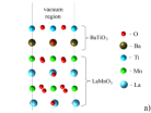
In Fig. 1a half of the unit cell of the studied system LMO/BTO with BaO interface layer is presented whereas the second part is a mirror copy with respect to the central LaO layer. Cell parameters for the bulk LMO with orthorhombic structure obtained after optimization equal to =5.650 Å, =5.616 Å, =7.935 Å (experimental values: =5.537 Å, =5.749 Å, =7.665 Å). For modeling the heterostructure the LMO central slab was enlarged by 1.5 times and bounded by a varing number of BaTiO3 layers with interface BaO or TiO2 layers on both sides. Such a unit cell guarantee the absence of the dipole moment and additional polarity which might arise due to non-symmetric structure. In order to avoid interaction of the surfaces and slabs with their periodic images, a 20 Å vacuum region was added. In plane cell parameters were fixed, whereas atom positions were allowed to relax during the optimization procedure.
After the optimization of both interface types (first corresponds to BaO interface layer, second – to the TiO2 layer) it was found that in the first case, the total energy of the system is lower, what means that the structure is more stable. That is why all further reasoning will be presented to the most stable configuration. It is seen from Fig. 1a that in the near-surface TiO2 layer the Ti atoms move out of the oxygen planes by 0.15 Å. That leads to a dipole moment induction towards the interface. Calculations involving higher number of the BTO layers are required to get a full picture of structural distortions, what will be done in our further publications.
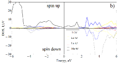
In order to determine the electronic properties of the studied structure the density of states (DOS) spectrum has been calculated taking into account magnetic features of LMO. Fig. 1b shows the atom-resolved DOS for Mn, La and Ti. It is seen that already with one BTO layer the band gap is closed. Mn atoms orbitals cross the Fermi-level. Besides, the total magnetic moment induction takes place which is mainly corresponds to Mn atoms forms.
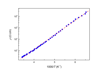
Measurements were performed for three types of samples: (1) sample N1 is a heterostructure based on the single crystalline LMO with a BSTO film on the top of it ( axis of the LMO is parallel to the deposition plane); (2) sample N2 is a heterostructure based on the single crystalline LMO with a BSTO film on top of it ( axis is perpendicular to the deposition plane); (3) samples N01 and N02 are the single crystalline LMO without films with polarization axis as in the cases of N1 and N2, respectively. X-ray measurements has shown that: 1) for the N1 sample the c axis (along which the spontaneous polarization is detected) is parallel to the film plane; (2) for the N2 samples c axis is perpendicular to the film plane. The reason for that is the lattice mismatch: in the first case the LMO substrate is stretchy with respect to the film, whereas in the second case – compressive S22 . In both cases this is determined by the difference in unit cell parameters of the single crystal and film. The electrical resistivity measurements were performed using the standard four-point method for N01 and N02 samples (the current is perpendicular to the axis of the LMO single crystal). The results for N2 sample are presented in Fig. 2. The electrical resistivity shows an activation behavior which is typical for the semiconducting type of conductivity and corresponds to the behavior of the electrical resistivity of the LMO, measured for the similar samples Dog ; S23 . For modeling the behavior of the specific electrical resistivity we used the formula: exp (is shown in Fig. 2 by red dashed line for the surface orientation perpendicular to the axis). Using it we got the following values of constants: 10-3 cm, .
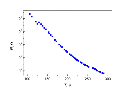
Electrical resistivity has been measured for N1 sample by a four-point probe method as well. In this case the axis of the LMO single crystal is perpendicular to the current. Results are presented in Fig. 3. In this case the resistivity of the N1 sample shows the activation behavior at the whole experimental temperature range. Results for N2 sample are shown in Fig. 4. Since the axis of the LMO single crystal is perpendicular to the film plane, the current is perpendicular to the axis. At high temperatures the electrical resistivity of the N2 sample demonstrates activation behavior, whereas at the temperature below 160 K it has metallic-like features. At the same time, the total electrical resistivity of the N2 sample is few times less than at the whole experimental temperature range ( is resistivity of the sample without film, it was obtained by data from Fig. 2 and plotted in Fig. 4). A sharp drop of the resistivity at low temperature may be an evidence for 2DEG formation.
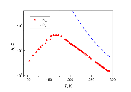
Let us analyze the obtained results and perform some estimations of the parameters of the emerging state. Suppose that the electrical current at the whole measuring range flows over three layers with different transport properties: (1) the first is the LMO single crystal with the resistivity (is shown by dashed line in Fig. 4); (2) the second is the ferroelectric layer with a very high resistivity (the current is almost zero) and (3) the last one is a layer with a high charge carriers density inside the LMO slab near the interface with a thickness and resistivity . Then, can be calculated by formula ), where is a measured resistivity of the sample. Near the temperature of the liquid nitrogen . Taking into account that:
| (1) |
Here is the specific resistivity of the LMO in the metallic state, is the length of the area where conductivity has been measured (distance between the potential contacts cm), is a transverse dimension of the measuring area (cm). For a surface concentration of charge carriers , where is a volume charge carriers concentration. Taking into account (1), can be rewritten as:
| (2) |
If we take the number of the charge carriers (the doping level) per unit cell of the order of , which is typical for metallic conductivity of the lanthanum manganite at low temperatures and write the volume charge carriers concentration as ( are lattice parameters for the LMO unit cell), then using known values for a manganite’s resistivity Ohmcm near the liquid nitrogen temperature for compounds with similar charge carriers density S23 , we can obtain the surface charge carriers concentration: cm-2. This gives the following estimation of the layer thickness, where the high mobility electron gas forms: , nm (=7.665 Å is LMO unit cell size in the -axis direction).
In conclusion, it should be noted that the regimes of deposition of the BSTO films gives as a possibility to avoid the doping of substrate by the elements from the film S21 ; S22 . According to this one can be sure that all observations are not due to implantation of some elements (like Sr) into wear-surface of the single crystalline LMO. The fact that high mobility electron gas is observed only for one LMO orientation (sample N2) and is not for another orientation (sample N1) also indirectly confirms the above-mentioned fact. Magnetic properties of the BSTO/LMO heterostructure, effect of magnetic field on transport properties of the 2DEG in this heterostructure, as well as ferroelectric layer thickness effect on 2DEG properties will be presented in next publications.
Hence in our paper we have presented the calculations of the structural and electric properties of the ferroelectric/antiferromagnet (BaTiO3/LaMnO3) heterostructure. The role of the structural reconstruction in formation of metallic state at the interface is revealed. Electrical resistivity has been measured for single crystalline antiferromagnetic LaMnO3 samples. After that the epitaxial ferroelectric Ba0.8Sr0.2TiO3 film was deposited on the LMO sample using the magnetron sputtering technique. The measurements demonstrated that the resistivity of the single crystalline antiferromagnetic LaMnO3 sample with deposited film of Ba0.8Sr0.2TiO3 decreases strongly, and below the temperature of 160 K passes to a metallic-like behaviour. The latter is observed only when the polarisation axis of the ferroelectric film is perpendicular to the single crystal surface and the film plane is perpendicular to the axis of the LaMnO3 single crystal. In this case, the substrate has a compressive effect on the film.
Authors thank Yu. I. Golovko for the assistance in the samples characterisation, and S. . Migachev in the modification of the single crystal surface before the film deposition. This study was supported by the Supercomputing Center of Lomonosov Moscow State University. The authors from Kazan Federal University acknowledge partial support by the Program of Competitive Growth of Kazan Federal University.
References
- (1) A. Ohtomo and H. Y. Hwang, Nature 427, 423 (2004), 5, 204 (2006).
- (2) S. Thiel, G. Hammerl, A. Schmehl, C. W. Schneider, and J. Mannhart, Science 313, 1942 (2006).
- (3) N. Reyren, S. Thiel, A. D. Caviglia, L. Fitting Kourkoutis, G. Hammerl, C. Richter, C. W. Schneider, T. Kopp, A.-S. Rüetschi, D. Jaccard,M. Gabay, D. A. Muller, J.-M. Triscone, and J. Mannhart, Science 317, 1196 (2007).
- (4) A. Brinkman, M. Huijben, M. Van Zalk, J. Huijben, U. Zeitler, J. C. Maan, W. G. van der Wiel, G. Rijnders, D. H. A. Blank, and H. Hilgenkamp, Nature Mater. 6, 493 (2007).
- (5) A. Kalabukhov, R. Gunnarsson, J. Börjesson, E. Olsson, T. Claeson, and D. Winkler, Phys. Rev. B 75, 121404 (2007).
- (6) W. Chen, L. Li, J. Qi, Y. Wang, and Z. Gui, J. Am. Ceram. Soc. 81, 2751 (1998).
- (7) P. Moetakef, T. A. Cain, D. G Ouellette, J. Y Zhang, D. O. Klenov, A. Janotti, Ch. G. Van de Walle, S. Rajan, S. J. Allen, and S. Stemmer, Appl. Phys. Lett. 99, 232116 (2011).
- (8) C. A. Jackson and S. Stemmer, Phys. Rev. B 88, 180403 (2013).
- (9) J. Biscaras, N. Bergeal, A. Kushwaha, T. Wolf, A. Rastogi, R. C. Budhani, and J. Lesueur, Nature Communications 1, 89 (2010).
- (10) A. Annadi, A. Putra, Z. Q. Liu, X. Wang, K. Gopinadhan, Z. Huang, S. Dhar, T. Venkatesan, and Ariando, Phys.Rev.B. 86, 085450 (2012).
- (11) P. Perna, D. Maccariello, M. Radovic, U. Scotti di Uccio, I. Pallecchi, M. Codda, D. Marré, C. Cantoni, M. Varela, S. J. Pennycook, and F. M. Granozio, Appl. Phys. Let. 97, 152111 (2010).
- (12) P.-G. de Gennes, Physical Review 118, 141 (1960).
- (13) Elbio Dagotto, Takashi Hotta, Adriana Moreo, Physics Reports 344, Issues 1-3, 1-153 (2001).
- (14) A. A. Mukhi, V/ Yu/. Ivanov, V. D. Travkin, S. P. Lebedev et. al., JETP Letters 68, 356 (1998).
- (15) Yu. I. Golovko, V. M. Mukhortov, Yu. I. Yuzyuk, P. E. Janolin, B. Dkhil, Physics the Solid State 50, 1485 (2008).
- (16) A.S. Sigov, E. D. Mishina, V. M. Mukhortov, Physics the Solid State 52, 762 (2010).
- (17) P. Hohenberg and W. Kohn, Phys. Rev. 136, B864 (1964).
- (18) J. P. Perdew, K. Burke, and M. Ernzerhof, Phys. Rev. Lett. 77, 3865 (1996).
- (19) MedeA -2.20, Materials Design, Inc., San Diego, CA, USA. 2015.
- (20) G. Kresse, and J. Furthmüller, Comp. Mat. Sci. 6, 15 (1996).
- (21) I. I. Piyanzina, T. Kopp, Yu. V. Lysogosrkiy, D. Tayurskii, and V. Eyert, J. Phys.: Condens. Matter 29, 095501 (2017).
- (22) J. Rodriguez-Carvajal, M. Hennion, F. Moussa, A. H. Moudden, L. Pinsard, and A. Revcolevschi, Phys. Rev. B. 57, R3189 (1998).
- (23) S. L. Dudarev, G. A. Botton, S. Y. Savrasov, C. J. Humphreys, and A. P. Sutton, Phys. Rev. B 57, 1505 (1998).