Gate-tunable supercurrent and multiple Andreev reflections in a superconductor-topological insulator nanoribbon-superconductor hybrid device
Abstract
We report on the observation of gate-tunable proximity-induced superconductivity and multiple Andreev reflections (MAR) in a bulk-insulating BiSbTeSe2 topological insulator nanoribbon (TINR) Josephson junction (JJ) with superconducting Nb contacts. We observe a gate-tunable critical current () for gate voltages () above the charge neutrality point (), with as large as 430 nA. We also observe MAR peaks in the differential conductance () versus DC voltage () across the junction corresponding to sub-harmonic peaks (at , where is the superconducting gap of the Nb contacts and is the sub-harmonic order). The sub-harmonic order, , exhibits a -dependence and reaches for V, indicating the high transparency of the Nb contacts to TINR. Our observations pave the way toward exploring the possibilities of using TINR in topologically protected devices that may host exotic physics such as Majorana fermions.
Three-dimensional topological insulators (TI’s) are a new class of quantum matter with an insulating bulk and conducting surface states, topologically protected against time-reversal-invariant perturbations (scattering by non-magnetic impurities such as crystalline defects and surface roughness) Hasan and Kane (2010); Qi and Zhang (2011). Topological superconductors (TSC’s) are another important class of quantum matter and are analogous to TI’s, where the superconducting gap and Majorana fermions of TSC’s replace the bulk bandgap and Dirac fermion surface states of the TI, respectively Qi and Zhang (2011). Controlling the Majorana modes is considered one of the important approaches for developing topologically protected quantum computers. Three-dimensional (3D) TIs in proximity to s-wave superconductors have been proposed as one of the promising platforms to realize topological superconductivity and Majorana fermions Fu and Kane (2008). In this context, it has been pointed out that TI nanowires (TINWs) possess various appealing features for such studies Cook and Franz (2011); Cook, Vazifeh, and Franz (2012); Ilan et al. (2014); Jauregui et al. (2015, 2016). However, the first important step is to understand how TI nanowires, including nanoribbons (TINR’s), behave in contact with superconducting leads.
Superconductor – normal – superconductor (SNS) Josephson junctions(JJs), with topological insulators as the normal material have been experimentally realized on 3D-TI’s Sacépé et al. (2011); Qu et al. (2012); Veldhorst et al. (2012); Williams et al. (2012); Sochnikov et al. (2013); Oostinga et al. (2013); Finck et al. (2014); Lee et al. (2014); Yang et al. (2014); Zhang et al. (2011); Kurter et al. (2015); Wiedenmann et al. (2016); Stehno et al. (2016); Deacon et al. (2017). However, TI materials used in many of the previous experiments have notable bulk conduction, making it challenging to distinguish from the contribution of the topological surface states. In this letter, we study S-TINR-S Josephson junctions, where S = Niobium (Nb) and the TINR’s are mechanically exfoliated from bulk BiSbTeSe2 (BSTS) TI crystals. Our BSTS is among the most bulk-insulating TI’s with surface states dominated conduction, and chemical potential located close to the surface state Dirac point in the bulk bandgap Xu et al. (2014); Xu, Miotkowski, and Chen (2016). Therefore, our study enables us to investigate the proximity effects and induced superconductivity in such “intrinsic” (bulk-insulating) and gate-tunable TINR’s with both electron (n) and hole (p) dominated surface transport. Moreover, we are able to investigate the transparency of our superconducting contacts to TINR both in n- and p- dominated transport regimes through the observation of multiple Andreev reflections (MAR).
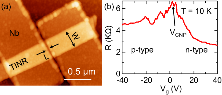
High-quality single crystals of BiSbTeSe2 (BSTS) were grown by the Bridgman technique as described elsewhere Xu et al. (2014); Xu, Miotkowski, and Chen (2016). Devices fabricated on the exfoliated flakes from these crystals exhibit surface dominated conduction with ambipolar field effect, half-integer quantum hall effect, and -Berry phase Xu et al. (2014); Xu, Miotkowski, and Chen (2016). We obtain BSTS nanoribbons using a standard mechanical exfoliation technique and transferred them onto a 500-m thick highly doped Si substrate (used as the back gate) covered with 300-nm SiO2 on top. We locate BSTS nanoribbons, which are randomly dispersed on the substrate, by an optical microscope. An atomic force microscope (AFM) image of a representative JJ is shown in Fig 1a. Multiple electrodes, with electrode separation 100 nm between the adjacent electrodes, are defined by e-beam lithography for each TINR. We then deposit 30-nm thick Nb contacts by a DC sputtering system. A short ( 5 sec) in situ Ar ion milling prior to the metal deposition is used to remove any residues left from the lithography step and native oxides on the TINR surface. Our results presented here are taken from a TINR sample with a thickness of 20 nm, width of 250 nm, and electrode separation of 60 nm.
Fig. 1b depicts vs. the back-gate voltage () at = 10 K (above the critical temperature of our deposited superconductor, 6.5 K). The charge neutrality-point voltage () is 4 V for this device. The electron- and hole-dominated regimes can be easily observed in Fig. 1b as we tune away from the . Using BCS theory, we estimate the = 0 K superconducting gap as = 1.76 975 eV.
When the sample is cooled down below , the electronic transport in the junction is strongly affected by the superconducting proximity effect. The evidences of this effect manifest themselves as the flow of a supercurrent in the junction and the appearance of multiple Andreev reflections (MAR) Tinkham (2004); Xiang et al. (2006). Fig. 2a shows the colormap of the differential resistance () vs. and at = 30 mK. The DC voltage vs. current ( vs. ) characteristic of the junction at = 30 mK for a few different ’s is also presented in Fig. 2b. As we increase from zero, the junction is in its superconducting state and its resistance is zero. However, once is increased above a critical value (, marked by an arrow in Fig 2b), the junction transitions from the superconducting state to a normal state with a non-zero resistance. The junction critical current, , is highlighted by a white curve in Fig. 2a. First, we observe that is gate tunable, with larger for . However, when is tuned near the charge neutrality point ( 4 V), decreases and eventually saturates for more negative ’s as previously observed in Bi2Se3 flakes Cho et al. (2013) and graphene Ben Shalom et al. (2015); Calado et al. (2015). One possible explanation for the saturation of for below the is that the Nb electrodes electron-dope the underlying material (TINR). Therefore, when , a p-n junction is formed in the TINR. This p-n junction can weaken and eventually break the induced superconductivity as was shown in graphene Choi et al. (2013). Another plausible explanation may be the poor injection of the holes into TINR’s by Nb, as will be demonstrated from the low transparency of the contacts for from our analysis of MAR’s (Fig. 3). The inset of Fig. 2b shows the dependence of on the Fermi momentum (), where and is the parallel plate capacitance per unit area of a 300-nm SiO2 ( 12 nF/cm2). For nm-1, we observe varies linearly with , as experimentally demonstrated in ballistic graphene Josephson junctions Mizuno, Nielsen, and Du (2013). We also observe the junction critical temperature (, the temperature below which the junction resistance goes to zero and supercurrent starts to flow in the junction) changes with from = 1.6 K for = 40 V to = 0.7 K for = 10 V. Using BCS theory, we extract the induced superconducting gap () in the TINR as = 242 eV and 106 eV for = 40 V and = 10 V, respectively. We note that the resistance () of the junction does not change as we increase above (V) and even slightly beyond as will be discussed later. As a result, the normal resistance () in our junctions is obtained at slightly above . We obtain 304 V and 266 V for = 40 V and 10 V, respectively.
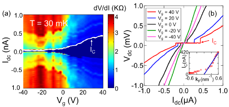
Fig. 3a displays vs. for = 40 V at = 30 mK. Several peaks (within the Nb superconducting gap) in are observed at (where and 13) as marked by the arrows in Fig. 3a. These dI/dV peaks are consistent with MAR Tinkham (2004). We note that these peaks are symmetric around = 0 V and thus below we focus only on the positive peaks. No feature in dI/dV vs. is identified for and is achieved for instead of . The absence of the first () MAR peak has been noted in some SNS junctions Wiedenmann et al. (2016); Xiang et al. (2006) and may be related to the presence of mid-gap zero-energy states as described elsewhere Badiane, Houzet, and Meyer (2011); San-Jose et al. (2013). From the linear fit of dI/dV peaks vs. , we obtain , which is in excellent agreement with the obtained from the BCS theory and 6.5 K. Moreover, the observed dI/dV peaks are reproducible and independent of sweep direction. While we do not observe any dI/dV peaks corresponding to and 8, higher-order peaks ( and 13) are present, a feature that needs further investigation. The observation of the high-order MAR peaks is an indication of high transparency of contacts in our junction.
Fig. 3b depicts the differential conductance (dI/dV, normalized by 1/) vs. (positive) for T = 30 mK at three different ’s. First, we observe that the position of the dI/dV peaks remains relatively constant with , in contrast to the oscillatory behavior of dI/dV peaks around a resonant level in a quantum dot Buitelaar et al. (2003); Jarillo-Herrero, van Dam, and Kouwenhoven (2006). This suggests the absence of localized states in our TINR devices. The high-order dI/dV peaks observed for further indicate that the contacts are highly transparent. However, for , the amplitude of the dI/dV peaks decreases with more negative , e.g. with vanishing peak amplitudes for and 9 at = -40 V (see Fig. 3c). It has been previously reported that in JJs Du, Skachko, and Andrei (2008); Kjærgaard et al. (2017), the MAR peak amplitude depends on the ratio between (superconducting coherence length in the channel) Du, Skachko, and Andrei (2008) and L (channel length), with larger amplitudes for larger /L. For = 40 V, the amplitude of the peak in the normalized dI/dV is 2, indicating L, which is also corroborated with the observation of supercurrent. Fig. 3c shows details of dI/dV vs. curves (at positive side of ) for three characteristic ’s. The vanishing of dI/dV peaks for may be related to the pinning of the Fermi level to the electron-doped regime under the Nb electrodes and hence the formation of p-n junctions for , as has been observed in graphene JJs Ben Shalom et al. (2015); Calado et al. (2015).
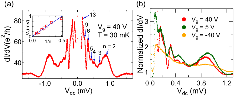
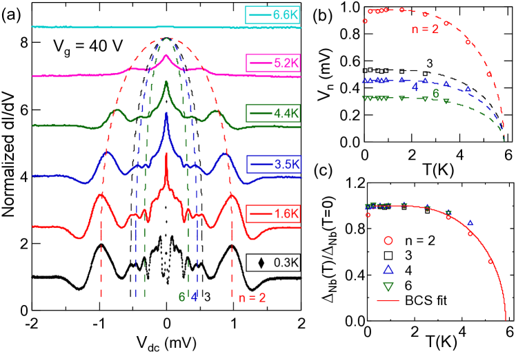
Fig. 4a depicts the T-dependence of the dI/dV (normalized by 1/) vs. for = 40 V, exhibiting a reduction of the Nb superconducting gap with increasing T. Dashed lines are guides to the eyes corresponding to the expected T-dependence of dI/dV peak positions () from BCS theory. We observe a nearly flat and featureless dI/dV vs. for T = 6.6 K (slightly above 6.5 K). We also observe that while dI/dV peaks are noticeable up to high temperatures 5.2 K), the amplitude of the peaks reduces with increasing T, and some of the peaks merge together at higher T (e.g. peaks for and 4 merge at T = 3.5 K). Fig. 4b shows the T-dependence of for and 6. Using the BCS theory to fit vs. T, we extract a 6 K, in fair agreement with 6.5 K. Fig. 4c displays the T-dependence of extracted from each dI/dV peak (for and 6), where , together with the fit of vs. T obtained from the BCS theory, which is seen to describe the data well.
We demonstrated Josephson junctions based on mechanically exfoliated bulk-insulating 3D topological insulator nanoribbons in proximity to superconducting Nb electrodes. We observe high-order ( = 13) multiple Andreev reflections, demonstrating charge transport in the TINR channel is coherent. Furthermore, the critical current exhibits gate effects and can be gate-tuned around one order of magnitude from 50 nA to 430 nA at 30 mK. Our measurements of supercurrent in Josephson junctions based on TINRs help to better understand the nature of induced superconductivity in these junctions and pave the way toward exploration of the envisioned topologically protected devices based on superconductor-TINR-superconductor junctions.
Acknowledgements.
We acknowledge support from NSF (DMR 1410942). The TI material synthesis was supported by DARPA MESO program (Grant N66001-11-1-4107). L.A.J. also acknowledges support by a Purdue Center for Topological Materials fellowship. L.P.R. and A.K. acknowledge support from the U.S. Department of Energy under Award DE-SC0008630.References
- Hasan and Kane (2010) M. Z. Hasan and C. L. Kane, “Colloquium: Topological insulators,” Reviews of Modern Physics 82, 3045–3067 (2010).
- Qi and Zhang (2011) X.-L. Qi and S.-C. Zhang, “Topological insulators and superconductors,” Reviews of Modern Physics 83, 1057–1110 (2011).
- Fu and Kane (2008) L. Fu and C. L. Kane, “Superconducting proximity effect and Majorana fermions at the surface of a topological insulator,” Physical Review Letters 100, 096407 (2008).
- Cook and Franz (2011) A. Cook and M. Franz, “Majorana fermions in a topological-insulator nanowire proximity-coupled to an s-wave superconductor,” Physical Review B 84, 201105 (2011).
- Cook, Vazifeh, and Franz (2012) A. M. Cook, M. M. Vazifeh, and M. Franz, “Stability of Majorana fermions in proximity-coupled topological insulator nanowires,” Physical Review B 86, 1–17 (2012).
- Ilan et al. (2014) R. Ilan, J. H. Bardarson, H. S. Sim, and J. E. Moore, “Detecting perfect transmission in Josephson junctions on the surface of three dimensional topological insulators,” New Journal of Physics 16, 053007 (2014).
- Jauregui et al. (2015) L. A. Jauregui, M. T. Pettes, L. P. Rokhinson, L. Shi, and Y. P. Chen, “Gate tunable relativistic mass and Berry’s phase in topological insulator nanoribbon field effect devices,” Scientific reports 5, 8452 (2015).
- Jauregui et al. (2016) L. A. Jauregui, M. T. Pettes, L. P. Rokhinson, L. Shi, and Y. P. Chen, “Magnetic field-induced helical mode and topological transitions in a topological insulator nanoribbon,” Nature Nanotechnology 11, 345–351 (2016).
- Sacépé et al. (2011) B. Sacépé, J. B. Oostinga, J. Li, A. Ubaldini, N. J. Couto, E. Giannini, and A. F. Morpurgo, “Gate-tuned normal and superconducting transport at the surface of a topological insulator,” Nature Communications 2, 575 (2011).
- Qu et al. (2012) F. Qu, F. Yang, J. Shen, Y. Ding, J. Chen, Z. Ji, G. Liu, J. Fan, X. Jing, C. Yang, and L. Lu, “Strong Superconducting Proximity Effect in Pb-Bi2Te3 Hybrid Structures,” Scientific Reports 2, 339 (2012).
- Veldhorst et al. (2012) M. Veldhorst, M. Snelder, M. Hoek, T. Gang, V. K. Guduru, X. L. Wang, U. Zeitler, W. G. van der Wiel, A. A. Golubov, H. Hilgenkamp, A. Brinkman, V. K. Guduru, U. Zeitler, W. G. v. d. Wiel, A. A. Golubov, H. Hilgenkamp, and A. Brinkman, “Josephson supercurrent through a topological insulator surface state,” Nature materials 11, 417–421 (2012).
- Williams et al. (2012) J. R. Williams, A. J. Bestwick, P. Gallagher, S. S. Hong, Y. Cui, A. S. Bleich, J. G. Analytis, I. R. Fisher, and D. Goldhaber-Gordon, “Unconventional Josephson effect in hybrid superconductor-topological insulator devices,” Physical Review Letters 109, 056803 (2012).
- Sochnikov et al. (2013) I. Sochnikov, A. J. Bestwick, J. R. Williams, T. M. Lippman, I. R. Fisher, D. Goldhaber-Gordon, J. R. Kirtley, and K. A. Moler, “Direct measurement of current-phase relations in superconductor/ topological insulator/ superconductor junctions.” Nano letters 13, 3086−3092 (2013).
- Oostinga et al. (2013) J. B. Oostinga, L. Maier, P. Schüffelgen, D. Knott, C. Ames, C. Brüne, G. Tkachov, H. Buhmann, and L. W. Molenkamp, “Josephson supercurrent through the topological surface states of strained bulk HgTe,” Physical Review X 3, 021007 (2013).
- Finck et al. (2014) A. D. K. Finck, C. Kurter, Y. S. Hor, and D. J. V. Harlingen, “Phase Coherence and Andreev Reflection in Topological Insulator Devices,” Physical Review X 4, 041022 (2014).
- Lee et al. (2014) J. H. Lee, G.-H. Lee, J. Park, J. Lee, S.-G. Nam, Y.-S. Shin, J. S. Kim, and H.-J. Lee, “Local and nonlocal Fraunhofer-like pattern from an edge-stepped topological surface josephson current distribution,” Nano letters 14, 5029–5034 (2014).
- Yang et al. (2014) L. Yang, X. Cui, J. Zhang, K. Wang, M. Shen, S. Zeng, S. a. Dayeh, L. Feng, and B. Xiang, “Lattice strain effects on the optical properties of MoS2 nanosheets.” Scientific reports 4, 5649 (2014).
- Zhang et al. (2011) D. Zhang, J. Wang, A. M. Dasilva, J. S. Lee, H. R. Gutierrez, M. H. W. Chan, J. Jain, and N. Samarth, “Superconducting proximity effect and possible evidence for Pearl vortices in a candidate topological insulator,” Physical Review B 84, 165129 (2011).
- Kurter et al. (2015) C. Kurter, a. D. K. Finck, Y. S. Hor, and D. J. Van Harlingen, “Evidence for an anomalous current-phase relation in topological insulator Josephson junctions,” Nature Communications 6, 7130 (2015).
- Wiedenmann et al. (2016) J. Wiedenmann, E. Bocquillon, R. S. Deacon, S. Hartinger, O. Herrmann, T. M. Klapwijk, L. Maier, C. Ames, C. Brüne, C. Gould, A. Oiwa, K. Ishibashi, S. Tarucha, H. Buhmann, and L. W. Molenkamp, “4-periodic Josephson supercurrent in HgTe-based topological Josephson junctions,” Nature communications 7, 10303 (2016).
- Stehno et al. (2016) M. P. Stehno, V. Orlyanchik, C. D. Nugroho, P. Ghaemi, M. Brahlek, N. Koirala, S. Oh, and D. J. V. Harlingen, “Signature of a topological phase transition in the Josephson supercurrent through a topological insulator,” Physical Review B 93, 035307 (2016).
- Deacon et al. (2017) R. S. Deacon, J. Wiedenmann, E. Bocquillon, F. Domínguez, T. M. Klapwijk, P. Leubner, C. Brüne, E. M. Hankiewicz, S. Tarucha, K. Ishibashi, H. Buhmann, and L. W. Molenkamp, “Josephson Radiation from Gapless Andreev Bound States in HgTe-Based Topological Junctions,” Physical Review X 7, 021011 (2017).
- Xu et al. (2014) Y. Xu, I. Miotkowski, C. Liu, J. Tian, H. Nam, N. Alidoust, J. Hu, C.-K. Shih, M. Z. Hasan, and Y. P. Chen, “Observation of topological surface state quantum Hall effect in an intrinsic three-dimensional topological insulator,” Nature Physics 10, 956–963 (2014).
- Xu, Miotkowski, and Chen (2016) Y. Xu, I. Miotkowski, and Y. P. Chen, “Quantum transport of two-species Dirac fermions in dual-gated three-dimensional topological insulators,” Nat Commun 7, 11434 (2016).
- Tinkham (2004) M. Tinkham, Introduction to superconductivity (Dover Publications, 2004) p. 454.
- Xiang et al. (2006) J. Xiang, A. Vidan, M. Tinkham, R. M. Westervelt, and C. M. Lieber, “Ge/Si nanowire mesoscopic Josephson junctions,” Nature Nanotechnology 1, 208–213 (2006).
- Cho et al. (2013) S. Cho, B. Dellabetta, A. Yang, J. Schneeloch, Z. Xu, T. Valla, G. Gu, M. J. Gilbert, and N. Mason, “Symmetry protected Josephson supercurrents in three-dimensional topological insulators,” Nature Communications 4, 1689 (2013).
- Ben Shalom et al. (2015) M. Ben Shalom, M. J. Zhu, V. I. Fal’ko, A. Mishchenko, A. V. Kretinin, K. S. Novoselov, C. R. Woods, K. Watanabe, T. Taniguchi, A. K. Geim, and J. R. Prance, “Quantum oscillations of the critical current and high-field superconducting proximity in ballistic graphene,” Nature Physics 12, 318–322 (2015).
- Calado et al. (2015) V. E. Calado, S. Goswami, G. Nanda, M. Diez, A. R. Akhmerov, K. Watanabe, T. Taniguchi, T. M. Klapwijk, and L. M. K. Vandersypen, “Ballistic Josephson junctions in edge-contacted graphene,” Nature Nanotechnology 10, 761–765 (2015).
- Choi et al. (2013) J.-H. Choi, G.-H. Lee, S. Park, D. Jeong, J.-O. Lee, H.-S. Sim, Y.-J. Doh, and H.-J. Lee, “Complete gate control of supercurrent in graphene p–n junctions,” Nature Communications 4, 1–10 (2013).
- Mizuno, Nielsen, and Du (2013) N. Mizuno, B. Nielsen, and X. Du, “Ballistic-like supercurrent in suspended graphene Josephson weak links,” Nature Communications 4, 2716 (2013).
- Badiane, Houzet, and Meyer (2011) D. M. Badiane, M. Houzet, and J. S. Meyer, “Nonequilibrium Josephson effect through helical edge states,” Physical Review Letters 107, 177002 (2011).
- San-Jose et al. (2013) P. San-Jose, J. Cayao, E. Prada, and R. Aguado, “Multiple Andreev reflection and critical current in topological superconducting nanowire junctions,” New Journal of Physics 15, 075019 (2013).
- Buitelaar et al. (2003) M. R. Buitelaar, W. Belzig, T. Nussbaumer, B. Babić, C. Bruder, and C. Schönenberger, “Multiple Andreev Reflections in a Carbon Nanotube Quantum Dot,” Physical Review Letters 91, 057005 (2003).
- Jarillo-Herrero, van Dam, and Kouwenhoven (2006) P. Jarillo-Herrero, J. A. van Dam, and L. P. Kouwenhoven, “Quantum supercurrent transistors in carbon nanotubes,” Nature 439, 953–956 (2006).
- Du, Skachko, and Andrei (2008) X. Du, I. Skachko, and E. Y. Andrei, “Josephson current and multiple Andreev reflections in graphene SNS junctions,” Physical Review B 77, 184507 (2008).
- Kjærgaard et al. (2017) M. Kjærgaard, H. J. Suominen, M. Nowak, A. Akhmerov, J. Shabani, C. Palmstrøm, F. Nichele, and C. M. Marcus, “Transparent semiconductor-superconductor interface and induced gap in an epitaxial heterostructure josephson junction,” Physical Review Applied 7, 034029 (2017).