Quantum transport across van der Waals domain walls in bilayer graphene
Abstract
Bilayer graphene can exhibit deformations such that the two graphene sheets are locally detached from each other resulting in a structure consisting of domains with different inter-layer coupling. Here we investigate how the presence of these domains affect the transport properties of bilayer graphene. We derive analytical expressions for the transmission probability, and the corresponding conductance, across walls separating different inter-layer coupling domain. We find that the transmission can exhibit a valley-dependent layer asymmetry and that the domain walls have a considerable effect on the chiral tunnelling properties of the charge carriers. We show that transport measurements allow one to obtain the strength with which the two layers are coupled. We performed numerical calculations for systems with two domain walls and find that the availability of multiple transport channels in bilayer graphene modifies significantly the conductance dependence on inter-layer potential asymmetry.
pacs:
73.20.Mf, 71.45.GM, 71.10.-wI Introduction
A decade ago, researchers started investigating graphene and its associated multilayers for use as a basis for next generation of fast and smart electronic logic gates. The absence of a band gap leads to different proposals for gap generation14-0 ; 14-1 ; 14-2 . For example, by changing the size of the graphene flakes into nanoribbons or quantum dots, one can control the energy gap through size quantization15 ; 15-1 ; 14 . Important experimental advances were achieved in recent years which enabled the fabrication of graphene based electronic devices at the nano scale16 ; 16-1 ; intro-1 .
The increasing control over the structure of graphene flakes allowed for new devices that could constitute the building blocks for a fully integrated carbon based electronics. An example of this is deformed bilayer graphene, where the two layers are not aligned due to a mismatch in orientation or stacking order resulting in e.g. twisted bilayer graphene. Its electronic structure is strongly different from normal bilayer graphene and exhibits very peculiar properties such as the appearance of additional Dirac cones17 ; 18 ; 19 ; 20 ; VanderDonck2016 ; VanderDonck2016b .
Recent experiments have shown that epitaxial graphene can form step-like bilayer/single layer (SL/BL) interfaces or that it is possible to create bilayer graphene flakes that are connected to single layer graphene regions13-1 ; 13-2 ; 20-0 . The appearance of these structures fueled theoretical and experimental investigations on the behavior of massless and massive particles in such junctions. For example, few works have investigated different domain walls that separate, for instance, different type of stackingAB-BA-1 ; AB-BA-2 ; pelc or even different number of layers20-1 ; 22 ; 26 . These theoretical investigations showed that the transmission probabilities through SL/BL interfaces exhibits a valley-dependent asymmetry which could be used for valley-based electronic applications23 ; 24 ; 25 . Other theoretical and experimental works focused on the emergence of Landau levels, edge state properties and peculiar transport properties in such systems27-0 ; 27-1 ; 27-2 ; 27 ; 28 ; 29 ; 30 ; 31 ; 32 ; 33 ; 15 . Bilayer graphene flake sandwiched between two single zigzag or armchair nanoribbons15 ; 34 was also investigated and it was found that the conductance exhibits oscillations for energies larger than the inter-layer coupling.
Most of these recent theoretical works considered domain walls separating patches of bilayer graphene with different stacking type or where only a single layer was connected to a bilayer graphene sheet. Very recently, however, a number of new bilayer graphene platforms have been synthesized. These consist of regions where the coupling between the two graphene layers is changed. For example in the case of folded graphene Wang2017 ; Rode2016 a part of the fold forms a coupled bilayer structure, while another part of it is uncoupledSchmitz2017 ; Hao2016 ; Yan2016 . One has also observed systems with domain walls separating regions of different Bernal stacking Yin2017 ; Yin2016 . In general, these systems can be modelled as being composed of two single layers of graphene (2SL) which are locally bound by van der Waals interaction into an AA- or AB-stacked bilayer structure.
Here, we present a systematic study of electrical transport across domain walls separating regions of different inter-layer coupling. We discuss the dependance on the coupling between the graphene layers, on the distance between subsequent domain walls and on local electrostatic gating. For completeness, we also present all possible combinations of locally detached bilayer systems. Analytical expressions for the transport across a single domain wall are also obtained. These results can serve as a guide for future experiments.
From a theoretical point of view, one can wonder how charge carriers will respond to transitions between systems that have completely different transport properties. For example, single layer graphene and AA-stacked bilayer graphene are known to feature Klein tunnelling at normal incidence while AB-stacked bilayer graphene shows anti-Klein tunnellingKatsnelson2006 ; Stander2009 . It is, therefore, interesting to investigate under which conditions these peculiar chirally-assisted tunnelling properties pertain in combined systems, as well as to investigate how the presence of multiple transport channels changes the transport properties.
From our study we obtain useful analytical expressions for the transmission probability across a single domain wall. These results also show that the effect of local gating is to break the symmetry between the two layers and to introduce a valley-dependent angular asymmetry, which could be used for a layer-dependent valley-filtering device. We show that the inter-layer coupling strength and stacking has a characteristic effect on the conductance across a domain wall which can be used to measure structural deformations in bilayer graphene. We find that the presence of multiple conductance channels in bilayer graphene can modify the dependance of the conductance on an applied inter-layer potential difference from constructive to destructive. Finally, we show that transitions in-between AA-stacked and AB-stacked bilayer graphene systems largely conserve the parity of the transport channel.
The paper is organized as follows. In Sec. II, we discuss the formalism, explain the geometry of the investigated domain walls, and define the possible scattering processes between the different transport modes. In Sec. III, we give analytical expressions for the transmission probabilities through one domain wall and analyze how the symmetry between the graphene layers can be broken by electrostatic potentials. An overview of the numerical results for more complex set-ups consisting of multiple domain walls and gates is presented in Sec. IV. Finally, in Sec. V we briefly summarize the main points of this paper and comment on possible experimental signatures of the presence of coupling domain walls in bilayer graphene.
II Model
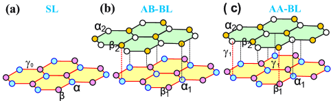
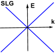
Single layer graphene consists of two inequivalent sublattices, denoted as and , with interatomic distance nm and that are coupled in the tight binding (TB) formalism by eV1 . It has a gapless energy spectrum with band crossings at the so-called Dirac points and that are located at the corners of the Brillouin zone. The energy dispersion around one of these points is depicted in Fig. 1(a).
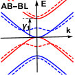
Bilayer graphene consists of two single layers of graphene which can be stacked in two stable configurations: AB-stacked bilayer graphene (AB-BL) or AA-stacked bilayer graphene (AA-BL). In AB-BL, atom is placed directly above atom with inter-layer coupling eVli2009band as shown in Fig. 1(b). It has a parabolic dispersion relation with four bands. Two of them touch at zero energy, whereas the other two bands are split away by an energy . The skew hopping parameters and between the other two sublattices are negligible since they have insignificant effect on the transmission probabilities and band structure at high energies Ben .
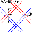
In AA-BL two single layers of graphene are placed exactly on top of each other such that the structure becomes mirror-symmetric. Atoms and in the top layer are located directly above atoms and in the bottom layer, with direct inter-layer coupling AA-gamma1 , see Fig. 1(c). AA-BL has a linear energy spectrum with two Dirac cones shifted in energy by an amount of as depicted in Fig. 1(c) by the full curves.
II.1 Geometries
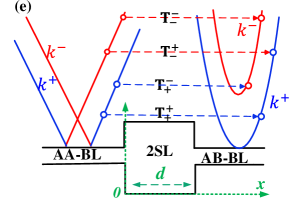
We consider four different junctions that can be made of from the building blocks depicted in Fig. 1: monolayer, AA- stacked and AB-stacked bilayer graphene. Without loss of generality, we assume that the charge carriers are always propagating from the left to the right hand side. Then we consider three different configurations: () a structure where the leads on the left () and on the right hand side () consist of two decoupled single layers while in between they are connected into an AB-BL (AA-BL) configuration. This is depicted in Fig. 2(a). We will refer to such a structure as 2SL-AB-2SL (2SL-AA-2SL). () A structure where the middle region is made up of two decoupled monolayers and whose leads are AB (AA) stacked bilayer graphene. This is depicted in Figs. 2(b, d). Such a configuration henceforth will be refereed to as AB-2SL-AB (AA-2SL-AA). () A structure where a domain wall separates an AB (AA) stacked structure from two decoupled single layers. We will assign the abbreviation 2SL-AB (2SL-AA) to this structure if the charge carriers are incident on one of the two separated layers or AB-2SL (AA-2SL) if the coupled bilayer structure is connected to the source. This is depicted in Fig. 2(c). (IV) left and right leads are bilayer graphene with AA- and AB stacking, respectively, separated by a domain where the two layers are completely decoupled (AA-2SL-AB), see Fig. 2(e). To describe transport in the above mentioned structures, we allow for scattering between the layers as well as between the different propagating modes in an AB-BL or between the two Dirac cones in AA-BL. In the next section, we describe the transport modes in 2SL and BL and how charge carriers can be scattered in-between them.
II.2 Scattering definitions
In this section we define the model Hamiltonian that describes the different structures. For this purpose we use a suitable basis defined by whose elements refer to the sublattices in each layer. The general form of the Hamiltonian near the K-point reads
| (1) |
The coupling between the two graphene layers is controlled by the parameters and through which we can “switch on” or “switch off” the inter-layer hopping between specific sublattices. This allows to model different stackings by assigning different values to these parameters. For , the two layers are decoupled and the Hamiltonian reduces to two independent SL sheets. To achieve AA-stacking we select and while for AB-stacking we need and . In Eq. (1) m/s is the Fermi velocity1 of charge carriers in each graphene layer, denotes the momentum, and are the potentials on layers 1 and 2. In the present study, we only apply these potentials in the intermediate region. We assume that the domain wall is oriented in the -direction and of infinite length. Therefore, the system is translational invariant and the momentum is conserved. This enables us to write the wave function as .
II.2.1 Decoupled graphene layers
The eigenfunctions of the 2SL Hamiltonian are those of the isolated graphene sheet, 1
| (2) |
where is the layer index, with sgn, , . Introducing the length scale , which represents the inter-layer coupling length, allows us to define the following dimensionless quantities:
| (3) |
Notice that for the two stacking configurations, was found to be different. For the AB-BL the value is eV while for AA-BL it is eVli2009band ; AA-gamma1 ; AA-Yuehua2010 .
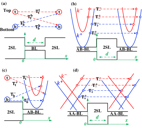
In order to discuss the different scattering modes, we introduce the notation , where can stand for transmission () or reflection () probabilities and the indexes denote the mode by which the particles are incoming or outgoing. Fig. 2 depicts all possible transitions that are considered in the present work. Fig. 2(a) shows all possible transmission processes in a 2SL-BL-2SL system where denotes the top layer on either side and the bottom layer. For example, denotes a particle coming through the top layer and exiting on the bottom layer.
II.2.2 AB-stacking
For AB-BL there are two branches corresponding to propagating modes. These branches correspond to the wave vector given by
| (4) |
The modes presented in Eq. (4) labeled by “” correspond to eigenstates that are odd under layer inversion, while the “”modes are even. These modes are shown, respectively, in blue and red in Fig. 2(b). This means that there are two available channels for transmission at a given energy, and an additional two for the reflection probabilities. Note that for energies , there is only one propagating mode and one transmission and reflection channel. Similarly, the wave function of AB-BL can be written as Ben
| (5) |
where corresponds to a diagonal matrix consisting of exponential terms, while the components of the constant vector depend on the propagating region, and is given by
| (6) |
where and .
The use of the matrix notation will prove to be very useful to construct the transfer matrix as outlined below.
II.2.3 AA-stacking
In the case of an AA-BL, the corresponding wave function can be written similar to Eq. (5) but now with the matrix given by
| (7) |
where , and ). To investigate when scattering between the Dirac cones of AA-BL is allowed or forbidden, one can apply a unitary transformation that forms symmetric and anti-symmetric combinations of the top and bottom layer. This yields a Hamiltonian in the basis of the form:
| (8) |
For , this Hamiltonian is block-diagonal and represents two Dirac cones as shown in Fig. 1(c). The two cones correspond to modes with wave vector given by
| (9) |
In Fig. 1(c) the blue bands corresond to the odd modes and red bands, denoting the even modes, are given by the wavevector. In these equations, denotes the energy shift of the whole spectrum. This shift can be chosen zero by assigning the same magnitude but different signs to the electrostatic potentials on both layers . Eq. (8) shows that for zero electric field () both cones are decoupled and the scattering between them is strictly forbidden. This was used before in Ref. [AA-cones, ] to propose AA-BL as a potential candidate for “cone-tronics” based devices. However, this protected cone transport is broken for finite bias () and hence scattering between the cones is allowed. Furthermore, one might wonder if the charge carriers stay within their cone transport through a domain consisting of two decoupled layers.
II.2.4 Scattering probability
In order to calculate the scattering probability in the reflection and transmission channel, we use the transfer matrix method together with boundary conditions that require the eigenfunctions in each domain to be continious for each sublattice Barbier ; Ben2 . To conserve probability current we normalize transmission probabilities and reflection probabilities such that
| (10) |
where, the index refers to the incoming mode while the index denotes the outgoing mode. For a coupled bilayer the different modes are labelled by “” for the modes that are even under in-plane inversion and by “” for odd modes. For a decoupled 2SL system, we employ the notation for the top layer and for the bottom layer. For example, for the system 2SL-AB-2SL and for an incident particle in the top layer of 2SL gives . In Fig. 2 all possible transition probabilities are shown schematically.
II.2.5 Conductance
To obtain measureable quantities, we finally calculate the zero temperature conductance that can be obtained from the Landauer-Büttiker formula Landauer where we have to sum over all the transmission channels,
| (11) |
with the length of the sample in the -direction and . The factor comes from the valley and spin degeneracy in graphene. The total conductance of any configuration is the sum of all available channels .
III Transmission across a single domain wall
Here we will present analytical expressions for the transmission probabilities of transport across a single domain wall. These analytical expressions will shed light on the requirements for transport across a domain wall and how local electrostatic gating can affect these transport properties. By doing so, we encounter that curiously, electrostatic gates can break the symmetry between the layers in the transmission probability if there are evanescent modes in the system. The breaking of the layer symmetry results in an asymmetric angular distribution of the transmission probability as will be shown further.
We consider a situation where two propagating modes exist in the AB-BL or AA-BL. This requires some caution in defining the incident angle in the calculation of the transmission probabilities. Failing to do so may result in erroneous results such as transmission exceeding unity or unexpected symmetry featureskumar ; Ben03 . Considering one domain wall, the simplest configuration, separating 2SL and either AA or AB-BL allows to obtain analytic expressions for the transmission probabilities. The incident angle for each propagating mode depends on the type of layer stacking in the incident region. Hence, for charge carriers incident from 2SL we define
| (12) |
On the other hand, when charge carriers are incident from AB-BL we need to define incident angle for each mode separately such that
| (13) |
Finally, if charge carriers incident from AA-BL the associated angle is defined as
| (14) |
A straightforward calculation results in the transmission probability for charge carriers incident from 2SL and impinging on AA-BL
| (15) |
while for the reverse configuration (AA-2SL) it is given by
| (16) |
Similar as performed for the AA-BL Hamiltonian, also the AB-BL Hamiltonian can be expressed in terms of symmetric and anti-symmetric combinations of the two layers. This manipulation allows to determine a closed-form expression for the transmission probability of the 2SL-AB structure. The derivation is outlined in Appendix A and results in
| (17) |
with and for . For the reverse configuration (AB-2SL) the transmission probabilities are
| (18) |
where , and are functions defined in Appendix A.
For a domain wall separating 2SL and AA-BL, the transmission probabilities are always symmetric with respect to normal incidence as indicated in Eqs. (15,16). In other words, for the 2SL-AA and similarly for AA-2SL configuration, and this symmetry still holds when the right side of the junction is gated (). We will refer to this symmetry as “layer symmetry” since it is a consequence of the equivalence of 2SL layers and the symmetric coupling of the AA-BL.
Notice that Klein tunnelling for normal incidence in SL and AA-BL is also conserved in the combined structure. For example, in 2SL-AA and for normal incidence (), the modes become and hence Eq. (15) reads Then, for charge carriers propagating in the bottom (top) layer it may be transmitted into or states and thus the total probability is . As a result of Klein tunnelling at normal incidence, the corresponding reflection probabilities are zero such that . In an analogous manner it can be shown that for normal incidence Eq. (16) gives
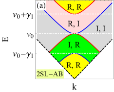
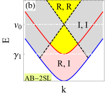
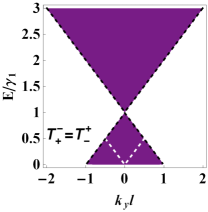
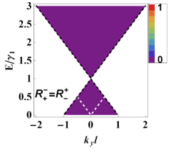
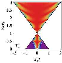
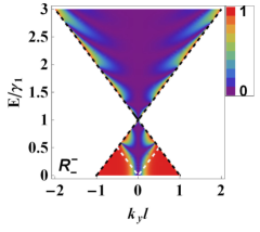
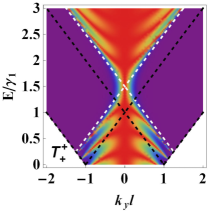
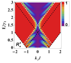
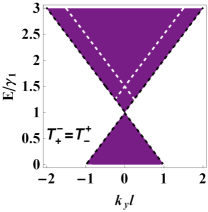
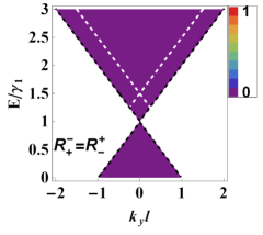
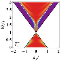
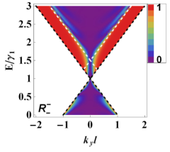
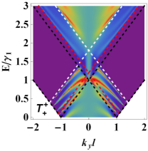
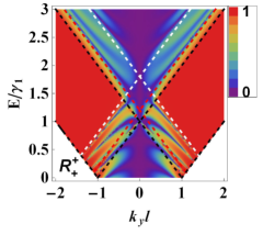
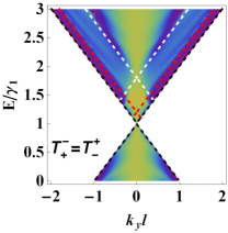
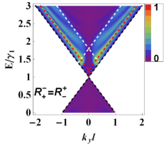
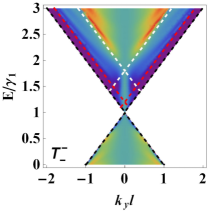
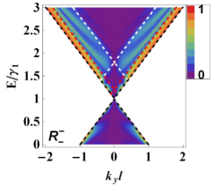
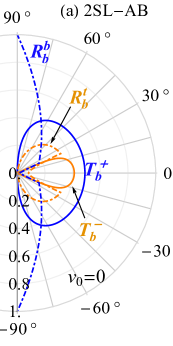
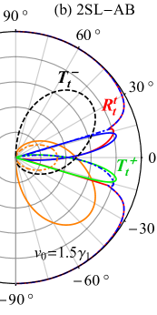
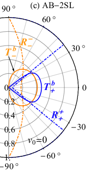
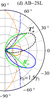
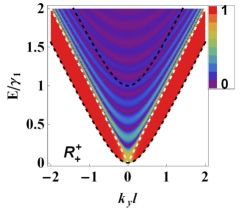
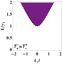
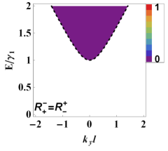
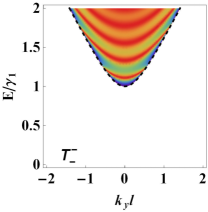
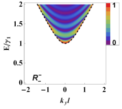
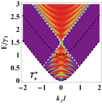
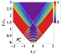
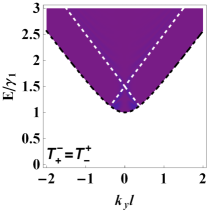
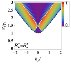
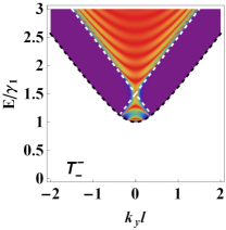
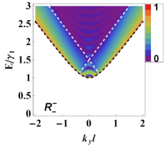
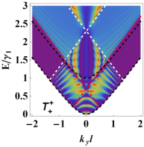
Turning now to the 2SL-AB/AB-2SL case, one can infer from Eqs. (17,18) that for the layer symmetry holds since the only term carrying asymmetric features is proportional to . However, for it is striking that despite the fact that a homogeneous electrostatic potential does not break any in-plane symmetry in the system, layer symmetry is broken. This leads to an angular asymmetry in the transmission channel, i.e. for 2SL-AB and for AB-2SL. Upon further analysis of Eqs. (17,18), one notices that this asymmetric feature is present in regions in the () plane where one of the two modes is propagating while the other is evanescent. In Figs. 3(a,b) we show a diagram for these different regions associated with 2SL-AB and AB-2SL, respectively. The layer symmetry is broken in the green and pink regions while in the yellow regions layer symmetry holds.
The mechanism for breaking the layer symmetry in configurations consisting of AB-BL is attributed only to the evanescent modes. For example, in 2SL-AB (see Fig. 3) the transmission probability for charge carriers to be transmitted into from either bottom or top layers of 2SL is
| (19) |
where . The above equation shows that layer symmetry is broken, only when and which is satisfied in the pink and gray regions in Fig. 3(a). However in the gray region there are no propagating states and consequently the transmission probabilities are zero. The same analysis applies also to where the asymmetric feature is preserved only when as shown by the green region in Fig. 3(a). For AB-2SL configuration, the layer asymmetry is only reflected in the , see Eq. (18), since corresponds to the pink region in Fig. 3(b). While for , the propagating states are only available for (yellow region in Fig. 3(b)) which coincides with . Thus, the layer symmetry is always conserved in as it can be seen in Eq. (18). Now it is clear why layer symmetry is not broken in the AA-BL configuration; because there are always two propagating modes associated with any energy value.
The breaking of angular symmetry in this situation is qualitatively similar to that obtained in AB-BLBen subject to an inter-layer bias. One can connect this layer asymmetry in the vicinity of the two valleys and through time-reversal symmetry. The Hamiltonian can be related to the Hamiltonian through the transformation
| (20) |
where is the time-reversal symmetry operator. This implies, for example in the channel, that charge carriers moving from right to left and scattered from the bottom layer to in valley are equivalent to those scattered from top layer to but moving in the opposite direction in the vicinity of . If layer symmetry holds in the vicinity of one of the valleys, then the transmission probabilities of charge carriers moving in the opposite directions must be the same. It is worth pointing out here that the layer asymmetry in the valley is reversed in the valley and hence the overall symmetry of the system is restored. Therefore, the macroscopic time reversal symmetry is preserved.
IV Numerical Results
We first present the results for transmission, and reflection probabilities and for the conductance in the case of domain walls separating 2SL and AA-BL structures. The different regions as defined in Fig. 3 are superimposed as dashed black and white curves. Moreover, in calculating the transport properties we considered different magnitudes for the electrostatic potential and bias applied to the drain structure.
IV.1 AA-Stacking
IV.1.1 2SL-AA/AA-2SL
We consider charge carriers tunnelling through 2SL-AA and AA-2SL systems. In Fig. 4(a) we show the transmission and reflection probabilities for charge carriers impinging on pristine AA-BL as a function of incident angle . As a result of the layer symmetry, charge carriers incident from bottom/top layer of 2SL and transmitted into the lower Dirac cone () in the AA-BL will have the same transmission probability . Similarly, for those charge carriers transmitted into the upper cone, they will also have the same probability regardless which layer they are incident from.
This symmetry stems from the fact that the wavefunction in the 2SL are a superposition of two spinors corresponding to the two sublattices while in AA-BL it is a superposition of four. For this reason, charge carriers incident from top or bottom layer of 2SL have the same dynamics and hence share their transmission probability. A partial reflection into the same layer, is shown in Fig. 4(a), which corresponds to evanescent modes associated with the upper Dirac cone (). As in transmission, charge carriers can be back scattered between the layers. However, the absence of the electrostatic potential results in a small scattering current as depicted in Fig. 4(a). In addition, scattering back from top to bottom layer or vice versa occurs also with the same reflection probabilities .
Because of chiral decoupling of oppositely propagating waves in AA-BL and in SL, back-scattering is forbidden for normal incidence () and thus the reflection probabilities for each channel are zero, i.e. . This is associated with perfect tunnelling . The effect holds for all forthcoming structures composed of AA-BL and 2SL.
Fig. 4(b) shows the numerical results of the same system, 2SL-AA, but now in the AA region, the potential is increased to . This shifts the two Dirac cones in energy to . As a result of the presence of the electrostatic potential, a strong scattered reflection takes place when there are no propagating modes in the AA section.
In Figs. 4(c,d), we show the reversed configuration, i.e. an AA-2SL system. The transmission and reflection probabilities for zero () and with nonzero () electrostatic potentials applied to 2SL are reported in panels (c) and (d) respectively. Similar to the 2SL-AA system, we can note that layer symmetry still holds such that and . Furthermore, we find strong non-scattered reflection in the and channels that is associated with evanescent modes on both sides of AA-BL and 2SL whereas the scattered reflection channels and are always zero due to the protected cone transport discussed earlier.
IV.1.2 2SL-AA-2SL
In this Section, we show the results of transport across two domain walls forming a system with three regions; where AA-BL is sandwiched between two regions of 2SL, see Fig. 2(a). Such a system can exhibit a strong layer selectivity when current flows through the intermediate region , i.e. AA-BL. This behaviour has already been investigated in Ref. [Hasan1, ]. Here, however, we go in much more detail to show how the different transmission and reflection channels are affected by the electrostatic potential or finite bias applied to the intermediate region.
In Figs. 5 and 6 we show the scattered and non-scattered channels for transmission and reflection for pristine AA-BL and with electrostatic potential of strength , respectively. Layer symmetry is preserved in both reflection and transmission channels as clarified in Figs. 5. and 6 also show strong scattered transmission, especially for normal incidence which can be altered depending on the width of the AA-BL. When an electrostatic potential is applied to the middle domain, resonances appear in the transmission probabilities for as shown in Fig. 6. This is a consequence of the finite size of the AA-BL and the presence of charge carriers with different chirality in the mentioned range of energies AA-cones . Introducing a finite bias on AA-BL breaks the layer symmetry of the system. As a result, and . However, it is still preserved in the scattered channels and ( see Fig. 7).
It is worth mentioning here that the finite bias does not break the angular symmetry with respect to normal incidence in the transmission and reflection probabilities as it does for normal AB-BLBen . This is a manifestation of the symmetric inter-layer coupling in AA-BL.
IV.1.3 AA-2SL-AA
In this system we interchange the AA-BL and 2SL as shown in Fig. 2(d). In this case, scattering is defined between the two cones in the AA-BL regions. In Figs. 8 and 9 we show the transmission and reflection probabilities between the two Dirac cones through the pristine 2SL and in the presence of an electrostatic potential, respectively. The first and the last rows of Figs. (8) and (9) show the non-scattered transmission and reflection probabilities corresponding to the lower and upper Dirac cones, respectively. We notice that Klein tunnelling is preserved at normal incidence. This shows that Klein tunnelling in AA-stacked bilayer graphene is a robust feature that is insensitive to local changes in the inter-layer coupling. On the other hand we see that scattering between two different Dirac cones remains strictly forbidden even with a local decoupling of the two layers. Therefore, these devices could be used for conetronics. As a result, in the second row of Figs. 8 and 9 the scattered transmission and reflection channels are zero .
In Fig. 10 we plot the transmission and reflection probabilities for a potential strength and inter-layer bias . The shift in the bands of the top (white) and bottom (red) layer of 2SL is due to the inter-layer bias which couples the two Dirac cones as shown in Eq. (8).
Therefore, the suppression of the scattering transmission and reflection probabilities due to the protected cone transport does not hold anymore. It is, therefore, possible that scattering between different cones takes place as clarified in the second row of Fig. 10.
IV.1.4 Conductance
The conductance of two and three-block systems is shown in Figs. 11 and 12, respectively. For the two systems 2SL-AA and AA-2SL with pristine AA-BL and 2SL, the conductance for different channels is shown in Figs. 11(a, b). It shows that the conductance of these two systems are identical. Referring to Figs. 4(a, c) we notice that the transmission probabilities for pristine 2SL-AA and AA-2SL are quite different. However, the corresponding conductances (see Fig. 11) exhibit time reversal symmetry in spite of the fact that the domain wall separates two different systems. This is a strong point which can be verified experimentally even in the case of zero electrostatic potential.
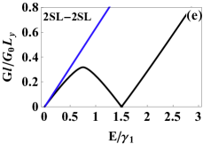
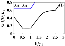
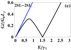
Adding an electrostatic potential to one of the two sides leads to different behavior in the conductance of the above mentioned two systems as depicted in Figs. 11(c,d). In Fig. 11(c) the charge carriers incident from 2SL and impinging on AA-BL whose bands are shifted by . Each conductance channel gives zero at due to the absence of propagating states in the 2SL at this energy, even though there are propagating states available in AA-BL corresponding to two cones. We note also that are almost zero at upper and lower cones as a result of the absence of states at these points as seen in Fig. 11(c). In Fig. 11(d) we see that the conductance of different channels is not zero in contrast to the previous case because here at there are propagating states available in both AA-BL and 2SL. Furthermore, all channels have one minimum, due to the lack of states, at which corresponds to the Dirac cone in 2SL shifted by while has also another minimum at the upper cone as shown in Fig. 11(d). Finally, for comparison we add in Figs. 11(e, f) the conductance that will be measured in the absence of a domain wall for 2SL-2SL and AA-AA junctions with (blue curves). Our results indicate that domain walls are experimentally identifiable channels even in the absence of a gate. As a reference we also calculate the total conductance in the presence of an electrostatic potential () as shown with black curves in Figs. 11(e, f) which corresponds, in this case, to the usual p-n junctions in single-layer graphene and AA-BL, respectively.
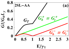
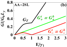
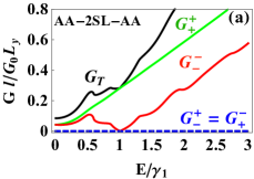
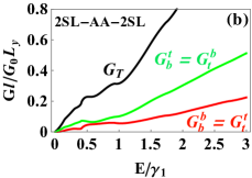
The conductance of three-block systems is shown in Fig. 12 where left and right panels correspond to AA-2SL-AA and 2SL-AA-2SL structure, respectively. Protected cone transport leads to zero conductance in the scattered channels as shown in Fig. 12(a). A close inspection also reveals that at with finite and non-zero values, regardless of the fact that in the 2SL region there are no available propagating states. This is attributed to the evanescent modes in 2SL at which are responsible for ballistic transport in grapheneSnyman . We thus also expect that (red curve in Fig. 12(a)) should be exactly zero at the Dirac cone as a result of the absence of propagating states in the leads at this energy.
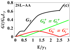
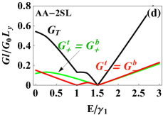
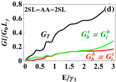
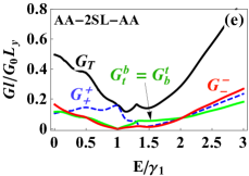
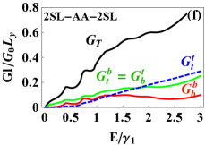
By shifting the bands of 2SL using a local potential with strength , a local minimum appears in the conductance at which corresponds to the position of the charge-neutrality point in 2SL as shown in Fig. 12(c). This minimum can be obtained by aligning the upper cone in AA-BL and the Dirac cone in 2SL such that they are located at the same energy, this can be achieved by choosing . The main difference introduced by applying an inter-layer bias is the broken protected cone transport where now as depicted in Fig. 12(e). For completeness, we performed similar calculations but now with 2SL as the leads (2SL-AA-2SL) and the results for the conductance with pristine, gated and biased AA-BL are shown in Figs. 12(b, d, f), respectively. Here, all conductance channels are zero at such that and as shown in Figs. 12(b, d). Similarly, the main features in Fig. 12(f) are in qualitative agreement with those shown in Figs. 12(b, d) but now the tunnelling equivalence through the same channel is broken so that . This is a direct consequence of the perpendicular electric field which leads to the breaking of the inter-layer sublattice equivalence. The peaks appearing in the total conductance are due to the finite size of the AA-BL region.
IV.2 AB-Stacking
IV.2.1 2SL-AB/AB-2SL
In this section, we evaluate how the stacking of the connected region changes the transport properties across a domain wall. The angle-dependent transmission and reflection probabilities for pristine systems 2SL-AB are plotted in Fig. 13(a). The charge carriers can be incident from the two layers in the 2SL structure and impinge on AB-BL where, depending on their energy, they can access only one propagating mode or two if the energy is large enough. Scattering from the top or bottom layer of 2SL into one of these modes is equivalent as well as backscattering and hence, as before, layer symmetry is preserved (see Fig. 13(a)). In Fig. 13(b) we show results with the AB-BL region subjected to an electrostatic potential of strength . Surprisingly, we see that the layer symmetry is broken and an asymmetric feature with respect to normal incidence shows up in the transmission and non-scattered reflection probabilities, see Appendix A, such that For example, as well as the non-scattered reflection channels as discussed in Sec. III. This asymmetric feature can be understood by resorting to the bands on both sides of the junction, where due to the electrostatic potential the band alignment of 2SL and AB-BL is altered. In this case, the center of the AB-BL band is shifted upwards in energy with respect to the crossing of the 2SL34 energy bands. The origin of such asymmetry is a direct consequence of the asymmetric coupling in AB-BL which leads to shifting of the bands by . Therefore, at low energy there is only one propagating mode (i.e one type of charge carrier ) and consequently only is available. For larger energy, on the other hand, there are two modes available giving rise to four channels .
The angular asymmetry feature is present only in the region in the -plane where there is only one propagating mode. This can be also understood as a manifestation of the asymmetric amplitude of the wave function in the AB-BL side due to the evanescent modes in this region 24 . The theory of tunnelling through an interface of monolayer and bilayer was presented earlier24 and such asymmetry was noticed as well. Moreover, in our case there are two single layer graphene sheets connected to the bottom and top layers of the bilayer system but the asymmetric feature in Ref. [24, ] will be recovered when considering only one propagation channel. For instance, the transmission probabilities and presented in Fig. 13(b) show the same asymmetric features discussed in Ref. [24, ]. This asymmetry feature is reversed in the other valley, so that the total transmission or reflection averaged over both layers is symmetric as can be seen from Fig. 13(b). However, this valley-dependent angular asymmetry could also be used for the basis of a layer-dependent valley-filtering device as proposed in other worksCosta2015 ; Rycerz2007 .
The above analogy, which is discriminating between the presence of one or two modes, applies also to the non-scattered reflection probabilities and . These non-scattered currents are carried by the states localized on the disconnected sublattices and , as seen in Fig. 1. In that case, there is one traveling modepelc and thus, inherently, a layer asymmetric feature will be present. In contrast, for the scattered channels and the charge carriers must jump between the layers of AB-BL. This occurs through the localized states on the connected sublattices and where there are two travelling modes and, hence, these probabilities exhibit layer symmetry as shown in Fig. 13(b). In the AB-2SL configuration, where charge carriers incident from the AB-BL impinge on the 2SL, we show the angle-dependent transmission and reflection probabilities in Fig. 13(c) for pristine 2SL and AB-BL.
Similar to the previous configuration 2SL-AB, the results are symmetric in this case because the Dirac cones of both systems (2SL and AB-BL) are aligned. Furthermore, there is an equivalence in the transmission channels such that with partial reflection associated with the non-scattered channels and . While for the scattered channels and are almost zero. This is due to efficient transmission resulting from the absence of the electrostatic potential in the 2SL. An electrostatic potential of strength induces a scattering between the two modes in the reflection channels so that now as depicted in Fig. 13(d). In addition, it breaks the band alignment and gives rise to the layer asymmetry feature in the transmission probabilities where only one travelling mode exists i.e. . Thus, always preserves layer symmetry in this case, see Fig. 13(d), because the mode exists for where also the mode is available as discussed above. This is also the same reason that configurations consisting of AA-BL always preserve layer symmetry. Indeed, AA-BL does not have a region in the -plane with only one propagating mode, and there are always two travelling modes for all energies.
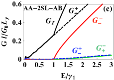
IV.2.2 2SL-AB-2SL
Different configurations have been proposed to connect a single layer to the AB-stacked bilayer graphene25 ; 34 ; 15 ; Lima . Now, two SL are connected to the AB-stacked bilayer, see Fig. 2(a). In Fig. 14 we show the dependence of the transmission and reflection probabilities on the transverse wave vector and the Fermi energy. It appears that all channels are symmetric with respect to normal incidence since the Dirac cones of AB and 2SL are aligned. It also implies that scattered and non-scattered channels of the transmission and reflection are equivalent such that and (see Fig. 14).

Another interesting feature of this configuration is that for the scattered and non-scattered transmissions are equal . In this energy regime such device can be used as an electronic beam splitterBrand ; Lima .
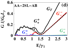
Fig. 15 displays the same plot as in Fig. 14 but with an electrostatic potential on the AB-BL region. There is an important difference as compared to the pristine AB-BL case, the layer symmetry is broken such that as clarified in Fig. 15. This can be also understood by pointing out that charge carriers scattered from top to bottom when moving from left to right in the valley are equivalent to charge carriers scattering from bottom to top when moving oppositely in the second valley .
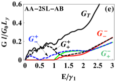
Introducing a finite bias () to the AB-BL region along with an electrostatic potential () will shift the bands and opens a gap in the spectrum. As a result of the presence of a strong electric field, the transmission channels are completely suppressed inside the gap due to the absence of traveling modes as seen in Fig. 16. Moreover, non-zero asymmetric reflection appears in the gap as well as a violation of the equivalence of non-scattered transmission channels. This is a result of the breaking of inter-layer sublattice equivalence Ben . In addition, some localized states appear inside the “Mexican hat” of the low energy bands where they are pushed by the strong electric field (), see Fig. 16.
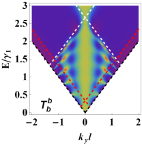
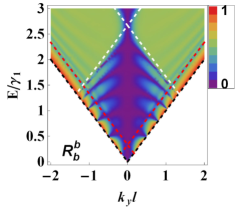
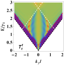
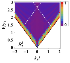
There is a link between the transmission probabilities of our system 2SL-AB-2SL and those investigated by González et al. 34 . The channels and are qualitatively equivalent to those obtained in Ref. [34, ]. For example, shows electron-hole () and symmetry whereas exhibits another symmetry which can be obtained under the exchange . The results in Fig. 17 are in good agreement with those of Ref. [34, ] where we fix and nm.
IV.2.3 AB-2SL-AB
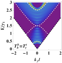
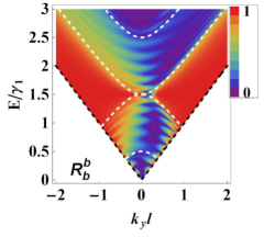
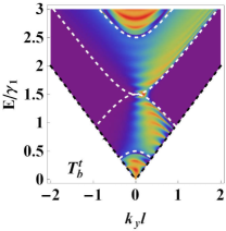
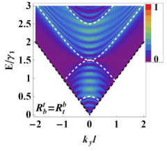
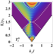
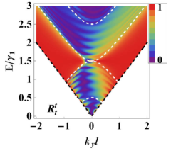
For leads composed of AB-BL where the intermediate region is pristine 2SL, we show the results in Fig. 18 for the transmission and reflection probabilities. Now charge carriers will scatter between the different modes of the AB-BL on the left and right leads as shown in Fig. 2(b). As expected, all channels are symmetric and as a result of the finite size of the 2SL region, resonances appear in as shown in Fig. 18. These so-called Fabry-Pérot resonances appear at quantized energy levelsmasir2010
| (21) |
This is the dispersion relation for modes confined in the 2SL region with width .
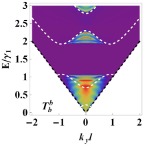
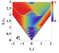
The results presented in Fig. 18 reveal no scattering between the two modes and and charge carriers are only transmitted or reflected through the same channel from which they come from. Unexpectedly, introducing an electrostatic potential induces a strong scattering in the reflection channels () and very weak scattering in the transmission channels (), as seen in Fig. 19. When the 2SL are biased, the Dirac cones at bottom and top layers will be shifted up (white dashed lines) and down (red dashed lines) in energy, respectively (see Fig. 20). This bias will strengthen the coupling between the two modes resulting in a strong scattering between them. In addition, the inversion symmetry is broken due to the bias leading to an asymmetry with respect to normal incidence.
IV.2.4 Conductance

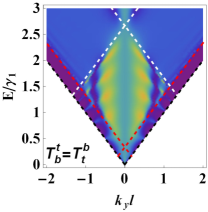
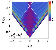
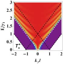
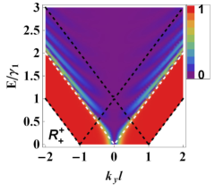
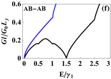
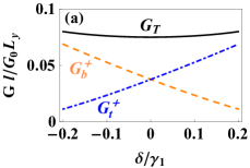
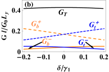
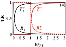
The conductance of the two-block system consisting of 2SL and BA-BL is shown in Fig. 21 for different values of the applied gate voltage. Figs. 21(a,b) reveal that the system where charge carriers are incident from the 2SL and impinge on AB-BL and vice versa are equivalent to the case when both 2SL and AB-BL are at the same potential. As seen in Figs. 21(a,b), are contributing to the total conductance starting from where the mode exists. On the contrary, only contributes when where states are available and this appears as a sharp increase in at . On the other hand, considering an applied electrostatic potential on the right side of the two-block system will break this equivalence as seen in Figs. 21(c,d). In addition, as a result of the shift of the Dirac cone in AB-BL (see Fig. 21(c)) or 2SL (see Fig. 21(d)) due to the electrostatic potential, all conductance channels are zero at . Similar to the AA-BL case, the conductances of the pristine systems 2SL-AB/AB-2SL (see Figs. 21(a, b)) clearly preserve the time reversal symmetry. Even though, both systems have different transmission probabilities as can be seen from Figs. 13(a, c). We also show in Figs. 21(e, f) the total conductance in the absence of domain wall in 2SL-SL and AB-AB systems, respectively, for (blue curves) and (black curves). This shows that transport channels in the presence of domain walls are experimentally recognisable.
In Fig. 22 we show the conductance in a 2SL-AB system as a function of the bias for transport using a single Fig. 22(a) or a double Fig. 22(b) mode. The results show that the contribution from the top and bottom layers to the conductances have opposite behaviours as a function of the inter-layer bias. The total conductance , however, has a convex form, increasing with the application of an inter-layer bias. From Fig. 22(b), on the other hand, we see that when a second mode is available, four channels contribute to the conductance and the total conductance assumes a concave form, i.e. decreasing with increasing inter-layer bias. This is a characteristic experimental feature that can signal the presence of a second mode of propagation.
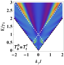
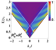
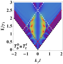
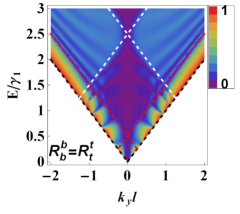
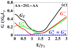
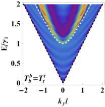
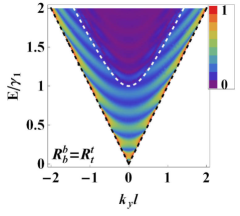
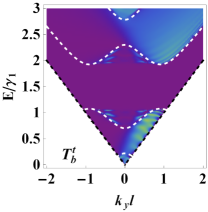
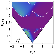
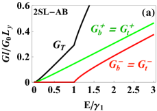
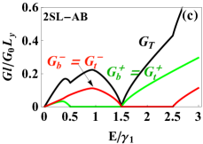
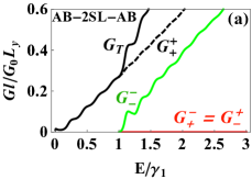
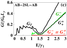
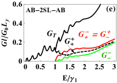
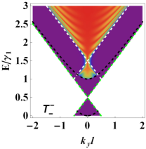
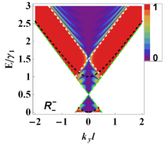
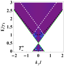
For the three-block system we show the conductance of the configuration AB-2SL-AB and 2SL-AB-2SL in the left and right columns of Fig. 23, respectively. The resulting conductance of the first configuration shows only two non-zero channels and , while the scattered ones since (see Fig. 23(a)). Furthermore, for low energy since the mode is not available in this regime but it starts conducting when . The applied electrostatic potential on the 2SL keeps the scattered conductance channels at zero and a minimum in the conductance appears around the shifted Dirac cone of the 2SL as depicted in Fig. 23(c). As pointed out before, if the Fermi energy approaches the strength of the electrostatic potential, a non-zero minimum is present in the conductance because charge carriers can be transmitted through a width of 2SL via evanescent modesSnyman . In Fig. 23(f) this minimum disappears and the conductance dramatically increases at . This is because the bias will couple the two modes and two additional scattered channels and start conducting. The resonant peaks resulting in the conductance, see Figs. 23(a,c,e), are due to the finite size of the intermediate region and hence strictly depend on its width .

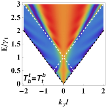
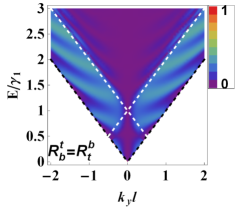
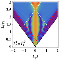
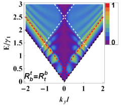
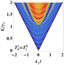
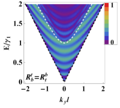
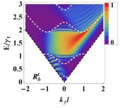
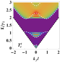
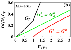
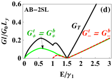
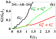
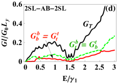
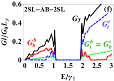
On the other hand, the conductance of the configuration 2SL-AB-2SL has different features. In Fig. 23(b) the four channels, in contrast to the previous configuration, start conducting from . This possess layer symmetry such that and . Of particular importance is the equivalence of the four channels for while for charge carriers strongly scatter between the layers () as shown in Fig. 23(b). This equivalence of the four channels in the regime vanishes when an electrostatic potential is applied () to the intermediate region as seen in Fig. 23(d). However, the scattered and non-scattered conducting channels are still equivalent in this case where with for all energy ranges, see Fig. 23(d).
As discussed before, the most characteristic feature of the inter-layer bias in the AB-BL is the opening of a gap in the energy spectrum between which is reflected in the conductance as seen in Fig. 23(f). The resonant sharp peaks in the conductance near the edges of the gap result from the localized states inside the Mexican hat of the low energy bands. Another consequence of the inter-layer bias is the breaking of the equivalence in the non-scattered conducting channels where now as seen in Fig. 23(f).
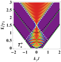
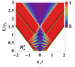
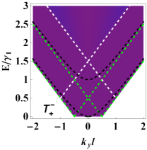
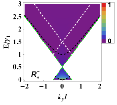
IV.3 AA-2SL-AB
Here we consider the case where the leads consist of BL with different stackings separated by two uncoupled graphene sheets. Such a structure can be formed if in the decoupled region one of the graphene sheets has larger lattice constant, e.g. due to strain, leading to an inter-layer shift when the two layers couple.
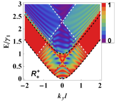
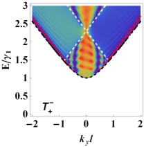
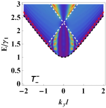
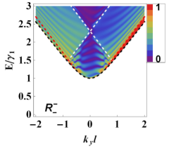
Notice that the inter-layer coupling strength differs for the two bilayer structures. Their ratio is li2009band ; AA-gamma1 ; AA-Yuehua2010 . To account for this difference the energy is normalized to such that the upper Dirac cone of pristine AA-BL is now located at instead of as in the previous sections. In the junction AA-2SL-AB the charge carriers incident from AA-BL and transmitted through 2SL into AB-BL. The results for the transmission and reflection probabilities of this junction are shown in Fig. 24 for and nm. The carriers incident from lower()/upper() Dirac cones in AA-BL can be transmitted into one of the modes ( or ) in the AB-BL, see Fig. 2(e). On the other hand, the reflection process occurs between the intra- or inter-cone in the AA-BL.
Remarkably, Fig. 24 shows that the scattered transmission probabilities are very small and that almost all transmission is carried by the non-scattered channels. This is not immediately expected since a priori the -mode in AA-BL is not related to the -mode in AB-BL. However, both modes have the same parity under in-plane inversion, showing that this feature is robust against variations in the inter-layer coupling.
In contrast to the AA-2SL-AA junction where the scattering between lower and upper cones is forbidden in case of zero bias, here the two cones are coupled even without bias. This results in non-zero reflection in the scattered channels and .
For normal incidence, the scattered transmission ( and ) and the non-scattered reflection ( and ) channels are zero (see Fig. 24) because in that case both the AA and AB Hamiltonian are block diagonal in the even and odd modes basis. Now, we can investigate Klein tunnelling when transitioning in-between the two types of stacking. For this, we show the non-zero channels of transmission and reflection for normal incidence in Fig. 25(a). We find that in contrast with the AA-2SL-AA case, perfect Klein tunnelling does not occur in the junction AA-2SL-AB. However, as shown in Fig. 25(b), we do find that the transmission probability does not depend on the length or even presence of the 2SL region, in contrast to the previous cases with two domain walls.
For the coupling between the different modes is strengthened and, hence, strong scattering in the transmission and reflection channels occurs. Furthermore, the symmetry with respect to normal incidence in the reflection and transmission channels is broken.
The conductance for the discussed structure is shown in Figs. 25(c, d, e) for and (), respectively. For pristine 2SL, the dominant channels are and . Notice that the latter one starts conducting only when and this shows up as a rapid increase in the total conductance at . The scattered channels and are only weakly contributing to the total conductance as a result of weak coupling of the modes. In contrast to the junctions AA(AB)-2SL-AA(AB), in this case the scattered channels of the conductance are not equivalent , see Fig. 25(c,d). This is because the scattering occurs between modes in bilayer graphene of different stackings. The electrostatic potential introduces a minimum at in the total conductance due to the absence of propagating states at this energy in the 2SL, see Fig. 25(d). Biasing the intermediate region (2SL) of the junction AA-2SL-AB provides propagating states at , and hence removing the minima in as shown in Fig. 25(e). In addition, the contribution of the scattered channels and becomes more pronounced as a result of the strong coupling between the modes induced by the bias.
Finally, notice that the counterpart junction AB-2SL-AA, represents the time-reversal case of the system discussed above. We have verified that the transmission channels are equivalent in the absence of a bias. In the presence of a bias, the angular symmetry is broken and, consequently, the reversed junction features the opposite angular asymmetry, preserving time-reversal invariance.
V summary and conclusion
Using the four-band model we obtained the conductance, transmission and reflection probabilities through single and double domain walls separating two single layers and AA/AB-stacked bilayer graphene. We discussed in detail the scattering mechanism from detached layers to bilayer graphene and presented compact analytical formulae for the transmission probabilities. These results showed that one can find the inter-layer coupling strength solely through measuring the conductance.
We found that an electrostatic potential applied to AB-BL, in an 2SL-AB junction, breaks the layer symmetry in the single-valley transmission probability channels. Such asymmetry originates from the asymmetric coupling in AB-BL and arises as a consequence of the mismatch in energy between the 2SL and AB-BL Dirac cones caused by the electrostatic potentials applied to the AB-BL region. Layer asymmetry exists when only one propagating mode is present and hence is not seen in configurations consisting of AA-BL where the entire energy range is associated with two transport channels.
We have also evaluated the robustness of chirality-induced properties, such as Klein tunnelling and anti-Klein tunnelling, to scattering on domains without inter-layer coupling. We found that in domain walls separating 2SL and AA-BL, Klein tunnelling is still preserved. On the other hand, for domain walls separating 2SL and AB-BL, the well known anti-Klein tunnelling in AB-BL is not preserved any more, but neither is Klein tunnelling itself. Moreover, in two domain walls separating three regions whose interlayer coupling is all different, i.e. the AA-2SL-AB case, we find that although perfect Klein tunnelling does not hold, the tunnelling does not depend on the thickness of the 2SL region either. This remarkable effect is attributed to a conservation of parity of the modes.
Furthermore, we have found that a strong gate potential difference allows some states to be localized inside the Mexican hat of the low energy bands in the AB-BL. Those states contribute to the conductance and appear as sharp peaks at the two edges of the gap. We showed that scattering between these modes, in the transmission channels, is not allowed in the configuration (AA/AB)-2SL-(AA/AB). However, such scattering can be induced by applying an inter-layer bias on the 2SL which in addition to shifting the bands of the top and bottom layers of 2SL, also couples the modes. In contrast, we showed that the two modes of AA-BL are coupled even without biasing the system in the junction AA-2SL-AB and revealed that the latter junction is equivalent to the AB-2SL-AA.
In order to limit the number of parameters, through this article we only considered abrupt domain walls, however, the results are robust against smoothness of the domain walls.Hasan1
Our study reveals that the presence of the local domain wall in bilayer graphene samples change the transport properties significantly. Our results may shed light on the design of electronic devices based on bilayer graphene. Finally, we showed that for a given sample with unknown sizes of local stacking domains, the average inter-layer coupling can be estimated through quantum transport measurements.
Acknowledgments
HMA and HB acknowledge the Saudi Center for Theoretical Physics (SCTP) for their generous support and the support of KFUPM under physics research group projects RG1502-1 and RG1502-2. This work is supported by the Flemish Science Foundation (FWO-Vl) by a post-doctoral fellowship (BVD).
Appendix A Functions definitions
The transmission probabilities are calculated by applying appropriate boundary conditions at the 2SL-BL interfaces together with the transfer matrix. After some cumbersome algebra, we obtain for 2SL-AB
| (22) |
where
,
,
,
,
,
.
Similarly, the transmission probabilities for the AB-2SL system are obtained as
| (23) |
with
,
,
and finally
,
where
References
- (1) T. Ohta, A. Bostwick, T. Seyller, K. Horn, and E. Rotenberg, Science 313, 951 (2006).
- (2) E. V. Castro, K. S. Novoselov, S. V. Morozov, N. M. R. Peres, J. M. B. L. dos Santos, J. Nilsson, F. Guinea, A. K. Geim, and A. H. C. Neto, J. Phys.: Condens. Matter 22, 175503 (2010).
- (3) Zhang, Yuanbo, T.-Ta Tang, C. Girit, Z. Hao, M. C. Martin, A. Zettl, M. F. Crommie, Y. R. Shen, and F. Wang, Nature (London) 459, 820 (2009).
- (4) D. R. da Costa, A. Chaves, S. H. R. Sena, G. A. Farias, and F. M. Peeters, Phys. Rev. B 92, 045417 (2015).
- (5) J. W. González, H. Santos, M. Pacheco, L. Chico, and L. Brey, Phys. Rev. B 81, 195406 (2010).
- (6) M. Zarenia, A. Chaves, G. A. Farias, and F. M. Peeters, Phys. Rev. B 84, 245403 (2011).
- (7) I. Silvestre, A. W. Barnard, S. P. Roberts, P. L. McEuen, and R. G. Lacerda, Appl. Phys. Lett. 106 , 153105 (2015).
- (8) X. Zhao, B. Zheng, T. Huang and C. Gao, Nanoscale 7, 9399 (2015).
- (9) S.-H. Ji, J. B. Hannon, R. M. Tromp, V. Perebeinos, J. Tersoff, and F. M. Ross, Nat. Mater. 11, 114 (2012).
- (10) J. M. B. Lopes dos Santos, N. M. R. Peres, and A. H. Castro Neto, Phys. Rev. Lett. 99, 256802 (2007).
- (11) E. J. Mele, Phys. Rev. B 81, 161405(R)(2010).
- (12) J. M. B. Lopes dos Santos, N. M. R. Peres, and A. H. Castro Neto, Phys. Rev. B 86, 155449 (2012).
- (13) A. O. Sboychakov, A. L. Rakhmanov, A. V. Rozhkov, and F. Nori, Phys. Rev. B 92, 075402 (2015).
- (14) M. Van der Donck, F.M. Peeters, and B. Van Duppen, Phys. Rev. B 93, 247401 (2016).
- (15) M. Van der Donck, C. De Beule, B. Partoens, F.M. Peeters, and B. Van Duppen, 2D Mater. 3, 35015 (2016).
- (16) L.-Jing, S. Li, J. Qiao, W. Zuo, and L. He, arXiv:1509.04405 (2015).
- (17) W. Yan, S.Y. Li, L.J. Yin, J. B. Qiao, J.C. Nie, and L. He, Phys. Rev. B 93, 195408 (2016).
- (18) K. W. Clark, X.-G. Zhang, G. Gu, J. Park, G. He, R. M. Feenstra, and A.-P. Li, Phys. Rev. X 4, 011021 (2014).
- (19) M. Pelc, W. Jaskólski, A. Ayuela, and L. Chico, Phys. Rev. B 92, 085433 (2015).
- (20) L. Ju, Z. Shi, N. Nair, Y. Lv, C. Jin, J. Velasco, C. O.-Aristizabal, H.A. Bechtel, M.C. Martin, A. Zettl, J. Analytis, and F. Wang, Nature (London)520, 650 (2015).
- (21) S. Li, H. Jiang, J. Zhou, H. Liu, F. Zhang, and L. He, arXiv:1609.03313 (2016)
- (22) F. Giannazzo, I. Deretzis, A. La Magna, F. Roccaforte, and R. Yakimova, Phys. Rev. B 86, 235422 (2012).
- (23) A. Nourbakhsh, M. Cantoro, A. V. Klekachev, G. Pourtois, T. Vosch, J. Hofkens, M. H. van der Veen, M. M. Heyns, S. De Gendt, and B. F. Sels, J. Phys. Chem. C 115, 16619 (2011).
- (24) B. Z. Rameshti, M. Zareyan, and A. G. Moghaddam, Phys. Rev. B 92, 085403 (2015).
- (25) T. Nakanishi, M. Koshino, and T. Ando, J. Phys.: Conf. Ser. 302, 012021 (2011).
- (26) T. Nakanishi, M. Koshino, and T. Ando, Phys. Rev. B 82, 125428 (2010).
- (27) J. Nilsson, A. H. Castro Neto, F. Guinea, and N. M. R. Peres, Phys. Rev. B 76, 165416 (2007).
- (28) C. P. Puls, N. E. Staley, and Y. Liu, Phys. Rev. B 79, 235415 (2009).
- (29) M. Koshino, T. Nakanishi, and T. Ando, Phys. Rev. B 82, 205436 (2010).
- (30) J. Tian, Y. Jiang, I. Childres, H. Cao, J. Hu, and Y. P. Chen, Phys. Rev. B 88, 125410 (2013).
- (31) D. Yin, W. Liu, X. Li, L. Geng, X.Wang, and P. Huai, Appl. Phys. Lett. 103, 173519 (2013).
- (32) M. Berahman, M. Sanaee, and R. Ghayour, Carbon 75, 411 (2014).
- (33) D. Dragoman, J. Appl. Phys. 113, 214312 (2013).
- (34) Y. Hasegawa and M. Kohmoto, Phys. Rev. B 85, 125430 (2012).
- (35) H. Li, H. Li, Y. Zheng, and J. Niu, Physica B 406, 1385 (2011).
- (36) Z. X. Hu and W. Ding, Phys. Lett. A 376, 610 (2012).
- (37) Y. Wang, J. Appl. Phys. 116, 164317 (2014).
- (38) J. W. González, H. Santos, E. Prada, L. Brey, and L. Chico, Phys. Rev. B 83, 205402 (2011).
- (39) B. Wang, M. Huang, N. Y. Kim, B. V. Cunning, Y. Huang, D. Qu, X. Chen, S. Jin, M. Biswal, X. Zhang, S. H. Lee, H. Lim, W. J. Yoo, Z. Lee, and R. S. Ruoff, Nano Lett. 17, 1467 (2017).
- (40) J. C. Rode, C. Belke, H. Schmidt, and R. J. Haug, arXiv: 1608.08133v1 (2016).
- (41) M. Schmitz, S. Engels, L. Banszerus, K. Watanabe, T. Taniguchi, C. Stampfer, and B. Beschoten, p. arXiv:1704.04352 (2017).
- (42) W. Yan, S.-Y. Li, L.-J. Yin, J.-B. Qiao, J.-C. Nie, and L. He, Phys. Rev. B 93, 195408 (2016).
- (43) Y. Hao, L. Wang, Y. Liu, H. Chen, X. Wang, C. Tan, S. Nie, J. W. Suk, T. Jiang, T. Liang, J. Xiao, W. Ye, C. R. Dean, B. I. Yakobson, K. F. McCarty, P. Kim, J. Hone, L. Colombo, and R. S. Ruoff, Nat. Nanotechnol. 11, 426 (2016).
- (44) L.-J. Yin, W.-X. Wang, Y. Zhang, Y.-Y. Ou, H.-T. Zhang, C.-Y. Shen, and L. He, Phys. Rev. B 95, 081402(R) (2017).
- (45) L.-J. Yin, H. Jiang, J.-B. Qiao, and L. He, Nat. Commun. 7, 11760 (2016).
- (46) M. I. Katsnelson, K. S. Novoselov, and A. K. Geim, Nat. Phys. 2, 620 (2006).
- (47) N. Stander, B. Huard, and D. Goldhaber-Gordon, Phys. Rev. Lett. 102, 026807 (2009).
- (48) A. H. C. Neto, F. Guinea, N. M. R. Peres, K. S. Novoselov, and A. K. Geim, Rev. Mod. Phys. 81, 109 (2009).
- (49) Z. Q. Li, E. A. Henriksen, Z. Jiang, Z. Hao, M. C. Martin, P. Kim, H. L. Stormer, and D. N. Basov, Phys. Rev. Lett. 102, 037403 (2009).
- (50) B. Van Duppen and F. M. Peeters, Phys. Rev. B 87, 205427 (2013).
- (51) I. Lobato and B. Partoens, Phys. Rev. B 83, 165429 (2011).
- (52) Y. Xu, X. Li, L. Reining, and J. Dong, Nanotechnology 21, 065711 (2010).
- (53) M. Sanderson, Y. S. Ang, and C. Zhang, Phys. Rev. B 88, 245404 (2013).
- (54) M. Barbier, P. Vasilopoulos, and F. M. Peeters, Phys. Rev. B. 82, 235408 (2010).
- (55) B. Van Duppen, S. H. R. Sena, and F. M. Peeters, Phys. Rev. B 87, 195439 (2013).
- (56) Ya. M. Blanter and M. Buttiker, Phys. Rep. 336, 1 (2000).
- (57) S. B. Kumar and J. Guo, Appl. Phys. Lett. 100, 163102 (2012).
- (58) B. Van Duppen and F. M. Peeters, Appl. Phys. Lett. 101, 226101 (2012).
- (59) H. M. Abdullah, M. Zarenia, H. Bahlouli, F. M. Peeters and B. Van Duppen, EPL 113, 1 (2016).
- (60) I. Snyman and C. W. J. Beenakker, Phys. Rev. B 75, 045322 (2007).
- (61) D. R. da Costa, A. Chaves, S. H. R. Sena, G. A. Farias, and F. M. Peeters, Phys. Rev. B 92, 045417 (2015).
- (62) A. Rycerz, J. Tworzydło, and C. W. J. Beenakker, Nat. Phys. 3, 172 (2007).
- (63) L. R. F. Lima, A. R. Hernández, F. A. Pinheiro and C. Lewenkopf, J. Phys.: Condens. Matter 28, 505303 (2016).
- (64) P. Brandimarte, M. Engelund, N. Papior, A. Garcia-Lekue, T. Frederiksen, and D. Sánchez-Portal, arXiv:1611.03337(2016).
- (65) M. R. Masir, P. Vasilopoulos, and F. M. Peeters, Physical Review B 82, 115417 (2010).