Design, Fabrication, and Characterization of Ta2O5 Photonic Strip Waveguides
Abstract
Efficient coupling of single quantum emitters to guided optical modes of integrated optical devices is of high importance for applications in quantum information science as well as in the field of sensing. Here we present the design and fabrication of a platform for on-chip experiments based on dielectric optical single-mode waveguides (Ta2O5 on SiO2). The design of the waveguide is optimized for broadband (600-800 nm) evanescent coupling to a single quantum emitter (expected efficiency: up to 36%) and efficient off-chip coupling to single-mode optical fibers using inverted tapers. First test samples exhibit propagation losses below 1.8 dB/mm and off-chip coupling efficiencies exceeding 57%. These results are promising for efficient coupling of solid state quantum emitters like NV- and SiV-centers to a single optical mode of a nano-scale waveguide.
pacs:
03.67.-a, 07.79.-v, 42.50.Ex, 78.67.BfIntroduction: On-chip evanescent coupling of light radiated by a single quantum emitter to a waveguide mode has a great potential in the field of integrated quantum information science [1, 2]. Such devices provide e.g. an attractive platform for applications where projective on-chip measurements on photon-pairs mediate entanglement between widely separated quantum emitters [3, 4]. In this context, the most basic device is a single photon emitter efficiently coupled to a single optical mode [5, 6, 7] which then guides the photons with low loss to a detector.
The requirements on such a photonic platform can be separated into three parts. First, the quantum system (or quantum emitter) has to be optically coupled to a waveguide. Second, the waveguide is expected to transport the photons in a confined mode with low loss. Third, the system is required to be able to couple the photons to another quantum system, device, or the macroscopic world (i.e. for instance an external photo detector). These three aspects pose different, partly even contradictory requirements on the experimental realization. Here we present the design, fabrication, and characterization of a planar single mode waveguide addressing all three aspects by featuring broadband efficient evanescent coupling to fluorescent quantum emitters combined with low-loss guidance and efficient off-chip coupling to single mode optical fibers.
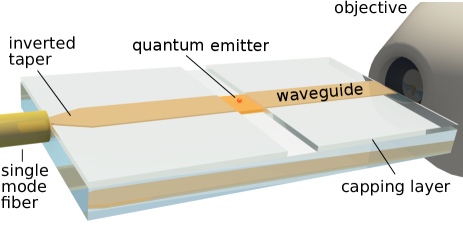
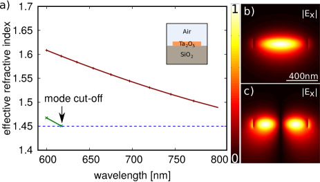
Design: Our nanoscale waveguide (see Fig. 1) is designed to provide a versatile platform for on-chip optics allowing at the same time efficient evanescent optical coupling to various kind of solid state quantum emitters like colloidal quantum dots or defect centers in nanodiamonds. For the waveguide core we have chosen the high refractive index dielectric Ta2O5 [8], whereas the lower cladding material is fused silica. Both materials show a low autofluorescence [9], an important property for sensitive experiments at the single emitter level. In order to enable efficient channeling of emitter fluorescence to the waveguide, the vacuum electric field of the guided mode at the position of the emitter has to be maximized [10]. Therefore, in a first step the evanescent electric field (at the waveguide-air interface) was maximized by minimizing the height of the planar waveguide, yielding an optimal value of 100 nm. In a second step the width of the waveguide was optimized to 700 nm with the help of a vectorial mode solver (Mode Solutions from Lumerical) to provide single mode operation for wavelengths from 620 nm to 800 nm (see Fig. 2). Here we emphasize that due to the broken top-bottom symmetry of the refractive indexes of the cladding (see inset of Fig. 2(a)) the height can not be reduced below a critical value of 90 nm to assure confinement of the fundamental mode in the high-refractive core.
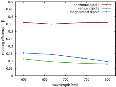
After we have fixed the waveguide geometry, we additionally performed numerical FDTD simulations to estimate the expected radiative coupling efficiency of a quantum emitter to the fundamental eigenmode (see Fig. 2(b)). We modeled the quantum emitter as a linear dipole positioned at the air-core interface. Similar to analytical calculations with a dipole coupled to the nanofiber-section of a tapered optical fiber [11] we find broadband coupling efficiencies (quantified by the spontaneous emission coupling parameter ) [10] for all three dipole polarizations (horizontal, vertical, longitudinal) yielding typical values around (0.35, 0.1, 0.15), respectively (see Fig. 3).
In order to transport the guided photons to other experimental devices which are not integrated on the chip itself off-chip-coupling to standard single mode fibers is helpful. We use an inverted in-plane tapering of the asymmetric waveguide [12] to adiabatically transform the waveguide mode such that the overlap with the mode of a standard single mode fiber is maximized.
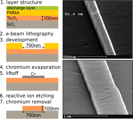
Fabrication: The waveguides and inverted tapers are fabricated using two major key technologies, i.e. electron beam lithography (EBL) and reactive ion etching (RIE). In more detail, nano-fabrication of the waveguide structures proceeds as follows.
The sample wafer consists of a synthetic fused silica substrate coated with a 100 nm thick layer of Ta2O5 in a sputtering process (by asphericon GmbH, Jena, Germany). For electron beam lithography (EBL) the sample is first spin-coated (1s at 800 rpm and 30s at 5000 rpm) with PMMA (950k A4 from Microchem) as EBL-resist and then soft-baked on a hotplate for 15 min at 170∘C. This results in a PMMA-layer thickness of about 190 nm. Then, the sample is spin-coated (30 s at 2000 rpm) with a conductive polymer (SX AR-PC 5000/90.1, Allresist GmbH), which acts as discharge layer during the electron beam exposure. Compared to a standard metal discharge layer (like chromium) a conductive polymer promises improved roughness [13] of the waveguide side-walls.
The EBL of the waveguides and inverted tapers is performed with a Raith e_LiNE with an applied acceleration voltage of 10 kV. The shape of the waveguides is written with a moving sample stage and a spatially fixed electron beam while the inverted taper is written in the standard vector scanning mode using an optimal dose of 95 C/cm2. Immediately after EBL exposure the conductive polymer is removed with clean nitrogen gas and deionized water (LicoJET mini high pressure cleaner, Lico-Tec GmbH). The e-beam resist is developed in 3:1 IPA:MIBK and 1.5% MEK at room temperature for 50 s followed by a short cleaning-step in IPA. Now, the sample is coated with the hard mask material (8 nm of chromium) using an electron beam evaporator in a high vacuum coating plant. The liftoff is mediated by preheated DMSO at 90∘ C for more than 2 hours. Finally the sample is rinsed with acetone and IPA to remove any residual contaminants. The hard mask pattern is transfered to the Ta2O5 with inductively coupled plasma reactive ion etching (ICP-RIE) in an Oxford Instruments Plasmalab System 100. As processing gas SF6 is used diluted with Ar (4:1 in volume) with a pressure of 5 mtorr. The ICP-power was optimized to 70 W with a RF-power of 100 W. With these parameters the 100 nm layer of Ta2O5 is removed completely within 1:40 min. Now, the mask is removed with a liquid chromium etchant.
For butt-coupling the end facet quality of the waveguides is crucial. Therefore a layer of 3 m of SiO2 is sputtered on top of the waveguides. In order to retain an area where the waveguides are sensitive to emitters this part is masked during the sputtering process. The end facets were finished with a Ultratec Minipol polisher and polishing pads provided by Ultrapol for standard FC/PC fibers. After processing a few seconds per pad no scratches and inhomogeneities were visible in an optical inspection microscope.
Characterization: For optical characterization, the measured transmission of the fabricated waveguides is compared for different waveguide lengths (cut-back method). On the logarithmic scale the total transmission loss introduced by the waveguide is given by the sum of the in-coupling loss , the propagation loss times propagation distance , and the out-coupling loss
A linear fit of the measured total transmission loss for different waveguide lengths allows than to determine the propagation and insertion loss.
The cut-back measurement is performed with a waveguide sample with an inverted taper on one side only. The sample is shortened from the side without taper to keep the in- and out-coupling mode geometries constant. In order to determine the transmission, probe laser light (wavelength: 658 nm) guided by a polarization compensated single mode fiber is coupled via butt-coupling into the waveguide (see illustration in Fig. 1). The light emerging from the output of the waveguide is collected with a microscope objective and imaged onto a CCD camera or a calibrated photo-diode. Here, without inverted taper, the high mode confinement results in a high divergence of the output mode. Within the numerical aperture of the objective (NA=0.65) 62.3% of this mode can be collected (obtained from simulations of the mode-profile). This value is the minimum achievable out-coupling loss in our experiment and is fixed for all measurements. The unprocessed transmission data is plotted against the waveguide length in Fig. 5. From this data a propagation loss below 1.8 dB/mm as well as insertion loss below 2.4 dB (57% transmission) were obtained for at least two of the 4 inspected waveguides of the chip (see Tab. 1). To avoid additional scattering losses during the cut-back measurements the sample was fully covered by a SiO2 capping layer.
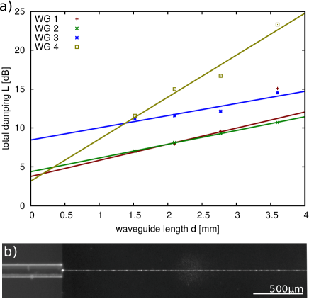
| Waveguide | Prop. loss | Insertion loss |
|---|---|---|
| 1 | (2.070.24) dB/mm | (1.690.53) dB |
| 2 | (1.770.03) dB/mm | (2.310.08) dB |
| 3 | (1.560.40) dB/mm | (6.391.05) dB |
| 4 | (5.400.76) dB/mm | (1.091.99) dB |
Discussion: A dielectric on-chip waveguide has been designed to provide a versatile platform for on-chip experiments in quantum information science and sensing applications. The waveguide promises moderate coupling efficiencies of about 35% to a dipole placed on its surface and aligned parallel to the long axis of the waveguide. To realize first samples, a fabrication process has been developed based on nano-fabrication techniques such as electron beam lithography and reactive ion etching. The electron beam lithography process allows to pattern continuous waveguides of several millimeters in length which can be connected to arbitrary structures without stitching errors. The overall process was optimized to get reproducible propagation losses below dB/mm at an operation wavelength of 658 nm. This experimental finding is in good agreement with an estimated value of dB/mm on basis of the Payne-Lacey model, which uses the measured sidewall-roughness (determined via independent AFM investigations [14]) as input parameter. In the literature propagation losses as low as dB/cm have been reported [15] using the same material system (Ta2O5 on SiO2), but with much bigger dimensions (200 nm x 2…10 m) and light with a longer wavelength (1070 nm). However, with a system more comparable in geometry, Fu et al. [16] found propagation loss of 4.63 dB/mm for a rig waveguide of 1 m in width and 160 nm in hight (GaP on diamond).
To provide efficient off-chip coupling to standard single-mode fibers an inverted taper was added to the waveguide. For our fabricated samples we find typical off-chip coupling efficiencies of 57%. With the values achieved for propagation length and off-chip coupling, combined with the expected coupling-efficiency from the emitter to the waveguide, a total coupling from the emitter to a standard fiber-coupled APD-detector of above 10% is realistic. Further progress in fabrication can then pave the way to slot waveguides [10], cavities with distributed Bragg reflectors, or even a combination of both [17] promising emitter to waveguide coupling of up to 65% [18].
Acknowledgments
We acknowledge funding from the DFG through the excellence cluster NIM and the Forschergruppe 1493. TT acknowledges support from the Japanese Society for the Promotion of Science.
References
References
- [1] E. Knill, R. Laflamme, and G. J. Milburn, Nature 409, 46 (2001).
- [2] J. E. Kennard, J. P. Hadden, L. Marseglia, I. Aharonovich, S. Castelletto, B. R. Patton, A. Politi, J. C. F. Matthews, A. G. Sinclair, B. C. Gibson, S. Prawer, J. G. Rarity, and J. L. O’Brien, Phys. Rev. Lett. 111, 213603 (2013).
- [3] Jürgen Volz, Markus Weber et al., Phys. Rev. Lett. 96, 030404 (2006).
- [4] J. Hofmann, M. Krug, N. Ortegel, L. Gerard, M. Weber, W. Rosenfeld, H. Weinfurter, Science 337, 72 (2012).
- [5] Dirk Englund, Brendan Shields, Kelley Rivoire, Fariba Hatami, Jelena Vučković, Hongkun Park, and Mikhail D. Lukin , Nano Lett. 10, 3922 (2010).
- [6] Andrei Faraon, Charles Santori, Zhihong Huang, Victor M. Acosta, and Raymond G. Beausoleil, Phys. Rev. Lett. 109, 033604 (2012).
- [7] L. Liebermeister, F. Petersen, A. Muünchow, D. Burchardt, J. Hermelbracht, T. Tashima, A. Schell, O. Benson, T. Meinhardt, A. Krueger, A. Stiebeiner, A. Rauschenbeutel, H. Weinfurter, and M. Weber, Appl. Phys. Lett. 104, 031101 (2014).
- [8] Uwe Huebner, R. Boucher, W. Morgenroth, J. Kunert, H. Roth, H.-G. Meyer, T. Glaser, S. Schroeter, Microelectronic Engineering 78–79, 422 (2005).
- [9] Y. Zhao, M. Jenkins, P. Measor, K. Leake, S. Liu, H. Schmidt and A. R. Hawkins, Appl. Phys. Lett. 98, 091104 (2011).
- [10] Qimin Quan, Irfan Bulu, and Marko Lončar, Phys. Rev. A 80, 011810(R) (2009).
- [11] F. L. Kien, J. Q. Liang, K. Hakuta, and V. I. Balykin, Opt. Commun. 242, 445 (2004).
- [12] Vilson R. Almeida, Roberto R. Panepucci, and Michal Lipson, Optics Letters 28, 1302 (2003).
- [13] Mustafa Muhammad, Steven C. Buswell, Steven K. Dew and Maria Stepanova, J. Vac. Sci. Technol. B 29, 06F304 (2011).
- [14] Niko Heinrichs, master thesis, LMU Munich 2015.
- [15] Ahluwalia, B. S., Hellesø, O. G., Subramanian, A. Z., Perney, N. M., Sessions, N. P., and Wilkinson, J. S., SPIE proceedings 7604, 76040W (2010).
- [16] K.-M. C. Fu, C. Santori, P. E. Barclay, I. Aharonovich, S. Prawer, N. Meyer, A. M. Holm and R. G. Beausoleil, Appl. Phys. Lett. 93, 234107 (2008).
- [17] Xu Wang, Samantha Grist, Jonas Flueckiger, Nicolas A. F. Jaeger, and Lukas Chrostowski; Optics Express 21, 19029 (2013).
- [18] Peter Fischer, master thesis, LMU Munich 2015.