11email: hlm2124@columbia.edu 22institutetext: School of Physics and Astronomy, Cardiff University, Cardiff, Wales CF24 3AA, UK 33institutetext: School of Earth and Space Exploration, Arizona State University, Tempe, AZ 85287, USA 44institutetext: Jet Propulsion Laboratory, Pasadena, CA 91109, USA 55institutetext: Goddard Space Flight Center, Greenbelt, MD 20771, USA 66institutetext: Department of Physics and Astronomy, University of Southern California, Los Angeles, CA 90089, USA
Design and performance of dual-polarization lumped-element kinetic inductance detectors for millimeter-wave polarimetry
Abstract
Aims. Lumped-element kinetic inductance detectors (LEKIDs) are an attractive technology for millimeter-wave observations that require large arrays of extremely low-noise detectors. We designed, fabricated and characterized 64-element (128 LEKID) arrays of horn-coupled, dual-polarization LEKIDs optimized for ground-based CMB polarimetry. Our devices are sensitive to two orthogonal polarizations in a single spectral band centered on 150 GHz with . The mm square arrays are designed to be tiled into the focal plane of an optical system. We demonstrate the viability of these dual-polarization LEKIDs with laboratory measurements.
Methods. The LEKID modules are tested with an FPGA-based readout system in a sub-kelvin cryostat that uses a two-stage adiabatic demagnetization refrigerator. The devices are characterized using a blackbody and a millimeter-wave source. The polarization properties are measured with a cryogenic stepped half-wave plate. We measure the resonator parameters and the detector sensitivity, noise spectrum, dynamic range, and polarization response.
Results. The resonators have internal quality factors approaching . The detectors have uniform response between orthogonal polarizations and a large dynamic range. The detectors are photon-noise limited above 1 pW of absorbed power. The noise-equivalent temperatures under a 3.4 K blackbody load are . The polarization fractions of detectors sensitive to orthogonal polarizations are . The entire array is multiplexed on a single readout line, demonstrating a multiplexing factor of 128. The array and readout meet the requirements for 4 arrays to be read out simultaneously for a multiplexing factor of 512.
Conclusions. This laboratory study demonstrates the first dual-polarization LEKID array optimized specifically for CMB polarimetry and shows the readiness of the detectors for on-sky observations.
Key Words.:
Instrumentation: detectors – Instrumentation: polarimeters – cosmic background radiation1 Introduction
Lumped-element kinetic inductance detectors (LEKIDs) are planar, superconducting LC resonators that are also photon absorbers. An absorbed photon with an energy greater than , where is the superconducting gap, will break Cooper pair(s) increasing the quasiparticle density , dissipation, and kinetic inductance (Day et al., 2003; Doyle et al., 2008). This results in a shift in the resonator quality factor and resonance frequency , which is read out by monitoring a probe tone that is driving the device at its nominal resonance frequency. Each LEKID has a unique resonance frequency set by the geometry of the capacitor. This architecture naturally allows for frequency multiplexing because an array of LEKIDs can be read out on a single transmission line.
Kinetic inductance detectors (KIDs) have been developed for a wide range of wavelengths (Calvo et al., 2016; McCarrick et al., 2014; Mazin et al., 2013; Swenson et al., 2012). Significant advances have been made in developing dual-polarization and multi-chroic KIDS (Dober et al., 2016; McCarrick et al., 2016; Johnson et al., 2016), demonstrating photon-noise dominated sensitivity (Bueno et al., 2016; Flanigan et al., 2016; Hubmayr et al., 2015; Mauskopf et al., 2014; Janssen et al., 2013), determining space-readiness in the far infrared (FIR) (Baselmans et al., 2017), and deploying arrays for astrophysical observations (Adam et al., 2017, 2014; Szypryt et al., 2014).
In this paper we describe the design and measured performance of dual-polarization LEKIDs optimized for cosmic microwave background (CMB) studies. CMB experiments are being designed to search for the divergence-free component of the polarization signal, often referred to as the B-mode signal, which would provide strong evidence for inflation after the Big Bang (Knox & Song, 2002; Seljak & Zaldarriaga, 1997; Kamionkowski et al., 1997). The anticipated primordial B-mode signal is faint when compared with the unavoidable photon noise in the CMB itself, and current instruments already use photon-noise limited detectors (Stebor et al., 2016; Henderson et al., 2016; Posada et al., 2016; Harrington et al., 2016; Grayson et al., 2016). Therefore, to increase instrument sensitivity going forward, the number of detectors must be increased, so scalable detector technologies with high multiplexing factors are needed for next-generation CMB experiments (Abitbol et al., 2017). LEKIDs could be an attractive option for these next-generation experiments, so we conducted the laboratory study described in this paper to investigate their suitability. In particular, we focused on measuring the sensitivity and polarization selectivity of our design to see if it is viable, and we tested a multiplexing factor of 128 that advances the state-of-the-art for CMB experiments.
The paper is organized as follows: In Section 2.1, we present the detector requirements and subsequent design. In Section 2.2, we discuss the optical coupling and array design. In Section 2.3, we describe the experimental system. In Section 3, we present the tests undertaken to characterize the detectors including measurements of the resonator parameters, optical response, dynamic range, noise, and polarization selectivity. In Section 4, we discuss the measurement results.
2 Methods
2.1 Detector requirements and design
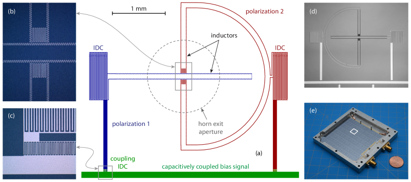
The dual-polarization LEKIDs are laid out in an square array with a 7.8 mm pitch (see Fig. 1e). Each array element consists of two resonators for a total of 128 LEKIDs per array. The array element design is shown in Fig. 1. The two resonators are sensitive to orthogonal polarizations for observation in a single spectral band centered on 150 GHz. Each resonator consists of an inductor connected in parallel with an interdigitated capacitor (IDC). The inductors for each pixel are identical across the array. Each IDC has a unique capacitance and thus each resonator has a unique . Therefore the detectors naturally lend themselves to frequency multiplexing.
The arrays are fabricated on high-resistivity (¿ 10 kcm) silicon wafers. After the detector processing steps are completed, the silicon is thinned to 160 m by grinding the back side of the wafer. As the final step, the arrays are diced into squares, which are designed to be tiled. The total number of detectors in each array is therefore determined by the choice of pitch and the decision to use 100 mm diameter wafers as the substrate.
The resonators are capacitively coupled to a 50 microstrip transmission line. We chose to metalize the back side of the wafer with a 100 nm thick aluminum (Al) film to provide a ground plane for both the microstrip and the resonators and to optimize the millimeter-wave coupling (see Fig. 2 and Sec. 2.2). The detectors and transmission line are made out of a single Al film that is 25 nm thick. Wirebonds connect the Al microstrip to the rest of the readout chain (see Sec. 2.3.2). We measured the critical temperature of the film to be 1.4 K.
The absorbing element of the detector is the inductor. In our design, the geometry of one inductor is a single, long trace in the shape of a hairpin, while the orthogonal inductor is composed of two hairpins. We chose this architecture so the array can be fabricated with a single film without crossovers.
The detectors are designed for ground-based CMB experiments which have an expected loading of 1 to 10 pW. We started with straight inductors (Bryan et al., 2015; McCarrick et al., 2016) but found for this absorber geometry the resonator quality factor degraded too rapidly as a function of absorbed power . To retain sufficiently high under ground based loading conditions, we increased the volume of the inductor. Solely increasing the film thickness would decrease the surface impedance of the absorber, causing poor coupling to the incoming radiation. Therefore, was tuned by ‘wiggling’ the trace in alternating semi-circles as shown in the photograph in Fig. 1b. Wiggling the inductors allows us to add more volume by increasing both the length and film thickness while maintaining a similar effective surface impedance to the millimeter-wave radiation. The wiggles increase the length of the inductors as compared with a straight meander by a factor of /2. To maintain the surface impedance needed for high optical coupling, we made the film thickness 25 nm. The detector response is defined as the ratio of the change in the fractional frequency shift
| (1) |
to the change in absorbed power. As a result of the increased volume, we expect to decrease as compared with the straight inductor for a given .
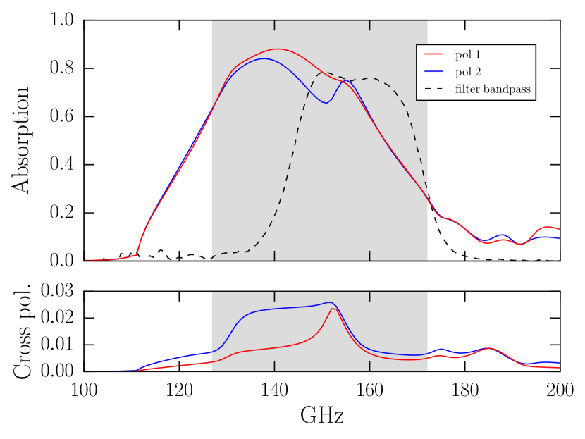
The inductors are naturally polarization sensitive, preferentially absorbing radiation with the E-field aligned to the inductor trace. Electromagnetic simulations111ANSYS Electronics Desktop 2016 were used to optimize the design so that the two polarizations have similar absorption spectra. The simulations included the detector and array design starting from the waveguide (see Sec. 2.2) through the array backshort (see Fig. 2). We found it necessary to meander the end of the polarization-1 inductor (see Fig. 1) to minimize absorption of the cross-polarization. The simulated absorption spectra and cross-polarization spectra are shown in Fig. 3.
We have designed arrays with resonance frequencies in the 100–200 MHz or 800–1200 MHz bands. The arrays are fabricated with a stepper. Each stepper field contains a sub-array of dual-polarization LEKIDs, so an array is comprised of 16 stepper fields. The stepper fields are exposed in a array across the wafer to make the full array of dual-polarization LEKIDs. Each stepper field is exposed in two steps. First, the fixed portion of the design, including the inductors, coupling capacitors, transmission line segments, and half of each IDC structure, is exposed identically for each stepper field. A second stepper field including the second half of the IDC structures is then exposed with a relative offset that varies across the wafer. The capacitor lengths set by this relative offset increase linearly across the wafer, resulting in a weakly quadratic frequency spacing across the readout bandwidth. Within each stepper field, the resonance frequencies of the detectors are spaced maximally far apart over the array readout bandwidth to decrease the likelihood of adjacent resonators coupling to one another in frequency space (Noroozian et al., 2012). The resonance frequencies for the two polarizations are separated into a high and low band within the readout bandwidth of the array.
Our LEKID readout system provides a bandwidth of 250 MHz at baseband frequencies (0–250 MHz) or 500 MHz when using an IQ mixer to target readout frequencies in the range 0.5–4.0 GHz. Although we are demonstrating a multiplexing factor of 128 here, our design goal is to read out 4 modules with a single readout system so we are designing for a future multiplexing factor of 512. To avoid collisions between detectors, we choose a resonance frequency spacing of 10 times the resonance width. This choice means the of the resonators needs to be . The resonator quality factor is determined as
| (2) |
where is the internal quality factor and is the coupling quality factor. We chose to be approximately which is set by the value of the coupling capacitor (see Fig. 1). These fabricated devices have under an optical load, which is higher than we expected, so the coupling quality factor predominately sets the total as . Ideally, under the desired optical load (Zmuidzinas, 2012), so in future iterations of the design the coupling capacitance will be decreased.
2.2 Detector array design
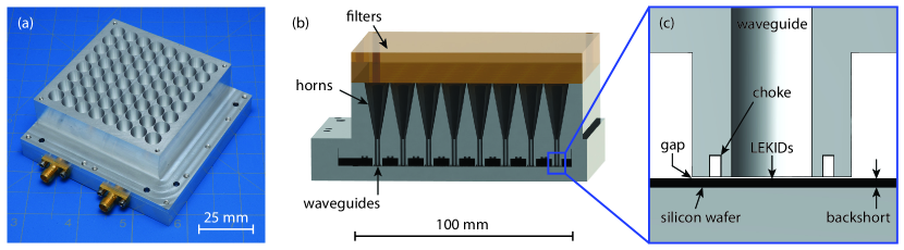
The absorption band is defined by metal mesh filters mounted in front of the horn apertures. The bandwidth is defined by a band-pass filter with a measured spectrum from 140–170 GHz as plotted in Fig. 3. For future tests or observations, it would be advantageous to use a wider bandpass filter which more closely matches the absorption spectra of the detectors. Additional low-pass and high-pass filters suppress out-of-band spectral leaks.
The detectors are fed with conicals horns that have a 7.8 mm aperture and a flare angle (see Fig. 2). One horn feeds one array element (two LEKIDs) so the horns are arranged an square array with a 7.8 mm pitch. The horns are designed to couple to an F/2.5 optical system, which means the aperture diameter is 1.6 F at 150 GHz.
The horn flare feeds a cylindrical waveguide with a 1.6 mm diameter. This waveguide diameter has a cut-on frequency below the low-frequency edge of the spectral band defined by the band-pass filter. We chose this diameter because it works well with a profiled-horn design we are developing. Future LEKID modules will use these profiled horns because simulations show the horn beam is more circular. A choke at the waveguide output optimizes detector coupling and minimizes the lateral leakage of fields that can produce crosstalk between detectors. A vacuum gap of 30 m then precedes the LEKIDs. The 160 m wafer thickness sets the backshort distance. The metalized ground plane on the backside of the wafer also acts as the backshort, increasing the absorption efficiency of each LEKID.
The LEKID array is mounted to the bottom part of a two-part aluminum package, the top of which is the horn array. The detector array is edge aligned against dowel pins mounted in the bottom of the package. The same pins are used to co-align the horn array in the package lid with the LEKID array in the package bottom. The array is held in place by three beryllium-copper clips positioned in corners of the LEKID array. Small spring-loaded pins222Mill-Max Manufacturing Corp. ED9000-ND epoxied3333M Scotch-Weld Epoxy Adhesive DP420 Black into the package lid press down on the LEKID array in ten positions when the module is assembled. These spring-loaded pins help suppress vibrations in the array, which can produce features in the noise spectra (see Sec. 3.3). To improve the heat sinking of the silicon substrate, gold bars were patterned on the edge of the detector array and wirebonds connect these bars to the package bottom.
2.3 Experimental system
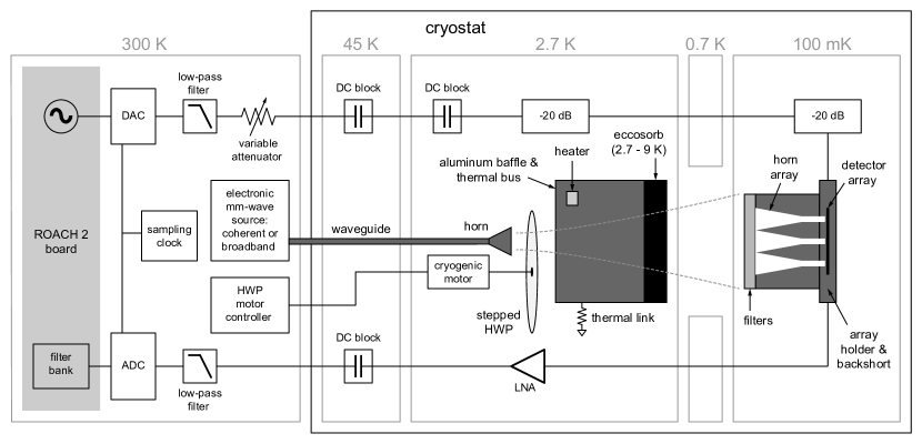
2.3.1 Cryogenics
The experimental system is schematically depicted in Fig. 4. The detectors are mounted inside a cryostat444DRC-102 Cryostat System made by STAR Cryoelectronics that uses a two-stage adiabatic demagnetization refrigerator (ADR) backed by a two-stage pulse tube cooler (PTC). The PTC provides 45 K and 2.7 K temperature stages, while the ADR provides a 0.7 K stage and a variable 60–300 mK stage. The detectors are mounted on the variable, sub-kelvin stage.
2.3.2 Readout
The readout system used for this study is based on the open-source ROACH-2 board, which hosts a Xilinx Virtex-6 FPGA. The ROACH-2 board555Digicom Electronics is combined with an ADC/DAC daughter board666Techne Instruments that provides two 12-bit ADCs and two 16-bit DACs, each capable of synthesizing and analyzing signals with 250 MHz of bandwidth.
We have designed two varieties of LEKID arrays. For one variety, the frequencies are designed to be in the range 100–200 MHz and the other in the range 800–1200 MHz. The signals used to read out the lower-frequency 100–200 MHz resonators can be directly synthesized and analyzed using the ADC/DAC board. In this case, the only additional analog signal conditioning hardware needed is a variable attenuator and a warm amplifier. For the higher frequency 800–1200 MHz readout band, quadrature mixers are added to up and down-convert the baseband signals (Johnson et al., 2016).
The LEKID readout system uses a heterogeneous architecture, where the real-time signal processing is split between the ROACH-2 board and the readout computer attached to it. This architecture provides flexibility, allowing us to save time series at full bandwidth (10 kHz) for diagnostic purposes, as well as low pass filtered signals appropriate for the bandwidth of signals expected while observing with a continuously rotating half-wave plate (HWP) (200 Hz) in a deployed instrument.
2.3.3 Millimeter-wave sources
The system to optically characterize the LEKIDs consists of three main components: (i) a variable blackbody source, (ii) an electronic millimeter-wave (MMW) source that can produce broadband or coherent radiation, and (iii) a stepped HWP. A diagram of the optical layout is shown in Fig. 4.
The blackbody load is a beam-filling piece of Eccosorb absorber (13 mm thick), which is anti-reflection (AR) coated with etched Teflon (380 m thick). It is weakly thermally coupled to the 2.7 K stage. The blackbody temperature can be adjusted from 3–9 K using a resistive heater.
The MMW source is mounted outside the cryostat. A WR6 directional coupler splits the source signal. Radiation from one port is routed into the cryostat via WR6 waveguide and then launched from a conical horn through the HWP. Radiation from the second port is used to continuously measure the power emitted by the source using a calibrated zero-bias detector (ZBD). The MMW source can be operated in broadband mode (140–165 GHz) or continuous wave mode (Flanigan et al., 2016). In continuous wave mode, the frequency of the single tone can be swept.
The polarization orientation of the source signals can be rotated with the stepped HWP. The HWP is sapphire (3.2 mm thick) with fused silica AR coatings (0.28 mm thick). The HWP is rotated by a cryogenic motor mounted at 2.7 K controlled by an Arduino-based system at room temperature. After the HWP, Eccosorb, which is mounted on an aluminum thermal bus, acts as an 11 dB attenuator for the millimeter-radiation. The Eccosorb therefore acts both as the blackbody source and as an attenuator in the path of the radiation from the MMW source. The capabilities of this system allow us to measure the detector noise spectra, responsivity, absorption spectra, and polarization selectivity.
3 Results
The experiments described in the following section refer to a single 128 resonator array with resonance frequencies that fall between 110–170 MHz. We performed a sequence of cryogenic cooldowns in the following configurations: (i) the horn array was removed and an aluminum plate closed the package, (ii) all horn apertures were illuminated by the sources, and (iii) all but one horn aperture was covered.
3.1 Resonator characterization
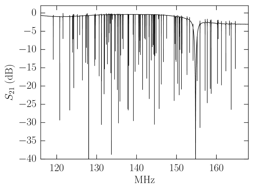
For the first test, the detectors were enclosed in a sealed box and not illuminated by any of the aforementioned sources. The temperature of the array was held at 120 mK. We measured , the forward scattering parameter, across the array, as shown in Fig. 5 and identified the resonance frequencies. This measurement revealed 100 out of 128 resonators for a 78% yield.
Each resonance is fit to the equation
| (3) |
where is the complex coupling quality factor, is the resonator quality factor, is the fractional frequency shift (Eq. 1), and we have omitted an overall phase term for clarity (Khalil et al., 2012). The resonators have approaching and in the range of as designed.
We set the probe-tone power slightly below the bifurcation level to strike a balance between suppressing the amplifier noise and ensuring the detectors remain in a linear regime. To determine the bifurcation level of the detectors, we measured and collected time-ordered data (TOD) at different probe-tone attenuations. For the dark configuration, the detectors bifurcate at approximately -105 dBm.
In a subsequent cryogenic cooldown, with the horn array installed, we measured the resonator quality factors. The horn apertures faced a beam-filling 3.4 K blackbody load. Under these loading conditions the median internal quality factor is and the median resonator quality factor is . These quality factors meet the requirements for a 512 multiplexing factor (see Sec. 2.1).
3.2 Blackbody response
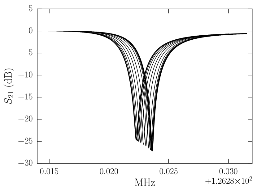
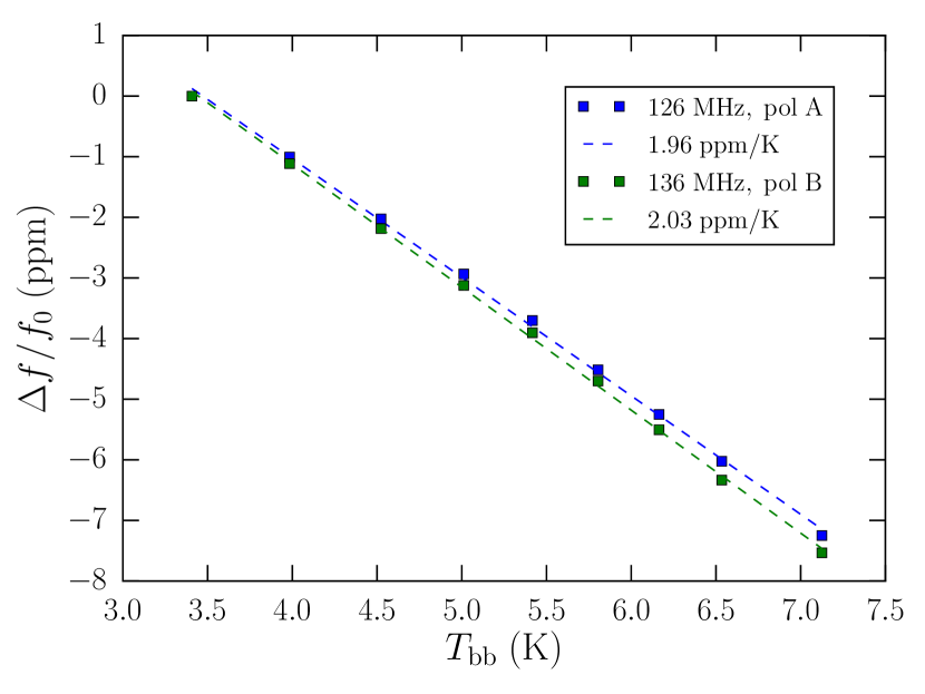
We measured the responsivity of the detectors with the blackbody load, where is the blackbody temperature. The absorbed power can be related to by integrating the Planck equation over the spectral band. In the regime above 3 K the relationship between and is approximately linear. At low the relationship between and is linear. At high , (Flanigan et al., 2016) and therefore .
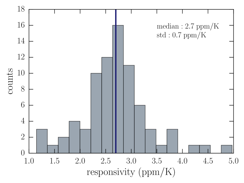
The fractional frequency shift is plotted as a function of for both detectors in a single array element in Fig. 6a. The blackbody temperature is stepped from 3.4–7.0 K. We find the data for both polarizations is well fit by a line with a slope of approximately 2 ppm/K, which is the responsivity. Across the array, the median responsivity is 2.7 ppm/K with a standard deviation of 0.7 ppm/K as shown in Fig. 6c. Previous iterations of dual-polarization detectors with straight inductors and smaller inductor volumes had responsivities between 12 and 16 ppm/K (McCarrick et al., 2016). The increase in inductor volume with the wiggled design has effectively lowered the responsivity and increased the dynamic range (more in Sec. 3.6).
3.3 Noise spectra and NET
We measured the noise properties of the detectors by recording TOD with the probe-tone frequencies fixed at the resonance frequencies determined by measurements. The resonator model (Eq. 3) is used to transform the TOD into fluctuations in resonance frequency and dissipation . We then calculate the power spectral densities (PSD) for both the fractional frequency and dissipation fluctuations, which we refer to as and , respectively. In practice we use the fractional frequency data because it is more responsive than the dissipation data. The noise spectrum is fit to the model
| (4) |
where is the white-noise level, is the amplifier noise level, is the low-frequency noise knee, and corresponds to the high frequency roll off.
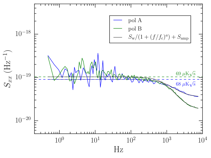
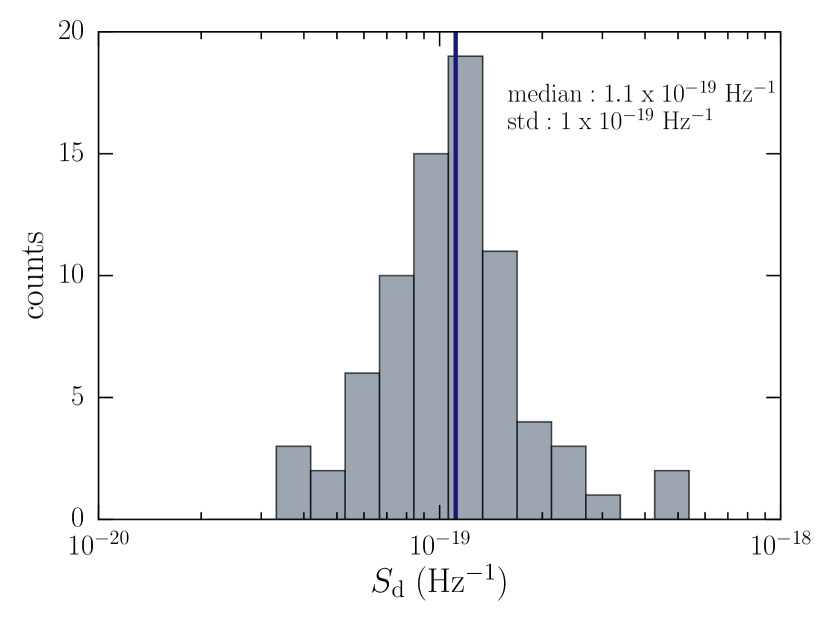
Typical measured detector noise spectra for both polarizations under a 3.4 K blackbody load are shown in Fig. 6b. Thirty seconds of TOD were collected with the sub-kelvin stage temperature regulated but the PTC off to eliminate mechanical vibrations. The module temperature was stable during the measurement but the radiation environment in the cryostat detectably changed. The noise spectra are therefore calculated from TOD detrended with a 2nd degree polynomial. The white noise levels for this detector pair are 5 and 9. We find that the noise spectra do not show detectable dependence in our measurements. TLS noise is expected to have a dependence (Noroozian et al., 2009), so any TLS noise in our devices would have an below 0.5 Hz. At high frequencies, the spectrum rolls off at approximately 700 Hz, which is consistent with the resonator bandwidth .
The noise equivalent temperature (NET) is calculated as
| (5) |
where the device noise level is defined as . The latter two terms are found by fitting Eq. 4 to the measured noise spectra. The factor of 1/ comes from the Nyquist sampling frequency. Taking the steps described in Sec. 3.2, we measure . We find that the NETs are 68 and 69 referenced to 3.4 K for the two polarizations as shown in Fig. 6b.
The median white noise level across the array is and the median device noise level is as shown in Fig. 6c. When fitting the noise spectra across the array, we use the frequencies above 100 Hz due to spikes at low frequencies in some resonators, which are caused by mechanical vibrations. To better understand how mechanical vibrations couple to the detector array, we took TOD from all of the detectors and conducted a spectral coherence analysis. We calculate the coherence estimator as , where and represent different detectors, and represents the cross spectrum of the fractional frequency fluctuations from two detectors. We initially found strong coherence in features across the bandwidth of the detectors. We hypothesized that the thickness of silicon wafer (160 m) in combination with the large surface area ( mm) caused the array to be sensitive to mechanical vibrations. To test this hypothesis, we installed the aforementioned spring-loaded pins in the module in an effort to suppress any vibrations in the substrate. After the spring loaded pins were installed, we found a large decrease in the coherence. However, there is still some detectable coherence below 100 Hz, which means the vibration suppression technique works but still needs further development.
3.4 Quasiparticle lifetime
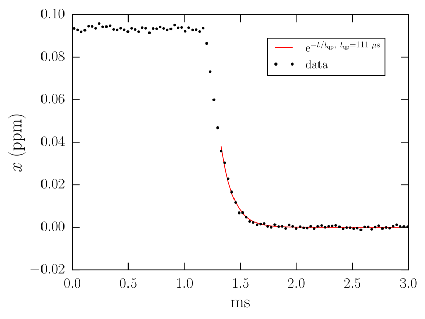
The quasiparticle lifetime was measured by taking TOD at a higher-order resonance ( GHz) while the detectors were illuminated by a constant 3.4 K blackbody background load and the external MMW source. It is necessary to use a higher-order resonance because the resonator ring-down time is , which is longer than for the 100 MHz resonances. For this test, the MMW source emits 148 GHz radiation, which transmits through the Eccosorb, and is switched on and off at 122 Hz with a PIN diode. The switching time of the PIN diode is fast (10 ns) compared to the LEKID response time, so any time constant associated with the MMW source is negligible. The TOD is then folded and averaged, the results of which are plotted in Fig. 7. The tail end of the falling edge of the averaged TOD is fit to an exponential model in order to estimate (Baselmans et al., 2017, 2008). The fit yields s.
3.5 Crosstalk
We define crosstalk as the response of a detector to a mechanism other than the absorption of radiation from its associated horn. The crosstalk is measured with all horns but one covered with aluminum tape, leaving a single array element (one LEKID pair) illuminated. The array is illuminated by the same chopped MMW source and background load as described in Sec. 3.4. In practice, we quantify the crosstalk as the relative response of each dark detector to that of the illuminated pair. All the detectors, both illuminated and dark, are simultaneously read out. At the highest incident power levels the MMW source can emit (where pW) the optical crosstalk is below dB, which suggests the RF choke works well.
3.6 Dynamic range
We determined the dynamic range of the detectors. The detectors were illuminated with both the blackbody source, from which we obtain as a function of , and the MMW source, from which we obtain as a function of , where is the power emitted by the MMW source. Thus, can be related to , and we can find an equivalent brightness temperature for the MMW source. This is advantageous because the MMW source can emit higher brightness temperatures than the blackbody, which starts to appreciably heat the sub-kelvin stage for K.
The quality factor and noise of the detectors are measured as a function of brightness temperature from the MMW source. Two metrics are used for the dynamic range: (i) the remains sufficiently high for the multiplexing requirements and (ii) the detector noise remains clearly elevated above the amplifier noise in the noise spectra. The detector noise remains separated from the amplifier noise, up to the highest brightness temperature of the MMW source, which is equivalent to approximately 90 K. Similarly, we find that , the minimum required for the desired multiplexing factor, for all accessible . For instance, for one resonator, changes from to , while decreases from to over the entire range. This puts a lower limit on the maximum brightness temperature the detectors can observe at 90 K.
3.7 NEP
We measured the absorbed noise equivalent power (NEP) as a function of absorbed power using the method from Flanigan et al. (2016). The detectors were illuminated through the Eccosorb by coherent radiation at 148 GHz from the MMW source. The source power was varied and at each power level we measured the detector noise and the fractional frequency shift . We numerically calculated to determine the desired responsivity. Experimentally, the NEP as referenced to the source is calculated as
| (6) |
where is the white noise level obtained by fitting Eq. 4 to the measured noise spectrum.
The theoretical NEP in the photon-noise limited case is
| (7) |
where is the absorbed power, is the superconducting energy gap, is the photon occupancy number and is the pair-breaking efficiency of the absorbed radiation. The first two terms are inherently due to photons and are respectively called the shot noise and the wave noise. Coherent radiation will produce only shot noise. The third term is due to the quasiparticle recombination rate and is referred to as recombination noise. We rewrite the theoretical NEP as referenced to the source as
| (8) |
where is the absorption efficiency of the detector as referenced to the MMW source power. Here, we have made the substitutions (de Visser et al., 2015) and , where is the bandwidth of incident radiation. We have also added in a constant term which refers to the limiting NEP.
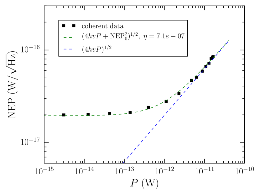
For one representative detector, we fit the coherent data as referenced to the source power to the expected model. Using GHz, we find . We use the parameter to calculate the absorbed NEP as a function of absorbed power , which is plotted in Fig. 7. We see when pW, signifying that the detector is photon-noise limited and detecting shot noise from the coherent radiation. The limiting level is approximately , similar to the NEP expected from a 3 K load.
3.8 Polarization response
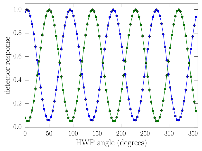
The polarization selectivity of the devices was characterized using a stepped HWP measurement, as is schematically depicted in Fig. 4. Purely linearly polarized MMW radiation is brought into the cryostat on a WR6 waveguide. This signal is then emitted from a conical horn and the emitted beam passes through the HWP, which is mounted directly in front of the horn aperture. The HWP is rotated in steps through one full rotation. At each orientation we measured the fractional frequency response and found that the response showed four cycles of a sinusoid for every rotation of the HWP as expected (see Fig. 8a) (Johnson et al., 2007). The measured polarization fraction (PF) is defined as
| (9) |
Here, corresponds to the intensity of the harmonic and corresponds to the intensity of the harmonic as computed by the discrete Fourier transform (DFT). We are able to calculate the intensity of the harmonics using a DFT as the measurements are taken at evenly spaced intervals over a complete period. For a single frequency at 147 GHz, we find the PF is approximately 89%. We expect this PF to be a lower bound on the polarization selectivity as we do not correct for cross-polarization induced in the setup, such as from the HWP or conical horns.
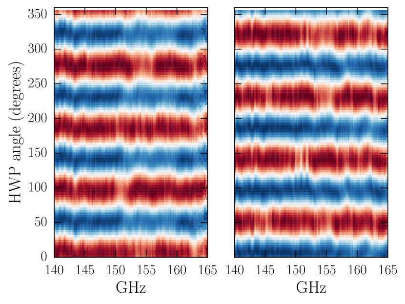
To measure the PF as a function of frequency, at each HWP orientation the incident MMW radiation frequency is swept from 140–165 GHz in 195 MHz steps. The results are plotted in Fig. 8b. We clearly see the two detectors are out of phase by approximately across the spectral band, which is expected if the detectors are sensitive to orthogonal polarizations.
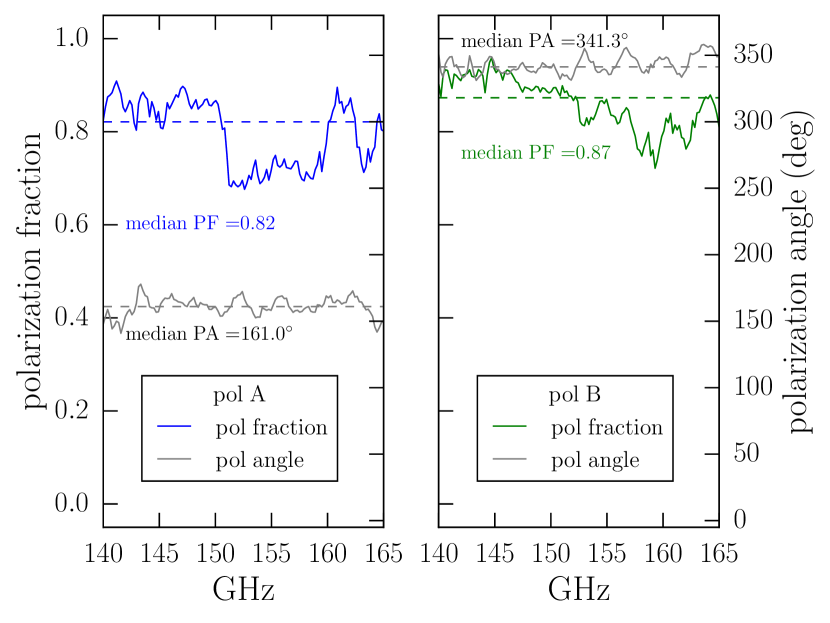
The response taken at the HWP angle that produced the maximum response is plotted at a function of incident MMW frequency in Fig. 8c. The median polarization fraction is 82% and 87% for polarizations A and B, respectively. The detectors are sensitive to orthogonal polarizations and have median responses out of phase corresponding to a polarization angle of .
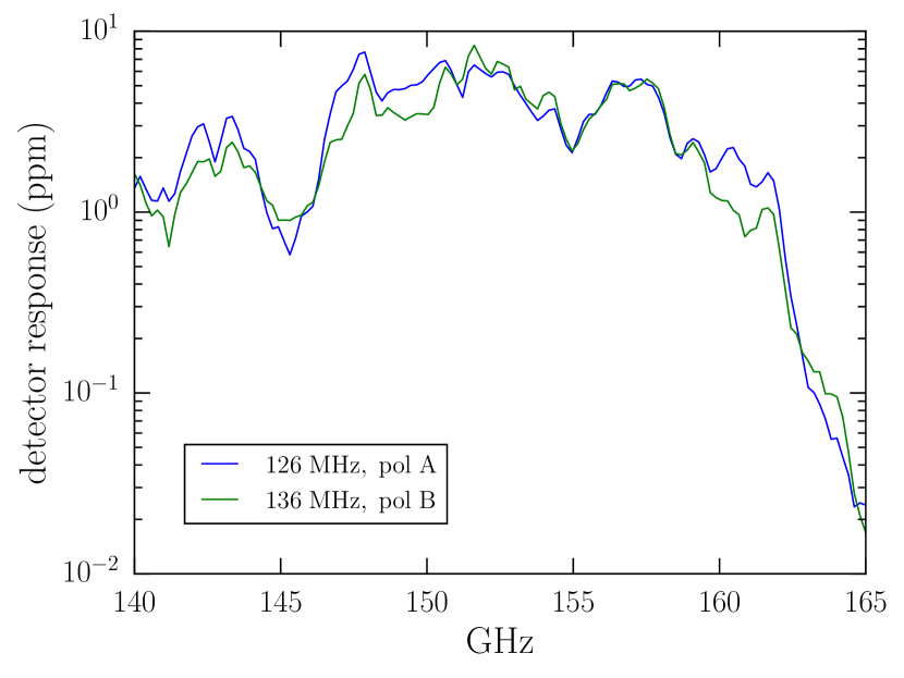
The spectral response of a pair of detectors fed by the same horn is plotted in Fig. 8d. The maximum response is taken at each incident MMW frequency. The response of both polarizations is similar across the entire MMW band. It is likely that the small scale structure in the spectral response is a systematic effect caused by the MMW source and reflections in the experimental setup.
4 Discussion
Future CMB experiments will require additional spectral bands and this dual-polarization LEKID design is directly scalable to other frequencies. While aluminum is sufficient for frequencies of 100–300 GHz, other materials can be used with the same design for both lower and higher spectral bands. For instance, materials such as aluminum manganese with a gap energy suitable for photons with frequencies GHz are currently being demonstrated (Jones et al., 2017). For higher frequency bands, like FIR, materials such as TiN are routinely used (Hailey-Dunsheath et al., 2016; Diener et al., 2012; Dober et al., 2016). Arrays of our design, scaled and fabricated with different materials, could be used to cover the entire bandwidth necessary to fully characterize the CMB and galactic foregrounds. The same design with small modifications could also be used for millimeter-wave observations from space. We expect approximately 0.3 pW of loading in space as compared to approximately 10 pW at ground-based observatories (Johnson et al., 2015). The lower loading conditions would require only a change to the inductor volume to tune the response and dynamic range.
In these tests we have demonstrated a multiplexing factor of 128, the number of detectors that can fit on the 100 mm diameter substrate. When populating a focal plane, up to 4 arrays can be tiled and connected so only a single pair of cables and one ROACH-based readout is needed for a multiplexing factor of 512. For this multiplexing scheme, each array in the focal plane would have detectors with unique resonance frequencies within the readout bandwidth.
We are working on a number of related projects. First, the number of detectors per array is being increased. For the higher detector density, we have designed and fabricated hex-packed arrays of dual-polarization LEKIDs fabricated on 100 mm silicon wafers with a 4.8 mm pitch. This detector density allows for 542 resonators per module. We are in the early stages of testing these arrays. Second, we are developing dual-polarization LEKIDs, which could be used for terrestrial imaging. The terrestrial imaging detectors are the same design as presented in this paper but with a larger absorbing volume achieved by increasing the film thickness. Third, we are considering ways to use these detectors for other ground-based, millimeter-wave astrophysical studies such as observations of star forming regions and the Sunyaev-Zel’dovich effect (Svoboda et al., 2016; Abazajian et al., 2016).
Subsequent iterations of the dual-polarization modules will further optimize the optical coupling scheme. The horns should either be profiled, the baseline design for these detectors going forward, or corrugated. For expediency, conical horns were used in the tests outlined in this paper. The optical coupling will be improved with either of these horn designs. Thermal contractions can cause optical misalignment in the array. HFSS simulations show misalignment can reduce optical efficiency while also increasing cross-polarization. Although we cannot probe the efficacy of the current alignment method (edge alignment) future iterations could use a pin and slot method which may better constrain the motion of the array.
The detector yield and the uniformity of the resonance frequency spacing could be increased. Currently, the detector yield is greater than 75%, however this should be able to reach close to 100%. Non-uniformities in the device metal could cause resonance frequencies to shift or opens in the resonator circuits. Some of the 160 m thick wafers have cracked during cryogenic cycling, so we are developing ways to make the arrays more mechanically robust by, for example, bonding them to thick handle wafers.
5 Conclusion
The dual-polarization LEKID array we have demonstrated in this study is the first for millimeter wavelengths and the first optimized for ground-based CMB polarization studies. In this paper, we have presented the design and characterization of the dual-polarization LEKIDs. The array of LEKIDs optimized to observe a 150 GHz spectral band is comprised of detector pairs sensitive to two orthogonal polarizations. The detectors have high internal quality factors which reach . The detectors are shown to have low-noise with an NET ¡ 100 under a 3.4 K load for the two polarizations. The detectors have uniform response between polarizations. The detectors have a large dynamic range and were not saturated up to a brightness temperature of 90 K. We demonstrate that the detectors have low crosstalk, below dB. We demonstrate that within a single element, the LEKIDs sensitive to orthogonal polarizations have high polarization selectivity for millimeter-wave radiation at 82% and 87% across the 140–165 GHz band. We show that the detectors are photon-noise limited above 1 pW of absorbed power.
The entire array is read out on a single coaxial line and the 128 multiplexing factor is higher than commonly used by current CMB experiments. The detectors and readout are designed to be straightforwardly increased to a multiplexing factor of 512. Additionally, the detectors are fabricated from a single layer of aluminum. The relatively simple fabrication process is a crucial strength of these devices as the next generation of CMB experiments will need a large increase in detector count. These results show that the dual-polarization LEKIDs are ready for an on-sky demonstration in a ground-based CMB polarimeter.
Acknowledgements.
We acknowledge the JPL Microdevices Lab, where the devices were fabricated, ASU, where the horn array was machined, and Cardiff University, where the filters were made. This work is partially funded by the Office of Naval Research. H. M. is supported by a NASA Earth and Space Sciences Fellowship. We thank A. Kerelsky for taking the photomicrographs in Figs. 1b and c. We thank the Xilinx University Program for their donation of the FPGA hardware and software tools that were used in the readout system.References
- Abazajian et al. (2016) Abazajian, K. N., Adshead, P., Ahmed, Z., et al. 2016, ArXiv e-prints [arXiv:1610.02743]
- Abitbol et al. (2017) Abitbol, M. H., Ahmed, Z., Barron, D., et al. 2017, ArXiv e-prints [arXiv:1706.02464]
- Adam et al. (2017) Adam, R., Adane, A., Ade, P. A. R., et al. 2017, ArXiv e-prints [arXiv:1707.00908]
- Adam et al. (2014) Adam, R., Comis, B., Macías-Pérez, J. F., et al. 2014, A&A, 569, A66
- Baselmans et al. (2017) Baselmans, J., Bueno, J., Yates, S. J. C., et al. 2017, A&A, 601, A89
- Baselmans et al. (2008) Baselmans, J., Yates, S. J. C., Barends, R., et al. 2008, J. Low Temp. Phys., 151, 524
- Bryan et al. (2015) Bryan, S., Bradford, K., Che, G., et al. 2015, ArXiv e-prints [arXiv:1503.04684]
- Bueno et al. (2016) Bueno, J., Yurduseven, O., Yates, S. J. C., et al. 2016, in 2016 41st International Conference on Infrared, Millimeter, and Terahertz waves, 1–2
- Calvo et al. (2016) Calvo, M., Benoît, A., Catalano, A., et al. 2016, J. Low Temp. Phys., 184, 816
- Day et al. (2003) Day, P. K., LeDuc, H. G., Mazin, B. A., Vayonakis, A., & Zmuidzinas, J. 2003, Nature, 425, 817
- de Visser et al. (2015) de Visser, P. J., Yates, S. J. C., Guruswamy, T., et al. 2015, Appl. Phys. Lett., 106, 252602
- Diener et al. (2012) Diener, P., Leduc, H. G., Yates, S. J. C., Lankwarden, Y. J. Y., & Baselmans, J. J. A. 2012, J. Low Temp. Phys., 167, 305
- Dober et al. (2016) Dober, B., Austermann, J. A., Beall, J. A., et al. 2016, J. Low Temp. Phys., 184, 173
- Doyle et al. (2008) Doyle, S., Mauskopf, P., Naylon, J., Porch, A., & Duncombe, C. 2008, J. Low Temp. Phys., 151, 530
- Flanigan et al. (2016) Flanigan, D., McCarrick, H., Jones, G., et al. 2016, Appl. Phys. Lett., 108
- Grayson et al. (2016) Grayson, J. A., Ade, P. A. R., Ahmed, Z., et al. 2016, in Proc. SPIE, Vol. 9914, Millimeter, Submillimeter, and Far-Infrared Detectors and Instrumentation for Astronomy VIII, 99140S
- Hailey-Dunsheath et al. (2016) Hailey-Dunsheath, S., Shirokoff, E., Barry, P. S., et al. 2016, J. Low Temp. Phys., 184, 180
- Harrington et al. (2016) Harrington, K., Marriage, T., Ali, A., et al. 2016, in Proc. SPIE, Vol. 9914, Millimeter, Submillimeter, and Far-Infrared Detectors and Instrumentation for Astronomy VIII, 99141K
- Henderson et al. (2016) Henderson, S. W., Stevens, J. R., Amiri, M., et al. 2016, in Proc. SPIE, Vol. 9914, Millimeter, Submillimeter, and Far-Infrared Detectors and Instrumentation for Astronomy VIII, 99141G
- Hubmayr et al. (2015) Hubmayr, J., Beall, J., Becker, D., et al. 2015, Appl. Phys. Lett., 106, 073505
- Janssen et al. (2013) Janssen, R. M. J., Baselmans, J. J. A., Endo, A., et al. 2013, Appl. Phys. Lett., 103, 203503
- Johnson et al. (2007) Johnson, B. R., Collins, J., Abroe, M. E., et al. 2007, ApJ, 665, 42
- Johnson et al. (2016) Johnson, B. R., Flanigan, D., Abitbol, M. H., et al. 2016, in Proc. SPIE, Vol. 9914, Millimeter, Submillimeter, and Far-Infrared Detectors and Instrumentation for Astronomy VIII, 99140X
- Johnson et al. (2015) Johnson, B. R., Vourch, C. J., Drysdale, T. D., et al. 2015, JAI, 4, 1550007
- Jones et al. (2017) Jones, G., Johnson, B. R., Abitbol, M. H., et al. 2017, Appl. Phys. Lett., 110, 222601
- Kamionkowski et al. (1997) Kamionkowski, M., Kosowsky, A., & Stebbins, A. 1997, Phys. Rev. D, 55, 7368
- Khalil et al. (2012) Khalil, M. S., Stoutimore, M. J. A., Wellstood, F. C., & Osborn, K. D. 2012, J. Appl. Phys., 111, 054510
- Knox & Song (2002) Knox, L. & Song, Y.-S. 2002, Phys. Rev. Lett., 89, 011303
- Mauskopf et al. (2014) Mauskopf, P. D., Doyle, S., Barry, P., et al. 2014, J. Low Temp. Phys., 176, 545
- Mazin et al. (2013) Mazin, B. A., Meeker, S. R., Strader, M. J., et al. 2013, PASP, 125, 1348
- McCarrick et al. (2016) McCarrick, H., Abitbol, M. H., Ade, P. A. R., et al. 2016, in Proc. SPIE, Vol. 9914, Millimeter, Submillimeter, and Far-Infrared Detectors and Instrumentation for Astronomy VIII, 99140O
- McCarrick et al. (2014) McCarrick, H., Flanigan, D., Jones, G., et al. 2014, Rev. Sci. Instrum., 85, 123117
- Noroozian et al. (2012) Noroozian, O., Day, P. K., Eom, B. H., Leduc, H. G., & Zmuidzinas, J. 2012, IEEE Transactions on Microwave Theory and Techniques, 60, 1235
- Noroozian et al. (2009) Noroozian, O., Gao, J., Zmuidzinas, J., LeDuc, H. G., & Mazin, B. A. 2009, in AIP Conf. Proc., ed. B. Young, B. Cabrera, & A. Miller, Vol. 1185, 148–151
- Posada et al. (2016) Posada, C. M., Ade, P. A. R., Anderson, A. J., et al. 2016, in Proc. SPIE, Vol. 9914, Millimeter, Submillimeter, and Far-Infrared Detectors and Instrumentation for Astronomy VIII, 991417
- Seljak & Zaldarriaga (1997) Seljak, U. & Zaldarriaga, M. 1997, Phys. Rev. Lett., 78, 2054
- Stebor et al. (2016) Stebor, N., Ade, P., Akiba, Y., et al. 2016, in Proc. SPIE, Vol. 9914, Millimeter, Submillimeter, and Far-Infrared Detectors and Instrumentation for Astronomy VIII, 99141H
- Svoboda et al. (2016) Svoboda, B. E., Shirley, Y. L., Battersby, C., et al. 2016, ApJ, 822, 59
- Swenson et al. (2012) Swenson, L. J., Day, P. K., Dowell, C. D., et al. 2012, in Proc. SPIE, Vol. 8452, Millimeter, Submillimeter, and Far-Infrared Detectors and Instrumentation for Astronomy VI, 84520P
- Szypryt et al. (2014) Szypryt, P., Duggan, G. E., Mazin, B. A., et al. 2014, MNRAS, 439, 2765
- Zmuidzinas (2012) Zmuidzinas, J. 2012, Annu. Rev. Condens. Matter Phys., 3, 169