Nano-Diamond Thin Film Field Emitter Cartridge for Miniature High Gradient Radiofrequency -band Electron Injector
Abstract
The complete design, fabrication, and performance evaluation of a compact, single cell, -band (9 GHz) electron injector based on a field emission cathode (FEC) are presented. A pulsed electron beam is generated by a 10’s of kW radiofrequency (RF) magnetron signal from a plug-in thin film nitrogen-incorporated ultrananocrystalline diamond (N)UNCD FEC cartridge. Testing of the -band injector with the (N)UNCD FEC was conducted in a beamline equipped with a solenoid, Faraday cup and imaging screen. The results show that typically the (N)UNCD FEC cartridge produces 1 mA/cm2 at a surface electric field of 28 MV/m. The diameter of the output beam generated from the 4.4 mm diameter (N)UNCD cartridge can be as small as 1 mm. In terms of its practical applications, the demonstrated -band electron injector with the (N)UNCD plug-in FEC can serve as a source for X-ray generation, materials processing, travelling-wave tubes (including GHz and THz backward wave oscillators), or can be used to drive slow-wave accelerating structures. The results presented also suggest that this field emitter technology based on planar (N)UNCD thin films, which are simply grown on the surface of optically polished stainless steel, can enable a vast number of device configurations that are efficient, flexible in design, and can be packaged with ease.
Radiofrequency (RF) electron guns that drive industrial, medical and scientific accelerators typically use electric fields in excess of 10-20 MV/m, applied to the cathode surface. This is to mitigate space-charge effects for efficient beam transport and downstream staged acceleration, or to produce high energy electrons for efficient interaction with slow-wave structures in vacuum electronics devices. A number of accelerator applications require high brightness, highly coherent beams (free electron lasers) making use of photocathodes, or high current beams (synchrotrons, industrial electron beam processing and cargo inspection facilities) making use of thermionic emitters. Field emission cathodes (FECs) could occupy a niche in which moderate beam currents are needed, and/or in which simplicity and compactness of the electron injection system (as compared to laser-photocathode concept) and/or fast ON/OFF switching (as compared to slow thermionic sources) is a must. Therefore, some efficient, simple and scalable in design and fabrication electron field emission source would be needed for high gradient injection, and the search is ongoing [1-4].
Compared to thermionic and photoemission cathodes, FECs have kept a relatively low application profile. Development of a vast number of FECs based on metallic and semiconductor whiskers/wires [5], pillars [6], tips [7] etc. did lead to a limited number of high power [8, 9] or high speed devices [10, 11] and other applications of field emitters [11]. Even so, the major progress to date in device fabrication and commercialization was achieved using only one field emitter platform, the proprietary molybdenum Spindt cathodes developed and manufactured at Stanford Research Institute [11, 13]. The standard problems remain the same: geometrical inhomogeneity of emitters in the array and fabrication complexity that make scalable FEC production challenging. Carbon-derived materials such as carbon nanotubes (CNTs), on the other hand, have gained greater attention as field emission sources. They are simple to synthesize on various substrates of various form factors and their synthesis can be scaled. Although CNTs have proven to be remarkable FECs [14], the applied macroscopic electric fields have to be maintained in the range below 10 MV/m because CNTs (like any other sharp emitters) have an extremely high aspect ratio leading to a large geometrical enhancement factor , on the order of 1,000. High aspect ratio structures with 1,000 can be impaired or disrupted when placed in an external electric field larger than 10 MV/m, because the product of the external macroscopic electric field multiplied by , called the local electric field, sets the ultimate field limit a solid state material can physically sustain; this ultimate field is 10 V/nm [15, 16]. Of course, the field emitter failure is also heavily dependent on the local current density through the emitter, but the rough magnitude of the external macroscopic electric field applied to a field emitter can frequently be estimated as less than or on the order of . This limiting factor precludes CNT FECs from use as electron sources in high gradient electron injectors.
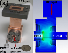
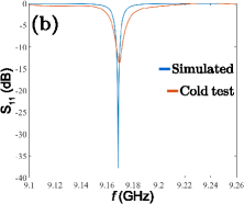
Previously, it was established that some other carbonic materials, such as amorphous carbons and polycrystalline diamond, e.g., in the form of nano-crystalline and ultra-nano-crystalline diamond can be effective field emitters in the planar thin film configuration [17, 18]. More specifically, nitrogen-incorporated ultrananocrystalline diamond ((N)UNCD) field emitters have long life times [19] and low turn-on macroscopic fields 10 MV/m [18, 20]. Thin film (N)UNCD FEC can be operated at electric fields 10 MV/m, i.e. in the field range that is complementary to that of CNTs, and make (N)UNCD attractive for high gradient electron injector technology. Following our previous proof-of-concept experiments with -band 1.3 GHz MW-class electron injectors [3], we now present results on the performance of a (N)UNCD planar field emitter installed in a custom, miniature -band 9.17 GHz, kW-class injector driven by a conventional RF magnetron delivering 60 kW of power which produced up to 28 MV/m surface gradient. The reason for the choice of this application case is two-fold. First to demonstrate the scalability of the injection concept that relies on the (N)UNCD FEC by making a complete and properly working device miniaturized 10-fold as compared to -band type injectors [3]. Second, to demonstrate that (N)UNCD plug-in FEC is a technology that can enable fabrication, commissioning and operation of most miniature electron guns in the RF electron injector family (e.g. -band spans 8-12 GHz, while the RF gun size is inversely proportional to the operating frequency ). In this case, size constraints on the use of laser injection or high temperature heater installation can be fully avoided. The injector presented here has a conventional single-cell quarter-wave design. It combines a copper body that stores the energy of the RF field with stainless steel flanges. Circular standard 1.33” conflat type flanges at the front and the back of the injector provide for vacuum beamline connections and cathode plug insertion. A CERN type rectangular flange provides for vacuum/RF connection. The copper and stainless steel parts were brazed together. Fig.1a illustrates the final injector assembly together with the cathode plug, and the simulated electric field distribution. Fig.1b shows the simulated versus measured -parameter (input port reflection). The measurement was made in a blanked cold test, i.e. a cold test of the empty cavity with no cathode installed. Its fundamental frequency was found to be 9.17 GHz.
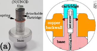
The full cathode plug assembly is shown in Fig.2. It consists of a base with a venting hole on the back. The cartridge made of stainless steel (SS) is attached to the base with a set screw. At the joint location, there is a groove that holds a spring, the standard technique for enabling good RF contact between the cathode plug and the body of the injector. The SS cartridge was mirror polished and coated with Mo. Subsequently the (N)UNCD thin film was deposited using the standard microwave-plasma assisted CVD process [3].
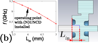
Upon installation, the length of the cartridge inside the cavity determines the operating frequency by changing the effective size of the cavity volume seen by the RF drive signal. The total length of the cathode plug tip with the cartridge atop is precisely machined. From the known geometry, simulations and cold testing, we can relate the final frequency as measured with a network analyzer to the length of the cartridge inside the cavity, which cannot be directly measured. This is an important correlation because it affects the distance between the (N)UNCD field emitter and the exit aperture plane and thus the ultimate energy gain of the output electrons (product of on-axis electric field and distance). In Fig.2b, the resonance frequency is plotted against the cartridge length inside the copper injector cavity, the parameter. The way the length is defined is depicted on the right panel of Fig.2b. The final cathode plug design, when fully assembled and installed with the 1.33” flange tightened, leads to =4 mm, thus fixing the operating frequency at 9.17 GHz. The full set of the key parameters that describe the performance of the injector are summarized in Table 1.
Table 1. The simulated and measured fundamental parameters of the fabricated cavity with the (N)UNCD/Mo/SS cartridge installed: is the cavity quality factor, is the quality factor of the whole injector assembly that includes RF window and waveguide losses.
| simulation | cold test | |
| (GHz) | 9.1697 | 9.1694 |
| 2286 | 800 | |
| 2285 | 1218 | |
| =/ | 1.00 | 0.66 |
| / | 4.3 | n/a |
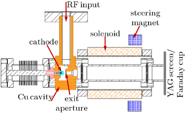
Fig.3 shows the full beamline layout. The entire beamline assembly is located on top of an oil-free hybrid diaphragm/turbo pump station. The working pressure in the beamline is Torr. The beamline consists of:
1. The cavity connected to the magnetron through an -band RF window, which is an RF transparent septum between the vacuum volume of the cavity and ambient pressure waveguide from the magnetron;
2. The solenoid installed outside the vacuum pipe directly at the cavity exit to focus the exiting beam;
3. Specialty in vacuum YAG:Ce screen, or a Faraday cup with a telescopic electrode which can collect electrons either at the YAG:Ce screen position or directly at the injector exit aperture. Only the YAG:Ce screen or the Faraday cup can be installed at a given time at the end of the beamline, with either detector serving also as a beam dump;
4. Steering magnet at the exit plane of the solenoid to steer the beam in the transverse plane across the YAG screen to measure the beam energy.
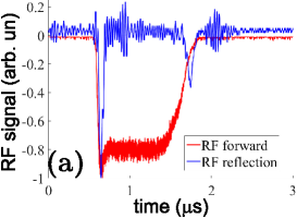
The magnetron produces a 1 s macroscopic pulse (Fig.4a) consisting of 9.17 GHz oscillations at a power of up to 250 kW. The RF power is split with a 6 dB splitter, so that the maximum power available in our experiment is 57 kW. Using the values of the injector parameters listed in Table 1, the input magnetron power can be converted into the electric field on the cathode surface as
where stands for experiment, stands for simulation, and stands for input.
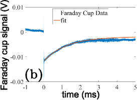
The RF pulse in Fig.4a demonstrates the typical behavior: two sharp RF reflection features at the beginning and the end of the pulse related to filling with and emptying the cavity of RF energy. Fig.4b shows temporal profile of a Faraday cup signal. A standard measurement circuit with a time constant of 1 ms was used. The actual full charge (measured in C) per 1 s RF macroscopic pulse extracted from the cathode and transported through the exit aperture is given by
where is the scope trace of voltage vs time, and is the resistor value equal to 1 M (with capacitor value of 1 nF).
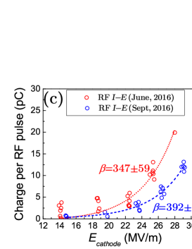
Finally, using Eqs. (1) and (2) we obtain the dependence of the charge per RF pulse versus , as shown in Fig.4c. The cathode was tested over a three month period with the cathode performing under high electric field for a total of two weeks continuously at a 10 Hz repetition rate. Data were taken at 1 Hz. Fig.4c represents data from the first and the last runs. As can be seen, the cathode was conditioned to up to 28 MV/m, and a charge per RF pulse of 20 pC was achieved which translates into a current of 1 mA/cm2 per RF pulse, if, as before [3], it is assumed that emission is triggered over around the RF electric field maximum (1/6 the duration of the positive part of the GHz oscillation) from the entire cartridge area. 20 pC per RF pulse implies electrons.
Referring to Fig.4c, the Faraday cup telescopic electrode measured similar values of charge per RF pulse when placed directly at the exit aperture of the injector or a few centimeters after the solenoid, with the solenoid current set to 8-10 A corresponding to about 140 Gauss on the -axis. With the solenoid settings determined, the Faraday cup was replaced with the in vacuum YAG:Ce screen assembled on the vacuum side of a conflat glass window with a camera placed behind the window. In this configuration no imaging distortions were introduced as all components were placed one after another and centered with respect to the beam propagation direction (-axis). Fig.5 summarizes the transverse (, ) beam profiles that were obtained at different solenoid settings. At 8.5 A, the beam profile had minimal size with an intense core of about 1 mm in diameter.

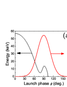
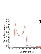
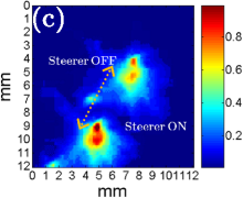
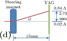
As before [3], we overlap launch phase dependences of the current and the energy gain in the gun (Fig.6a) to obtain the resulting energy spectrum of emitted electrons, as plotted in Fig.6b. The resulting energy spread is rather wide and spans 5 to 14 keV, as the cavity is not purposely optimized for better energy spread. With the solenoid set to 8.5 A, a horizontal scan was performed with a resulting shift illustrated in Fig.6c; current through the steering magnet was 0.82 A. Using the measured beam position shift on the YAG:Ce screen (2.75 mm) and the drift distance from the steering magnet to the YAG:Ce screen (15 mm), the beam energy was estimated equal to 10 keV (see Fig.6d for reference). The experimentally measured energy is in excellent agreement with the 9-10 keV central energy of the spectrum obtained from the semi-empirical calculations (Fig.6b). The following formula was used [21]
where , a sum of the kinetic and rest energy of the electron, is the total energy; is the ratio of electron velocity and the speed of light; = 61 Gcm was calculated from the field maps obtained from the steering magnet manufacturer at a bias current of 0.82 A. Because neither nor are known, Eq.(3) can be solved, e.g., graphically in order to deduce and hence . Note, the observed bimodal structure in the launch phase dependence, Fig.6a, translates into a bimodal structure in the energy spectrum and into the longitudinal bunch modulation. Due to slight asymmetry in the injector geometry design and because our imaging system is time integrating over a span of milliseconds, the longitudinal bunch modulation projects at different locations on the YAG:Ce screen (Fig.5 and Fig.6c). This effect does not reflect non-uniformity of electron emission from the cathode surface.
Built upon our previous results presented for the -band injector [3], the results presented here suggest that the technology of plug-in (N)UNCD FEC cartridges developed here enables simple electron gun devices. A miniature 9.17 GHz injector device delivering 1 mA/cm2 of current at 10 keV was designed, fabricated and commissioned. The same approach can be implemented for a wide range of electron injectors (e.g. -, -, - or - bands). This means that the proposed concept is essentially scalable and adaptive. The cartridges are disposable or can be recycled for (N)UNCD re-deposition. In the earlier work [3], it was demonstrated that (N)UNCD can survive and perform under fields as high as 40-65 MV/m. In present work, it is shown that (N)UNCD field emitters can, having a turn-on field around 5 MV/m, work at much lower gradients, from 14 to 28 MV/m. These observations let us conclude that the planar (N)UNCD field emitter can adapt, without disruption, to the electric field required for a specific application, starting at 10 MV/m (-factor 300-400) and higher (at least up to 70 MV/m, -factor 100), by irreversibly reducing its apparent originally high -factor [17, 18], such that the entire operating - curve is modified accordingly.
In engineering physics, copper resonant cavity injector technology is mature. If the field emission current enabled by (N)UNCD (with no laser or heaters required) is satisfactory for the application, a half-, single-, or multi-cell injector with RF input ports can be designed to meet specific requirements on the operating frequency, power consumption, duty cycle, beam kinetic energy and energy spread, and transverse phase space.
Acknowledgments
We thank Paul Schoessow for his help with the manuscript. Euclid was supported by the Office of Nuclear Physics of DOE through a Small Business Innovative Research grant No. DE SC 0013145. (N)UNCD synthesis and characterization work at Center for Nanoscale Materials, Argonne National Laboratory was funded by Office of Energy Efficiency & Renewable Energy, Advanced Manufacturing Office, Department of Energy Technology Commercialization Fund, under Agreement number 32138, Funding action number 69530. Use of the Center for Nanoscale Materials, an Office of Science user facility, was supported by the U.S. Department of Energy, Office of Science, Office of Basic Energy Sciences, under Contract No. DE-AC02-06CH11357.
References
- (1) X. Li, M. Li, L. Dan, Y. Liu, and C. Tang, Phys. Rev. AB 16, 123401 (2013).
- (2) P. Piot, C. A. Brau, B. K. Choi, B. Blomberg, W. E. Gabella, B. Ivanov, J. Jarvis, M. H. Mendenhall, D. Mihalcea, H. Panuganti, P. Prieto, and J. Reid, Appl. Phys. Lett. 104, 263504 (2014).
- (3) S. V. Baryshev, S. Antipov, J. Shao, C. Jing, K. J. Pérez Quintero, J. Qiu, W. Liu, W. Gai, A. D. Kanareykin, and A. V. Sumant, Appl. Phys. Lett. 105, 203505 (2014).
- (4) D. Mihalcea, L. Faillace, J. Hartzell, H. Panuganti, S. Boucher, A. Murokh, P. Piot, and J. C. T. Thangaraj, Appl. Phys. Lett. 107, 033502 (2015).
- (5) Y.-H. Lee, C.-H. Choi, Y.-T. Jang, E.-K. Kim, B.-K. Ju, N.-K. Min, and J.-H. Ahn, Appl. Phys. Lett. 81, 745 (2002).
- (6) C. Langer, C. Prommesberger, R. Lawrowski, R. Schreiner, P. Serbun, G. Mueller, F. D sberg, M. Hofmann, M. Bachmann, and A. Pahlke, J. Vac. Sci. Technol. B 34, 02G107 (2016).
- (7) P. Serbun, B. Bornmann, A. Navitski, G. Mueller, C. Prommesberger, C. Langer, F. Dams, and R. Schreiner, J. Vac. Sci. Technol. B 31, 02B101 (2013).
- (8) M. Garven, S. N. Spark, A. W. Cross, S. J. Cooke, and A. D. R. Phelps, Phys. Rev. Lett. 77, 2320 (1996).
- (9) D. R. Whaley, R. Duggal, C. M. Armstrong, C. L. Bellew, C. E. Holland, and C. A. Spindt, IEEE Trans. Electron. Devices 56, 896 (2009).
- (10) W. P. Kang, J. L. Davidson, A. Wisitsora-at, Y. M. Wong, R. Takalkar, K. Holmes, D. V. Kerns, Diamond Relat. Mater. 13, 1944 (2004).
- (11) D. Temple, Mater. Sci. Engineering R 24, 185 (1999).
- (12) C. A. Spindt, I. Brodie, L. Humphrey, and E. R. Westerberg, J. Appl. Phys. 47, 5248 (1976).
- (13) D. R. Whaley, B. Gannon, C. R. Smith, and C. A. Spindt, IEEE Trans. Plasma Sci. 28, 727 (2000).
- (14) W. A. de Heer, A. Chatelain, and D. Ugarte, Science 270, 1179 (1995).
- (15) D. Alpert, D. A. Lee, E. M. Lyman, and H. E. Tomaschke, J. Vac. Sci. Technol. 1, 35 (1964).
- (16) A. Grudiev, S. Calatroni, and W. Wuensch, Phys. Rev. ST Accel. Beams 12, 102001 (2009).
- (17) J. Robertson, J. Vac. Sci. Technol. B 17, 659 (1999).
- (18) R. G. Forbes, Solid State Electron., 45, 779 (2001).
- (19) S. A. Getty, O. Auciello, A. V. Sumant, X. Wang, D. P. Glavin, and P. R. Mahaffy, Proc. SPIE 7679, 76791N (2010).
- (20) M. L. Terranova, S. Orlanducci, M. Rossi, and E. Tamburri, Nanoscale 7, 5094 (2015).
- (21) A. W. Chao, K. H. Mess, M. Tigner, and F. Zimmermann, Handbook of accelerator physics and engineering (2012), see page 381.