Rate capability and magnetic field tolerance measurements of fast timing microchannel plate photodetectors
Abstract
Microchannel plate photodetectors provide both picosecond time resolution and sub-millimeter position resolution, making them attractive photosensors for particle identification detectors of a future U.S. Electron Ion Collider. We have tested the rate capability and magnetic field tolerance of 66 cm2 microchannel plate photodetectors fabricated at Argonne National Laboratory. The microchannel plate photodetector is designed as a low-cost all-glass vacuum package with a chevron pair stack of next-generation microchannel plates functionalized by atomic layer deposition. The rate capability test was performed using Fermilab’s 120 GeV primary proton beam, and the magnetic field tolerance test was performed using a solenoid magnetic with tunable magnetic field strength up to 4 Tesla. The measured gain of the microchannel plate photodetector is stable up to 75 kHz/cm2, and varies depending on the applied magnetic field strength and the rotation angle relative to the magnetic field direction.
Keywords: Fast timing, Microchannel plate, Photodetector, Electron Ion Collider, Particle identification detector, Rate capability, Magnetic field, Rotation angle.
1 Introduction
The world’s first Electron Ion Collider (EIC) [1] has been recommended in the 2015 Long Range Plan for Nuclear Science as the highest priority for a new facility construction in the U.S following the completion of the Facility for Rare Isotope Beams (FRIB) [2]. This unique facility will explore several features of the strong force and QCD by mapping the parton content, quarks and gluons, of nucleons and nuclei up to uranium through processes such as semi-inclusive deep inelastic scattering and exclusive deeply virtual Compton scattering.
Several detector concepts have been proposed and designed for the EIC at
Argonne National Laboratory (ANL), Brookhaven National Laboratory (BNL), and
Thomas Jefferson National Accelerator Facility (JLab). For all these EIC
detector designs, excellent particle identification (PID)
(///)
over a wide range of momentum is essential for the proposed measurements.
Time-of-flight systems and imaging C̆erenkov detectors, such as Ring Imaging
C̆erenkov (RICH) [3, 4] and Detection of Internally Reflected C̆erenkov light (DIRC) [5] detectors, are proposed. Both of these
detector classes are calling for large area, low cost photon sensors with high
spatial resolution, high rate capability, radiation tolerance, magnetic field
tolerance, and picosecond timing resolution.
Microchannel plate (MCP) photodetectors are compact photon sensors, usually with an internal chevron pair stack of MCPs. This geometry provides both high spatial and temporal resolution in a vacuum package. The Large Area Picosecond Photodetector (LAPPDTM) is the world’s largest MCP based photodetector with an active area of 2020 cm2 [6]. It is designed as a modular all-glass detector package with the next-generation MCPs produced by applying resistive and emissive coatings to borosilicate glass capillary array (GCA) substrates through atomic layer deposition (ALD). The all-glass design and low-cost next-generation MCPs provide great advantages in reducing the LAPPDTM product cost per area compared to other currently available MCP based photodetectors. As a collaborating group of the LAPPD project [7], we have built an MCP photodetector fabrication system [8] at ANL to fabricate 66 cm2 MCP photodetectors with LAPPD design. The ANL’s MCP photodetector fabrication system also serves as an R&D platform for LAPPD package design validation and optimization. Several 66 cm2 MCP photodetectors with standard LAPPD design were successfully fabricated at ANL and tested [9, 10, 11], exhibiting a high gain over 107, an overall time resolution of 35 ps, and a position resolution better than 1 mm. The excellent performance of these 66 cm2 MCP photodetectors shows that the low-cost LAPPDTM detector is a promising candidate photosensors for the EIC PID detector systems. Performance tests of the MCP photodetectors in high rate, high radiation damage, and high magnetic field environments are required to further validate the application of LAPPDTM detectors as the EIC PID photosensors.
In this paper, we describe the current design of 66 cm2 MCP photodetectors fabricated at ANL, report recent results on their performance tests in a high rate environment and a high magnetic field environment. The direction of further optimization of the LAPPDTM design for an EIC PID application is also addressed at the end of this paper.
2 Design of the MCP photodetector assembly
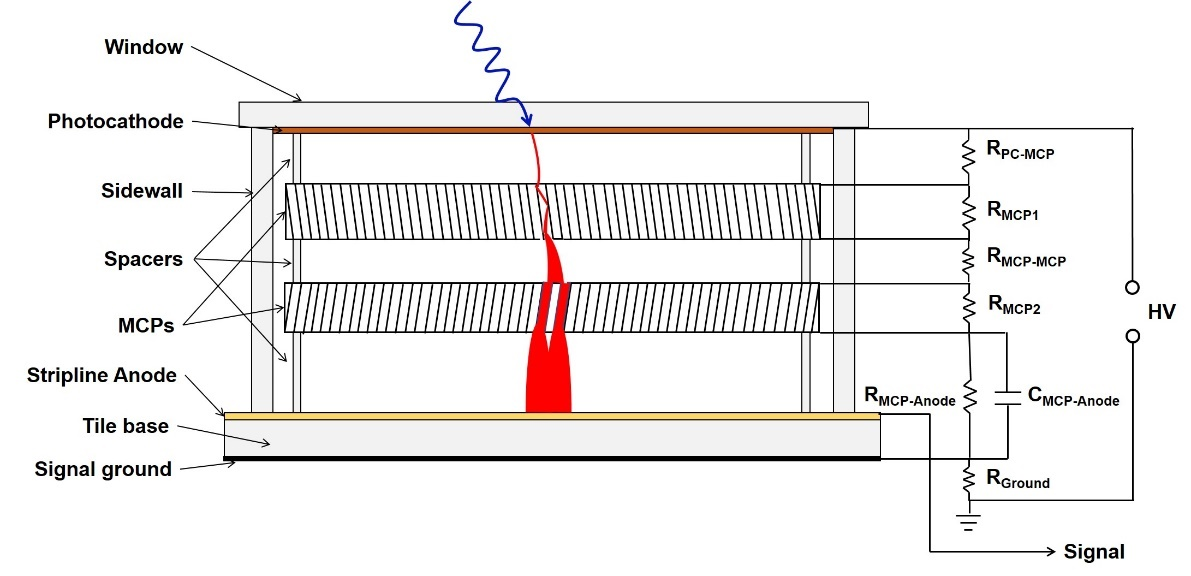
The current ANL design of the 66 cm2 MCP photodetector is developed from the original LAPPD internal resistor chain design [11], similar to the current commercial standard design of LAPPDTM detectors [12]. Figure 1 shows a schematic design of the current ANL MCP photodetector assembly and its electrical circuit diagram.
The MCP photodetector is an all glass body assembly, consisting of a glass base window, a top window, two side walls, three grid spacers and two MCPs. The side walls are frit-bonded onto the base window, with silver stripline anodes printed to lead the signals and high voltage connections to the outside. Three grid spacer sets are used; one between the top window and the upper MCP, one between the two MCPs, and one between the lower MCP and the anode. These spacers function as insulators to separate the different components, and also to hold these internal components in place in the vacuum assembly.
When light hits the photocathode, photoelectrons are emitted and are then accelerated towards the MCP hitting the inner wall of a channel and emitting secondary electrons. Then, the secondary electrons are further accelerated by the electric field generated across the ends of the MCP bombarding the channel wall again and producing additional secondary electrons. This process is repeated as the electrons travel along the channels of the MCPs. Two MCPs are used in our design to ensure that the electrons are multiplied several times, and the signals deposited onto the stripline anode are strong enough for signal detection.
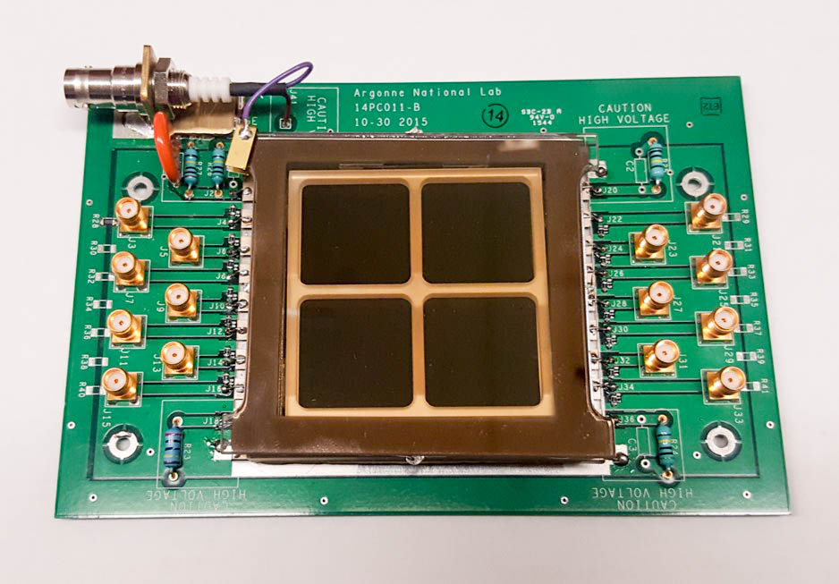
Four ultra-thin metal shims are applied at the top and bottom surfaces of the two MCPs to lead the electrical connection to external connections. The detailed description of the circuit connection inside the vacuum package can be found in reference [13]. This independent bias-voltage design provides the advantage of individually controlling and fine tuning the bias voltage for each MCP. A Bialkali photocathode is deposited on the inner surface of the top window, and an indium seal is made between the top window and the side wall through a low temperature thermo-compression sealing process to form a hermetic vacuum detector package. The completed MCP photodetector is attached to a custom-made circuit board, providing a permanent mount and firm electrical connections, as shown in Figure 2. External electrical connections for both signal and high voltage are inserted into the external resistor connections to serve as high voltage dividers, ensuring both MCPs work at an independently optimized high voltage for the best performance. Additional capacitors may also be added across the resistor divider for better signal waveform.
The microchannel plates used in the 66 cm2 MCP photodetector are diced from the next-generation large area (2020 cm2) MCPs [6, 12], the world’s largest commercially available MCPs. These next-generation MCPs are produced through a glass drawing process and functionalized through the ALD process. This is completely different from the production of traditional leaded glass MCPs. The glass drawing process uses borosilicate glass as the tube material, which is considerably less expensive than leaded glass and eliminates the chemical etching process required in the traditional method. This makes it much more cost-effective for MCP production. Here, we use standard borosilicate glass MCPs with 20 m pore size, 60:1 L/d (pore length to diameter) ratio and 8∘ bias angle relative to the MCP surface normal. The two MCPs are placed as the chevron configuration in the vacuum package, which reverses the bias angle to -8∘.
3 Rate capability measurement
The rate capability of MCP photodetectors is one of the most critical parameters for applications in high luminosity environments, such as an EIC. Due to the high resistive layer coating on ALD functionalized MCPs, the current in the MCP pores may not flow off fast enough when the MCP detector is exposed to high particle rates. This effect may cause severe charge saturation reducing the gain of the MCP photodetector, and limiting the detector performance.
We investigated the rate capability of the 66 cm2 MCP photodetectors with the 120 GeV/c primary proton beam at Fermilab Test Beam Facility (FTBF). As the protons travel through the 3 mm thick glass top window of the MCP photodetector, C̆erenkov light is produced and detected by the MCP photodetector as our signals. The beam is delivered as a slow spill with a 4 s duration once per minute with a maximum intensity of 105 particles per spill. The beam has an elliptical shape, a major-diameter of 4.6 mm and a minor-diameter of 1.8 mm, and a Gaussian density profile. The incident proton beam was monitored by an upstream multiwire proportional counter to see the beam profile. Three plastic scintillators were used in coincidence as a trigger and to count the number of incident protons. A light-tight dark box was designed to hold the MCP photodetector in the beam path with the detector surface facing the beam direction. High voltage was applied to the MCPs through an external resistor voltage divider, and signals from the striplines were read out through a DT5742 desktop digitizer [14] produced by CAEN (Costruzioni Apparecchiature Elettroniche Nucleari S.p.A.) with a sampling rate of 5 GS/s. The digitizer is based on a switched capacitor array of DRS4 (Domino Ring Sampler) chips [15], 16 analog input channels, and one additional analog input for fast trigger.
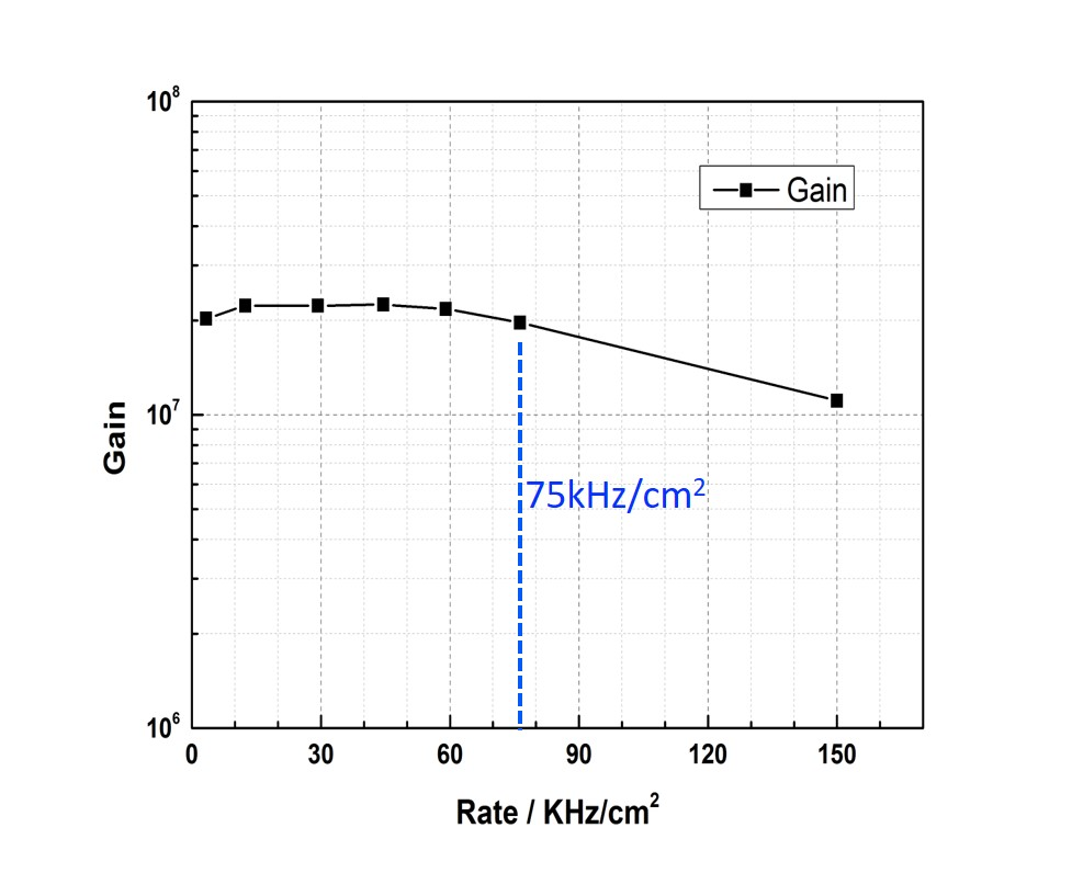
During our experiment, the 120 GeV/c proton beam intensity was tuned to vary from 500 to 40,000 particles per spill. The beam rate was calculated using the number of triggers per spill and was corrected for the size of the beam spot by reconstructing the beam profile. The calculated beam rate varied from 3 to 150 kHz/cm2 corresponding to the monitored beam particle intensity. Figure 3 shows the gain of the MCP photodetector measured as a function of the beam rate. The measured gain of the investigated detector is stable up to a beam flux of 75 kHz/cm2, and is still over 107 when the beam flux reaches 150 kHz/cm2. Such a high rate capability of the MCP photodetector will be sufficient for EIC PID detectors at the proposed beam energies.
4 Magnetic field tolerance measurement
In the EIC detector concepts, solenoid magnets with field strengths of 1.5 Tesla are proposed. The imaging C̆erenkov detectors (RICH, DIRC) and time-of-flight systems are designed to cover the area of the barrel and end caps for charged particle (///) separations. This compact design requires the photosensors to work properly in harsh environments with magnetic field strengths up to 1.5 Tesla.
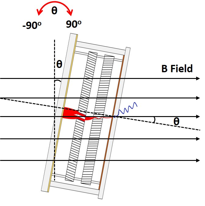
At ANL, a decommissioned superconducting magnet from a magnetic resonance imaging (MRI) scanner was acquired to test instruments for the muon experiment [16]. The magnet provides a large bore with a diameter of 68 cm and a very homogeneous field (7 ppb/cm), with a tunable strength of the magnetic field up to 4 Tesla. We have built a characterization system compatible with the solenoid magnet to test the performance of the 66 cm2 MCP photodetector in a strong magnetic field environment. The MCP photodetector was fixed in a custom built non-magnetic, light-tight dark box. The dark box was held on a test platform with the detector surface normal to the direction of magnetic field. The position of the dark box was adjusted so that the center of the MCP photodetector was well-aligned with the center of the solenoid magnet. A rotation mechanism was also integrated with the system, allowing rotation of the MCP photodetector with an angle , as shown in Figure 4. A 405 nm light-emitting diode (LED) was used as the light source and was introduced to the surface of the MCP photodetector through an optical fiber. High voltage was applied to the MCPs from a supply with variable voltage control, and signals from the striplines were read out through the CAEN DT5742 desktop digitizer.
4.1 Magnetic field strength dependence
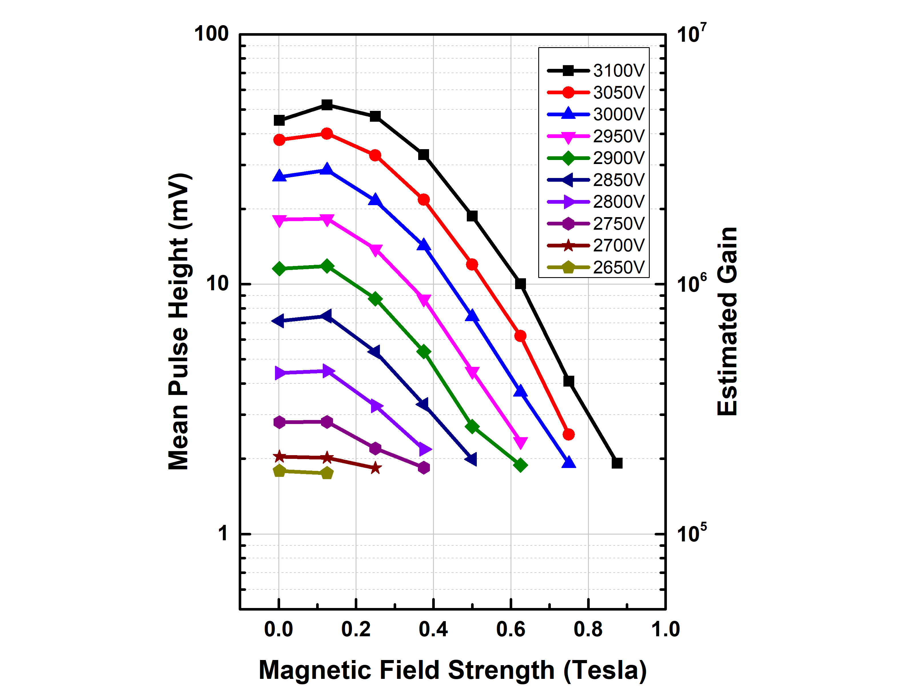
The dependence of the MCP photodetector performance on the magnetic field strength was done at a rotation angle = 0∘, i.e., where the direction of the magnetic field is normal to the surface of the MCP photodetector. We measured the performance of the investigated MCP photodetector in various magnetic field strengths at different bias high voltages. The results are presented in Figure 5. At a fixed bias high voltage, the mean pulse height of the MCP photodetector increases slightly as the magnetic field strength increases to 0.2 T, decreases as the magnetic field strength continues to increase, and eventually breaks down at a fixed magnetic field strength of 0.8 T. In the same magnetic field environment, the mean pulse height of the MCP photodetector increases as the high voltage increases. This behavior is similar to our previous measurements of the MCP photodetectors without applying a magnetic field [10].
4.2 Magnetic field angle dependence
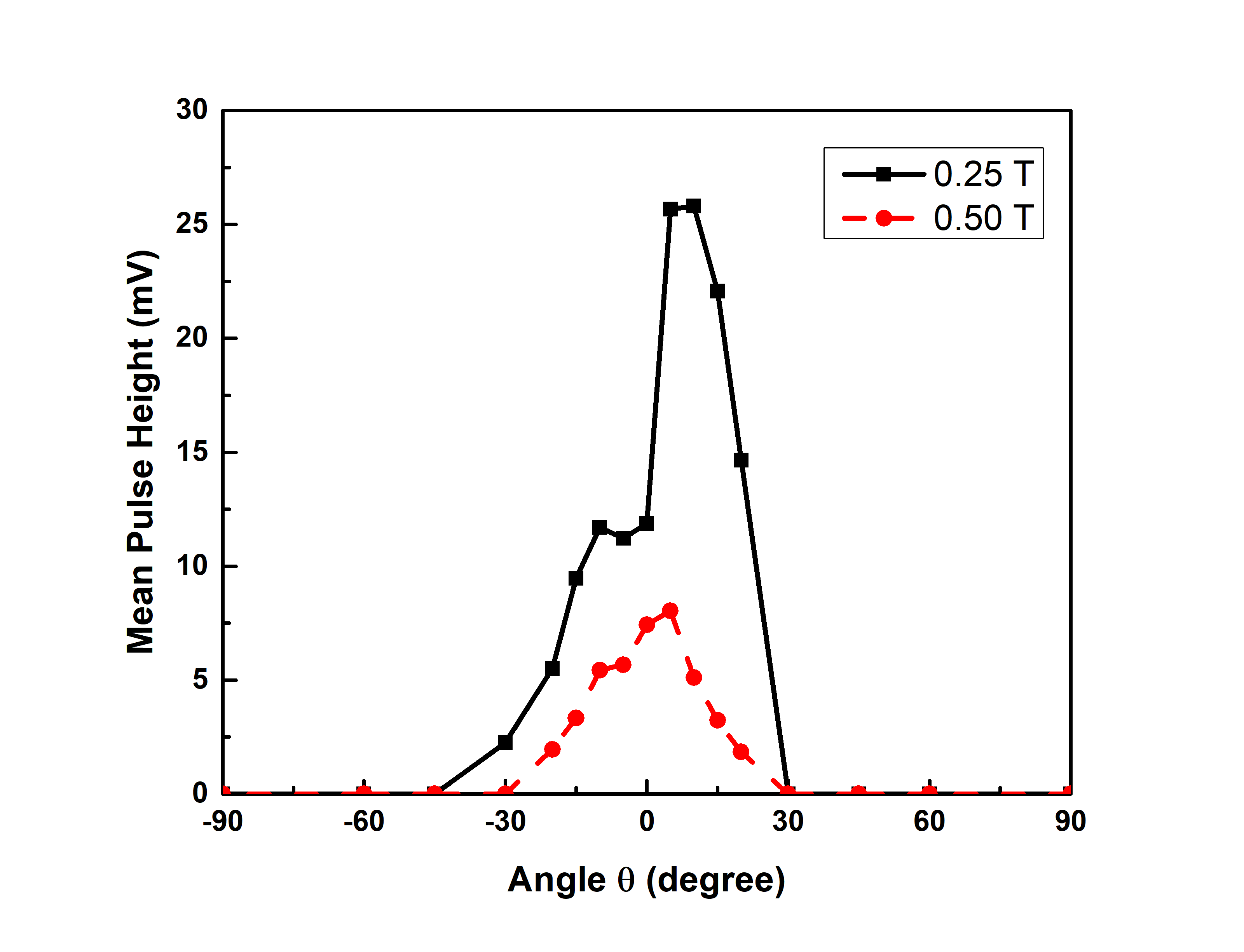
The angular dependence of the MCP photodetector was additionally studied by rotating the MCP photodetector along with angle relative to the magnetic field direction, as shown in Figure 5. We fixed the bias high voltage at 3000 V on the photodetector and rotated the photodetector from -90∘ to 90∘ for a full range of angle measurements. Figure 6 presents the response of the MCP photodetector, in terms of the mean pulse height, measured as a function of the rotation angle at two magnetic field strengths of 0.25 and 0.5 Tesla. For -30∘ or 30∘, any signal is hardly seperated from the noise level. Within -30∘ 30∘, there are two peaks at about = 8∘, which are due to the chevron configuration of two MCPs inside the photodetector. The detector’s response reaches a maximum when the pore of either MCP is well-aligned with the magnetic field direction. The intensities of the two peaks are different, which is due to the different effect from the top and bottom MCPs.
4.3 Design optimization of MCP photodetector
In the design of the EIC experiment, a 1.5 Tesla solenoid magnet will be used for tracking charged particles. The magnetic field tolerance requirement varies from detector to detector depending on their distances from the interaction point and the magnetic field direction. From our measurement, the 66 cm2 MCP photodetector has shown a good magnetic field tolerance of up to 0.8 Tesla, comparable to that of current commercially available MCP-PMTs ( 1.0 T) with similar pore size [17]. Here, we must emphasize that the current LAPPD design is not yet optimized for magnetic field tolerant applications. The distances between the photocathode, MCPs, and the anode are relatively large in the LAPPD design. For instance, the spacing between the photocathode and the top MCP of 2 mm and spacing between the bottom MCP and the anode of 3.2 mm [10]. To optimize for a magnetic field environment, these distances should be reduced to minimize the electron transit distance. Meanwhile, MCP photodetectors with smaller pore sizes have shown better magnetic field tolerance than those with larger pore sizes [17, 18, 19]. A redesign of the current LAPPD configuration with smaller pore sizes (e.g. 10 m or even 5 m) and reduced distances between the PMT elements should improve its magnetic field tolerance.
5 Conclusions
We have described the current design of 66 cm2 microchannel plate photodetectors with the next-generation MCPs functionalized through atomic layer deposition process. The rate capability and magnetic field tolerance of these photodetectors were tested using Fermilab’s 120 GeV proton beam and Argonne’s 4 Tesla magnetic field facility. The photodetectors exhibit stable performance for rates up to 75 kHz/cm2 and magnetic field tolerance for fields up to 0.8 Tesla. The magnetic field angle dependence was also measured, showing enhanced performance at 8∘ tilt angle due to the original MCP 8∘ bias angle. The magnetic field tolerance of these detectors could be further improved by using smaller pore size MCPs and redesigning the package with reduced distances between the photocathode, the MCPs, and the anode.
6 Acknowledgments
The authors would like to thank Frank Skrzecz (Engineer at ANL) for his mechanical engineering support; Joe Gregar (Scientific Glass Blower at ANL) for his talented work on glass parts; Peter Winter (Physicist at ANL) for his arrangement of the Argonne magnetic facility usage; the staff at Fermilab Test Beam Facility for their beamline support; and many people from the LAPPD collaboration for their advices and assistants. This material is based upon work supported by the U.S. Department of Energy, Office of Science, Office of High Energy Physics, Office of Nuclear Physics, under contract number DE-AC02-06CH11357. Work at Brookhaven National Laboratory was supported by the U. S. Department of Energy, Office of Science under contract No. DE-AC02-98-CH10886. This work was also partially supported by the EIC R&D funding from the Office of Nuclear Physics and Office of Science of the U.S. Department of Energy.
References
- [1] A. Accardi et al., Electron Ion Collider: The Next QCD Frontier, Eur. Phys. J. A 52 (2016) 268.
- [2] A. Aprahamian et al., Reaching for the horizon: The 2015 long range plan for nuclear science, 2015.
- [3] C.P. Wong et al., Modular focusing ring imaging Cherenkov detector for electron-ion collider experiments, Nucl. Instr. and Meth. A 871 (2017) 13.
- [4] A. Del Dotto et al., Design and R&D of RICH detectors for EIC experiments, Nucl. Instr. and Meth. A (2017).
- [5] G. Kalicy et al., High-performance DIRC detector for the future Electron Ion Collider experiment, JINST 11 (2016) C07015.
- [6] M. Minot et al., Pilot production & commercialization of LAPPDTM, Nucl. Instr. and Meth. A 787 (2015) 78.
- [7] B. Adams et al., A brief technical history of the Large-Area Picosecond Photodetector (LAPPD) Collaboration, 2016 arXiv:1603.01843.
- [8] J. Xie et al., Development of a small form-factor (6cm6 cm) picosecond photodetector as a path towards the commercialization of large area devices, in: Proceeding of “The Technology and Instrumentation in Particle Physics 2014”, PoS 2014.
- [9] J. Xie et al., Design and fabrication of prototype 66 cm2 microchannel plate photodetector with bialkali photocathode for fast timing applications, Nucl. Instr. and Meth. A 784 (2015) 242.
- [10] J. Wang et al., Development and testing of cost-effective, 6cm6cm MCP-based photodetectors for fast timing applications, Nucl. Instr. and Meth. A 804 (2015) 84.
- [11] J. Wang et al., Design improvement and bias voltage optimization of glass-body microchannel plate picosecond photodetector, IEEE Trans. Nucl. Sci. 64 (2017) 1871.
- [12] C. Craven et al., Recent advances in Large Area Micro-Channel Plates and LAPPDTM, Springer Proceedings in Physics (2017).
- [13] L. Xia et al., Systems and methods for forming microchannel plate (MCP) photodetector assemblies, U.S. Patent 9704900 B1, July 11, 2017.
- [14] DT5742 desktop digitizer http://www.caen.it
- [15] DRS chip developed at Paul Scherrer Institut, Switzerland https://www.psi.ch/drs
- [16] 4 Tesla Magnet Facility https://www.anl.gov/hep/group/4-tesla-magnet-facility
- [17] A. Lehmann et al., Performance studies of microchannel plate PMTs in high magnetic fields, Nucl. Instr. and Meth. A 595 (2008) 173.
- [18] A. Lehmann et al., Systematic studies of micro-channel plate PMTs, Nucl. Instr. and Meth. A 639 (2011) 144.
- [19] Y. Ilieva et al., MCP-PMT studies at the High-B test facility at Jefferson Lab, JINST 11 (2016) C03061.