Magnetic and electronic phase crossovers in graphene nanoflakes
Abstract
Manipulation of intrinsic magnetic and electronic structures of graphene nanoflakes is of technological importance. Here we carry out systematic study of the magnetic and electronic phases, and its manipulation in graphene nanoflakes employing first-principles calculation. We illustrate the intricate shape and size dependence on the magnetic and electronic properties, and further investigate the effects of carrier doping, which could be tuned by gate voltage. A transition from nonmagnetic to magnetic phase is observed at a critical flake size for the flakes without sublattice imbalance, which we identify to be originated from the armchair defect at the junctions of two sublattices on the edge. Electron, or hole doping simultaneously influences the magnetic and electronic structures, and triggers phase changes. Beyond a critical doping, crossover from antiferromagnetic to ferromagnetic phase is observed for the flakes without sublattice imbalance, while suppression of magnetism, and a possible crossover from magnetic to nonmagnetic phase is observed for flakes with sublattice imbalance. Simultaneous to magnetic phase changes, a semiconductor to (half) metal transition is observed, upon carrier doping.
I Introduction
Plausible applications in spin-based electronics and information processing (Rycerz et al., 2007; Yazyev, 2010; Roche and Valenzuela, 2014; Han et al., 2014; Bullard et al., 2015) have made unconventional magnetism in bonded 2D hexagonal network of C atoms in graphene a topic of recent discussion. Carbon based materials have unique advantages in this regard due to very weak spin-orbit and hyperfine coupling, (Trauzettel et al., 2007; Yazyev, 2008; Fischer et al., 2009) and high spin-wave stiffness. (Edwards and Katsnelson, 2006) Thus, magnetic carbon structures are expected to exhibit higher Curie temperature and spin correlation length, compared to conventional magnets. (Yazyev and Katsnelson, 2008) Further, the spin-transport in graphene could be manipulated easily by external perturbations such as electric fields. (Son et al., 2006a)
Magnetism in otherwise nonmagnetic graphene can be induced by the presence of point/extended defects (Yazyev and Helm, 2007; Palacios et al., 2008; Alexandre et al., 2012; Nair et al., 2013; Zhang et al., 2016) or through adatom adsorption. (Donati et al., 2013; González-Herrero et al., 2016) Alternatively, the non-trivial electron driven magnetism can be induced at the edges in finite graphene nanoflake (GNF) due to the localized edge states. (Nakada et al., 1996; Fujita et al., 1996; Klusek et al., 2000; Kobayashi et al., 2005, 2006) While the electron is localized at the carbon atoms on zigzag edge, no such localization is expected for armchair edge type. While graphene nanostructures have been fabricated, (Tombros et al., 2007; Han et al., 2007; Ponomarenko et al., 2008) the precise control over the edge type was limited until few years back. Only very recently using nanofabrication technique and scanning tunneling microscopy, nanoribbons with precise zigzag edge have been fabricated, and a robust long-range magnetic order has been observed at room temperature. (Magda et al., 2014) Further, semiconductor to metal transition accompanied by switching in the magnetic ordering between the edges has been predicted as a function of ribbon width. (Magda et al., 2014)
Graphene is a bipartite hexagonal lattice, which is formed by two interpenetrating triangular sublattices A and B. According to single-band Hubbard model, spins localized at the zigzag edge align in parallel if they belong to the same sublattice. In contrast, they become antiparallel if they belong to different sublattices. (Fernández-Rossier and Palacios, 2007) Thus, a long-range magnetic ordering is developed along the edge in finite graphene nanoflakes, and the total spin of the ground state follows Lieb’s theorem, . (Lieb, 1989) This picture has been confirmed through density functional theory based calculations in passivated flakes. (Fernández-Rossier and Palacios, 2007; Kabir and Saha-Dasgupta, 2014) Further, a magnetic phase transition has been predicted in hexagonal flakes due to carrier doping. (Kabir and Saha-Dasgupta, 2014) As the intrinsic magnetic ordering and corresponding ground state magnetization are related to sublattice identity of the edge atoms and total sublattice imbalance, an unified size and shape dependence of magnetism in nanoflakes is complex, and not yet fully explored.
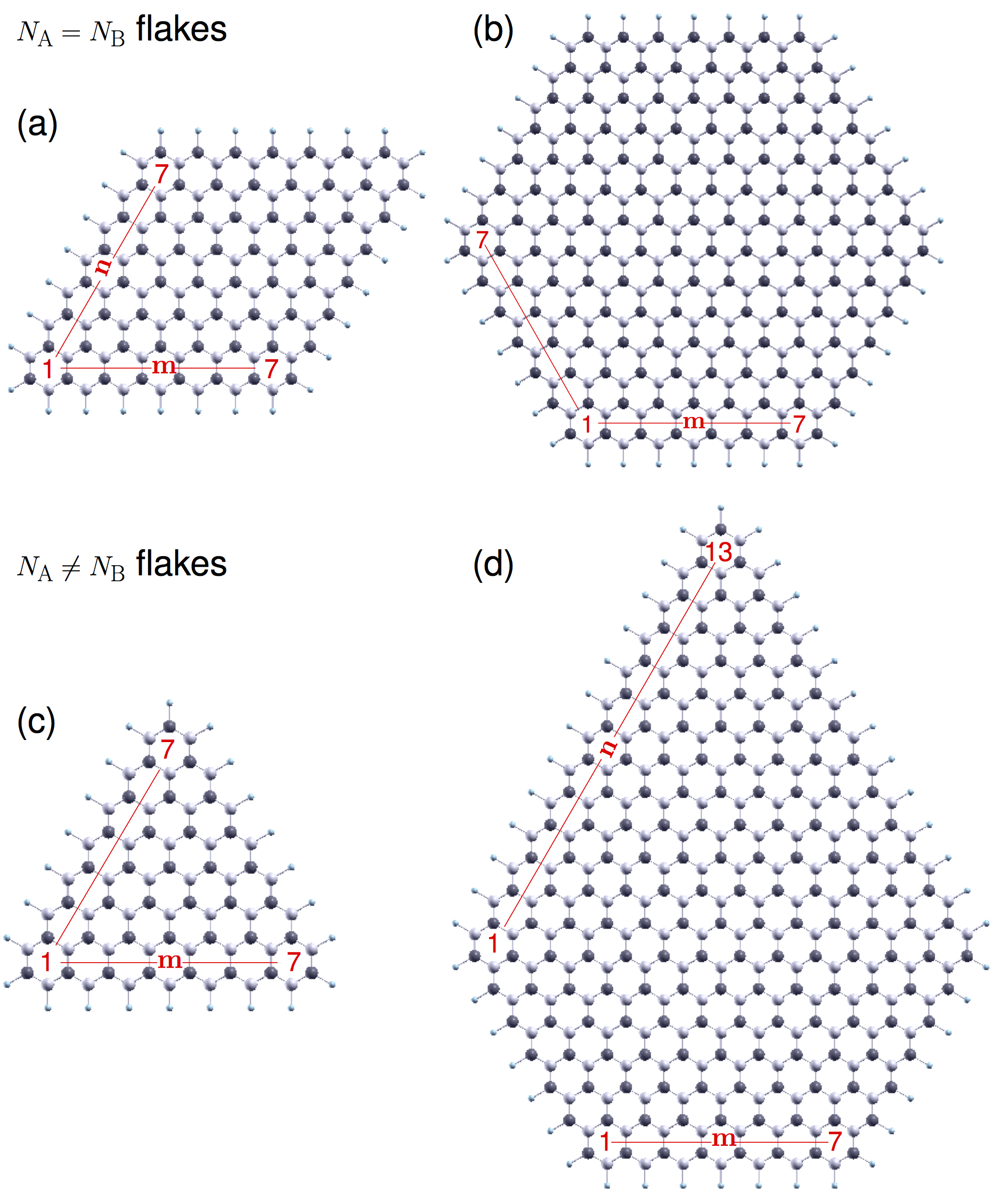
Here, we systematically address this intricate issue within first-principles calculations by considering graphene nanoflakes with various shapes and varied sizes. We have considered four shapes, rhombohedral, hexagonal, triangular and pentagonal. The nanoflakes with arbitrary shapes can be classified by sublattice imbalance; flakes with sublattice imbalance (such as triangular and pentagonal), and without imbalance (rhomohedral and hexagonal). In order to investigate the electrons only, the in-plane dangling bonds are passivated with single hydrogen atom. For the nanoflakes without any sublattice imbalance, the prediction of Lieb’s theorem may be satisfied either with a nonmagnetic solution or with a fully compensated intrinsic magnetic ordering. This may lead to a quantum phase transition with flake size. (Fernández-Rossier and Palacios, 2007) Indeed, for both rhombohedral (R) and hexagonal (H) shapes, we find that carbon atoms at the edge develop local moments beyond a critical size, and a crossover from nonmagnetic to compensated ferrimagnetic phase takes place. We characterize this with the armchair defect density at the edge, which is defined as the ratio of armchair bond (at the junction of A and B sublattices) with the number of zigzag bonds. In contrast, the flakes with sublattice imbalance, triangular (T) and pentagonal (P) flakes, are always found to be magnetic independent of their respective size.
Further, manipulation of intrinsic magnetic and corresponding electronic properties by external perturbations is key to spintronic applications. Thus, in addition to undoped flakes, we investigate the carrier doped flakes. Doping could be experimentally achieved by applied gate voltage. In this context, the half-filled Hubbard model in the Nagaoka limit, (Nagaoka, 1966) infinite bipartite lattice with essentially infinite Coulomb interaction, predicts a magnetic phase transition at the filling slightly away from the half-filling. However, the present cases of nanoflakes, neither of the Nagaoka limits are satisfied. Nonetheless, we observe the intrinsic magnetic structure is crucially entangled with the doped carrier density, and complex magnetic phase changes are predicted. Together with changes in magnetic phases, a semiconductor to (half) metal transition has been observed. With the current state of advancement in controlled experimental techniques, we hope that our theoretical observations will stimulate further experimental activity.
II Computational Details
Calculations were carried out within density functional theory (DFT) in the plane wave basis, as implemented in the Vienna Ab-initio Simulation Package (VASP). (Kresse and Hafner, 1993; Kresse and Furthmüller, 1996) The projector augmented wave pseudopotential was used with a plane-wave cutoff of 800 eV. (Blöchl, 1994) For the exchange-correlation functional, we used the Perdew-Burke-Ernzerhof (PBE) form of generalized gradient approximation (GGA). (Perdew et al., 1996) The reciprocal space integrations were carried out at the point. Within the periodic set-up of the calculations, flakes were placed in simple cubic supercells such that the periodic images are separated by at least 12 Å of vacuum space, which ensures the interaction between the images negligible. Nanoflakes were optimized until the forces on each atom became less than 5 10-3 eV/Å. Further, to understand the effect of electron-electron correlation beyond GGA, some of the calculations were repeated considering a Hubbard like on-site Coulomb interaction, (DFT+), within rotationally invariant approach. (Dudarev et al., 1998)
We considered regular T and H flakes with sizes =3, 5, 6, 8; and 3, 6, 7, 8, 9, 10, respectively, where is the number of hexagonal rings along their regular edge (Figure 1). The size of the R and P flakes are denoted by and , where and are lengths of dissimilar edges (Fig. 1). While 33, 35, 37, 44, 55, 77 were considered for the R flake, we considered 47, 59, 713, and 815 for the P flake.
III Results and discussion
We start our discussion with undoped GNFs to illustrate the intricate shape and size dependence of the intrinsic edge magnetism. We also investigate the effect of strong electron correlation on the magnetism. Having understood the intricate size, shape and correlation dependent magnetism in undoped GNFs, we discuss the effect of carrier doping on the magnetic and electronic structures.
III.1 Shape and size dependence of edge magnetism
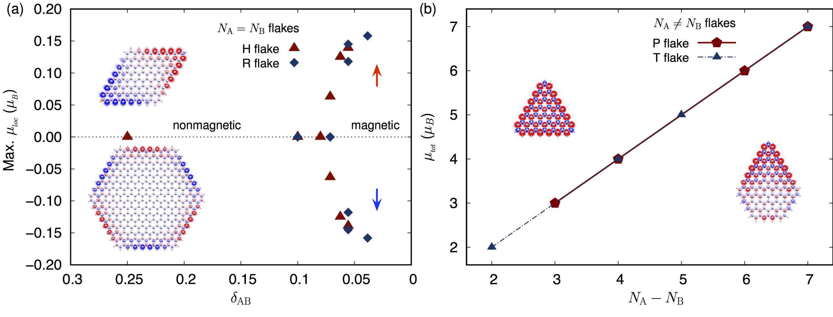
We find that the intrinsic magnetic structures of the GNFs are strongly dependent on both nanoflake shape and their size. The scenario for the flakes without any sublattice imbalance is particularly non-trivial, and a quantum phase transition is observed [Figure 2(a)]. For both R and H flakes, we find that only beyond a critical size, the carbon atoms at the edge develop a local moment, and a nonmagnetic to fully compensated ferrimagnetic phase change occurs at this critical size. For the magnetic R and H flakes, the intrinsic intra-edge coupling is found to be ferromagnetic as the atoms on a specific edge belong to particular sublattice. In contrast, antiferromagnetic coupling is observed between the edges, which belong to different sublattices [Figure 2(a)]. This picture is consistent with the predictions from the Hubbard model, and agrees well with the previous DFT calculations for H flakes. (Fernández-Rossier and Palacios, 2007; Kabir and Saha-Dasgupta, 2014) However, the origin of this size dependence has not been addressed previously. To characterize the observed magnetic phase transition with flake size, we define a unitless quantity , which relates to the armchair defects along the entire edge of the flake. There exists an armchair bond at the junctions of A and B sublattice [Figure 1 (a)], where electrons are delocalized, and thus is detrimental for magnetism. Thus, in the context of magnetism on zigzag edge, such armchair bonds act as defects. This is also evident from the magnetization density. The local moment along a particular edge has a distribution – zero at the armchair defect, and increases away from the armchair defects at the junctions of A and B sublattices [Figure 2(a)]. Thus, for H flakes, the carbon atoms at the middle of the edge has the maximum local moment. In comparison, for R flakes, progressively increases in moving towards the defect free corners, starting from the zero value at two armchair defects connecting A and B sublattices. We define the defect density as , where () is the number of armchair (total) bonds along the edge. Thus, decreases with increasing flake size. We find that beyond a critical flake size with corresponding 0.07, the edge atoms develop a moment, and the flakes become compensated ferrimagnet [Figure 2(a)]. It is important to note that with increasing flake size ( 0.07) the maximum local moment at the edge, increases, but keeping the net moment fixed at zero value, thus obeying the prediction of Lieb’s theorem.
In comparison, the size dependence of magnetism in T and P flakes having sublattice imbalance is far less complex. Independent of size, such flakes are found to be magnetic with the total ground state magnetization given by, , following Lieb’s theorem [Figure 2(b)]. Thus, with increase in size, the sublattice imbalance increases, leading to linear increase in . For T flakes, all the edge atoms belong to a particular sublattice, and thus the inter-edge coupling is ferromagnetic [Figure 2(b)]. The P flakes can be viewed as a fusion of T and H structures. While the edge atoms in the triangular region belong to the same sublattice, rest of the edges alternate between two sublattices [Figure 1(c) and Figure 1(d)]. The corresponding magnetic structure is thus commensurate with the ferromagnetic and antiferromagnetic inter-edge coupling between the same and different sublattices [insets in Figure 2(b)].
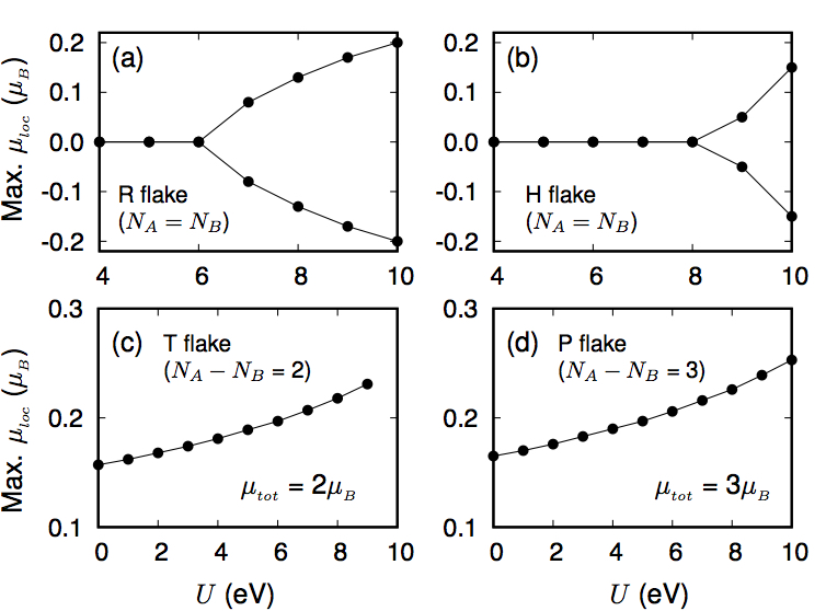
Next, we study the effect of strong electron correlation on the edge magnetism, as a strong Coulomb interaction has been argued for graphene nanostructures. (Wehling et al., 2011; Meng et al., 2010; Sorella and Tosatti, 1992; Paiva et al., 2005) The local Coulomb interaction is proposed to be as large as 9 eV, which is in between the values that predicts a spin-liquid phase (Meng et al., 2010) and a compensated antiferromagnetic phase. (Sorella and Tosatti, 1992; Paiva et al., 2005) Keeping this in mind, we have repeated our calculation by supplementing a Hubbard like on-site Coulomb interaction (0-10 eV) on the conventional PBE exchange-correlation. Only one representative size has been considered for each shape (Figure 3).
For the flakes without any lattice imbalance in the size range 0.07, the flakes are nonmagnetic, and with increase in on-site Coulomb interaction beyond a critical value the edge atoms develop a local moment [Figure 3 (a) and (b)]. Further, increases with , while the complete magnetic structure remains fully compensated ferrimagnet. This picture is similar to that with increasing flake size, which has been discussed in the previous section. Thus, we conclude that increasing size and increasing electron-electron correlation both help in enhancing the localized character of the edge states, thereby stabilizing magnetism. In contrast, in the presence of lattice imbalance, the flakes are always magnetic, and the increase in monotonically increases the local moment at the edge. However, the ground state magnetization is maintained at by compensated increase in A and B sublattice moments. This in turn confirms the validity of Lieb’s theorem irrespective of the level of theoretical approximation toward electron correlation. Due the absence of accurate estimate of for finite sized nanoflakes, and due to the fact that the flake size and affect the intrinsic magnetic structure in similar fashion, we ignore explicit incorporation of Coulomb interaction for rest of the paper. Rather, we will consider larger flakes with 0.07, where are flakes are already magnetic without explicit incorporation of electron correlation.
III.2 Effects of carried doping on edge magnetism
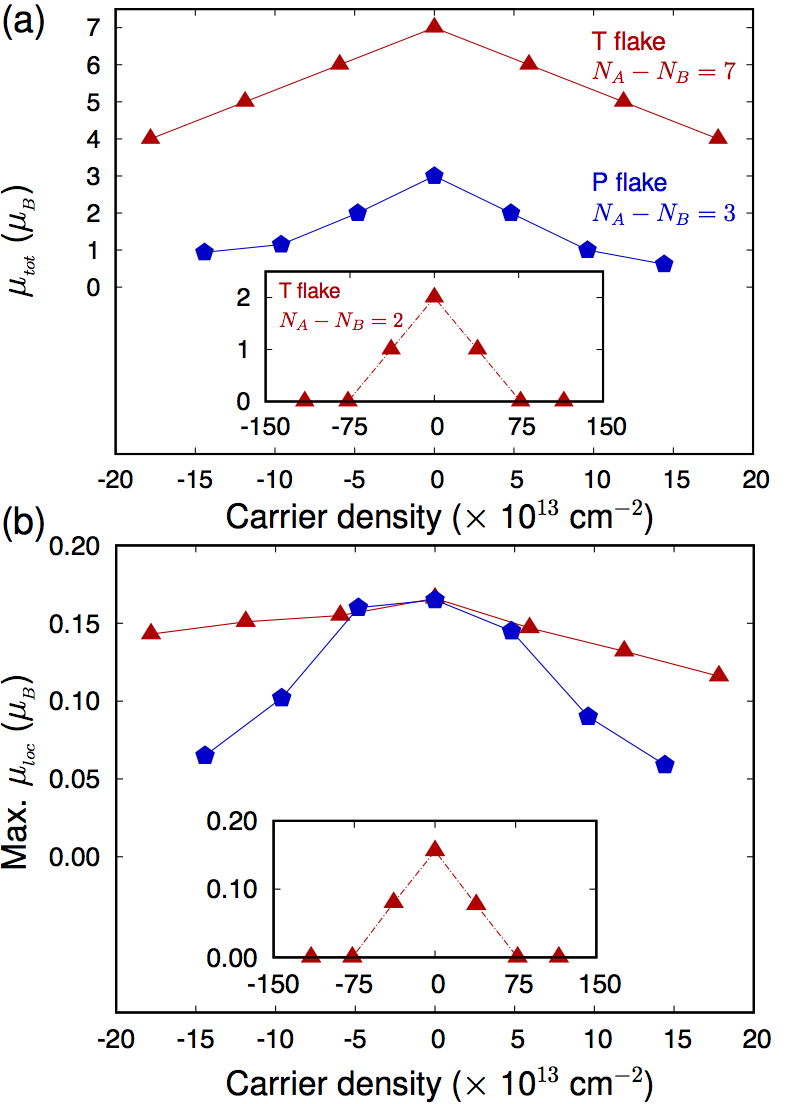
Next, we investigate the effect of carrier doping on the edge magnetism for nanoflakes with different shapes. The doped carrier density can be tuned experimentally, and possible manipulation of magnetic structure through gate voltage is fundamental to spintronic applications. We have considered both electron and hole doping with concentrations in the range 1013 1014 cm-2. Such high has been experimentally achieved. Nair et al. (2013); Dorgan et al. (2010); Ye et al. (2011) Similar to the undoped flakes, effect of carrier doping is found to be strongly shape dependent with sharp distinction in behavior of flakes with and without sublattice imbalance. Additionally, a magnetic phase transition is observed due to carrier doping, which is fundamentally interesting and could be of technological importance.
We first discuss the flakes with , which in undoped situation is always magnetic, independent of size [Figure 2(b)]. As discussed, the inter-edge coupling in T-flakes is ferromagnetic with ground state magnetization . Thus, the undoped T flakes with = 3, and 8 have 2 and 7 moment [Figure 4(a)]. Electron (hole) doping in these flakes decreases the value of to , where is the number of doped electron (hole). Thus, monotonically decreases with increasing carrier doping [Figure 4(a)], and flake becomes nonmagnetic beyond a critical . For larger =8 T flake, decreases to 4 due to 3 electron (hole) doping, which correspond a carrier doping of 1.79 1014 cm-2. The P flake magnetism upon carrier doping is found to be qualitatively similar to that of the T flakes.
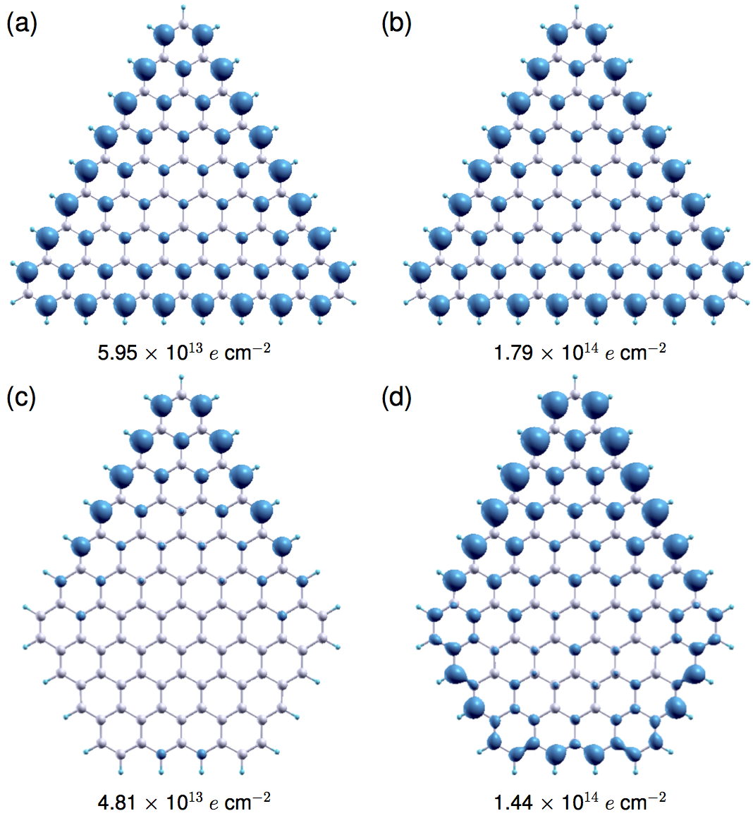
To understand the microscopic origin of such behavior in the flakes, we calculated for the edge atoms [Figure 4(b)], and investigated the partial charge density of the doped electron (hole), shown for =8 T flake and 47 P flakes [Figure 5(a) – (d)]. We find that doped carrier is distributed mainly on the edge atoms, and entirely on A sublattice. Further, they occupy the minority channel, which leads to a decrease in calculated with carrier doping [Figure 4(b)]. Concurrently, decreases by from the neutral ground state. However, such a picture breaks down at higher doping for the P flakes, and the corresponding ground state spin is higher than expected as discussed before. At higher doping limit beyond 9.62 1013 cm-2, although the carrier is predominantly distributed over the A sublattice, a fraction populates the minority channel of the B sublattice. Thus, the decrease in becomes slower than expected [Figure 4(a)]. Interestingly for all flakes, though the calculated and decreases upon carrier doping, the intrinsic intra-edge and inter-edge magnetic coupling remain same as for the undoped flakes.
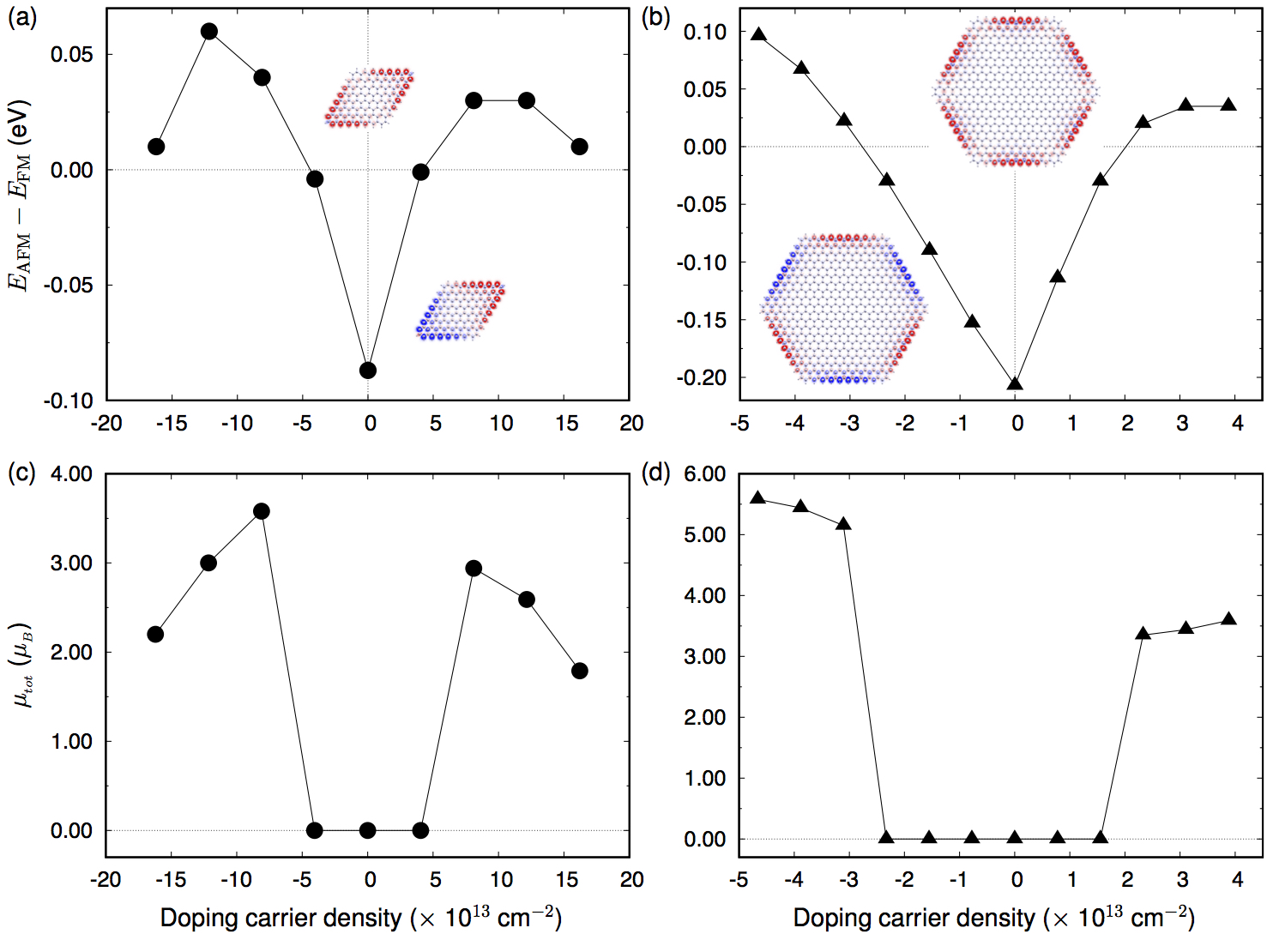
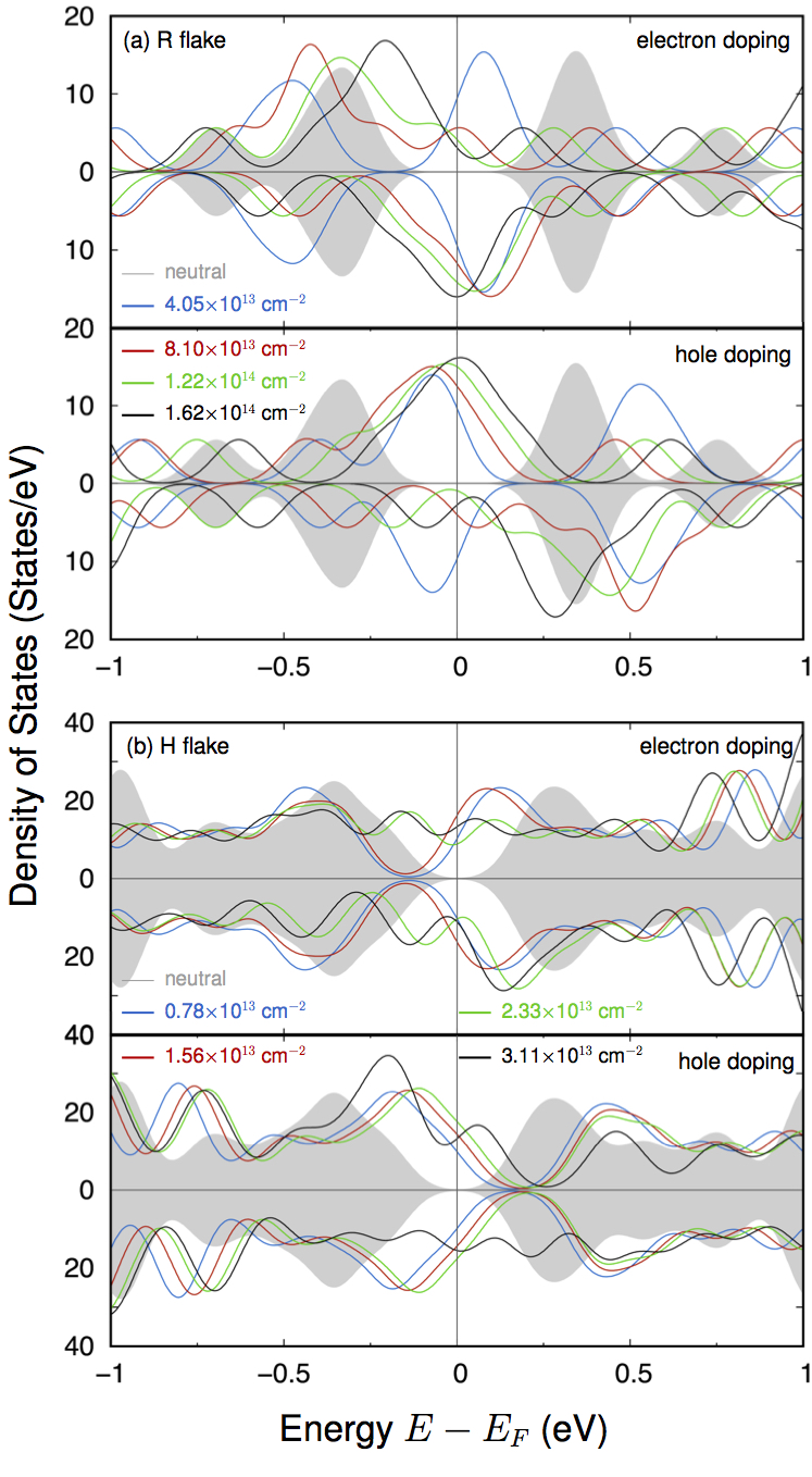
In contrast, carrier doping affects the magnetism in flakes in a non-trivial fashion. As we have discussed earlier that a nonmagnetic to compensated ferrimagnetic phase transition occurs at a critical size characterized by 0.07 [Figure 2(a)]. Here, we consider R and H flakes with 0.07, which is magnetic in their neutral state, and investigate the effect of carrier doping. Interestingly, we find a magnetic phase transition upon carrier doping beyond a critical [Figure 6(a) and (b)]. The inter-edge coupling becomes ferromagnetic with non-zero [Figure 6(c) and (d)]. Thus, the impact of carrier doping is substantially different in these flakes than for the flakes with sublattice imbalance. While, carrier doping affects , and thus in flakes without affecting the nature of long-range order, a phase transition is observed for flakes. Further, electron-hole asymmetry is observed in terms of stabilization of a particular magnetic phase [Figure 6 (a) and (b)], although the phase transition is induced by both electron and hole doping. In case of R flakes, we notice a plausible re-entrance to compensated ferrimagnetic phase as the energy difference decreases at large .
III.3 Effects of carried doping on electronic structure
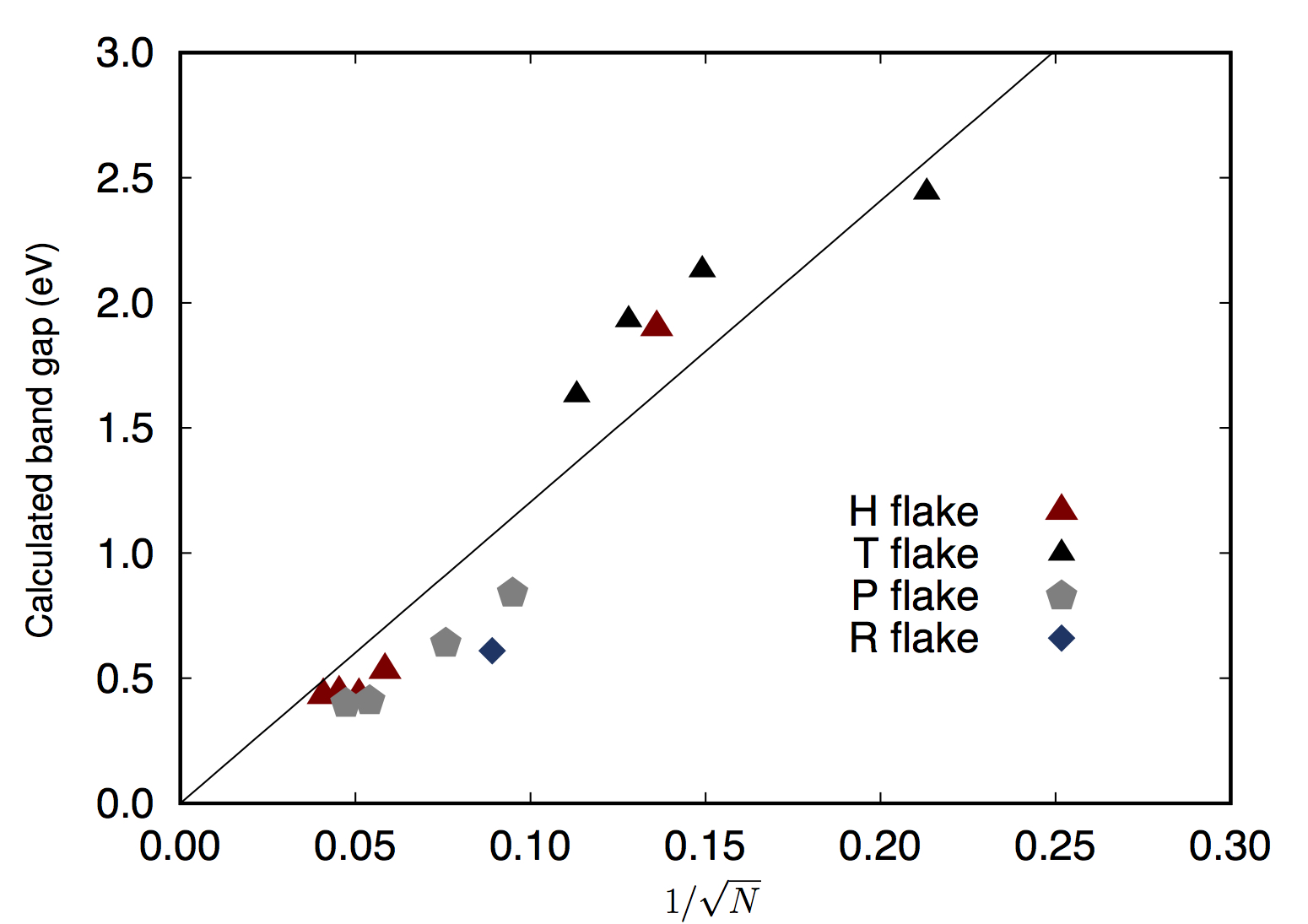
Although bulk graphene is a semimetal with zero density of states at the Dirac points, the electronic structure of graphene quantum dots and ribbons depend sensitively on the crystallographic orientation of their edges. (Son et al., 2006a; Han et al., 2007; Ponomarenko et al., 2008; Barone et al., 2006; Son et al., 2006b; Li et al., 2008; Singh et al., 2014; Hu et al., 2014) The neutral flakes are found to be semiconducting and the calculated gaps decrease with increasing flake size, which we characterize by the total number of atoms in the flake (Figure 7). Although, the gap should go to zero at infinite size, the asymptotic interpolation might be complex, (Singh et al., 2014; Hu et al., 2014) due to intricate dependence on the flake shape, and corresponding magnetism. However, regardless the shape, the neutral flakes are found to be semiconducting in the studied size range (Figure 7). Thus, it would be interesting to investigate the effect of carrier doping on the semiconducting nature of these flakes.
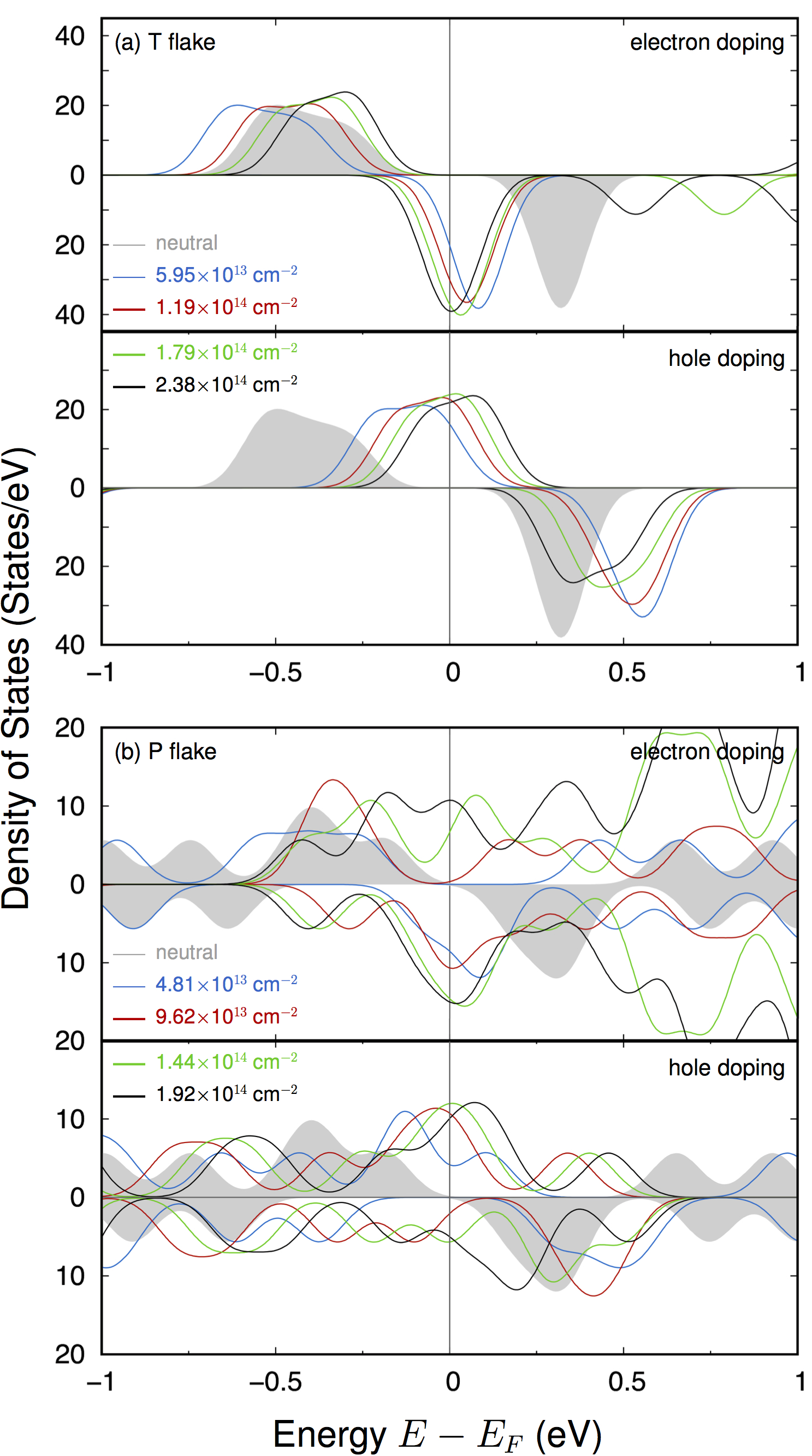
We observe an electronic phase transition in these flakes, and semiconducor to (half) metal transition is observed due to carrier doping. We first investigate the flakes in detail, where we particularly consider the =8 T flake and 47 P flakes. The neutral =8 T flake is a semiconductor with 1.29 (1.27) eV gap in the majority (minority) channel. Careful investigation of the density of states (DOS) indicate that the highest occupied majority states lie 0.10 eV below the Fermi level , whereas the unoccupied minority states lie 0.11 eV above . Single electron (hole) doping with corresponding =5.951013 cm-2 alters the electronic structure and transform the flake into half-metallic [Figure 8 (a)]. The flake remains half-metallic upon further doping.
The otherwise unoccupied minority channel gets populated by electron doping [Figure 8 (a)], and thus the minority channel becomes conducting. In contrast, for hole doping, electrons are removed from the majority channel, and thus moves lower in energy. This leads to a gap closing in the majority channel [Figure 8 (a)]. While increase in electron doping monotonically increases the DOS at , for hole doping the is continuously pushed toward lower energy. Therefore, the overall qualitative picture remains similar with the increase in , and the solution remains half-metallic [Figure 8 (a)] at all . Thus, T flakes will manifest completely spin-polarized transport under applied gate voltage. Further, it would be possible to control conduction in a particular channel (majority or minority) by controlling the polarity of the gate voltage (electron or hole doping). This would be significant importance in the context of spin-based electronics.
The carrier induced evolution of electronic structure in P flakes is qualitatively different. A semiconductor to half-metal to metal transition is observed with increasing carrier density. The neutral 47 P flake is semiconducting with 0.55 (0.51) eV gap in the majority (minority) channel. While the highest occupied states appear 0.05 eV below the , the lowest unoccupied states 0.05 above the . For electron doping with 9.62 1013 cm-2, the doped electron populates the minority channel only, and the flake becomes half-metallic [Figure 8 (b)]. Further increase in electron density populates both majority and minority channels simultaneously, and a metallic solution emerges for 1.44 1014 cm-2. In contrast, for hole doping, electrons are removed from the majority channel only for 9.62 1013 cm-2. As the moves lower in energy, a half-metallic solution emerges. Further increase in hole doping depletes electrons from both the channels, and the ground state becomes metallic. This picture also explains the emergence of non-integer for the corresponding ground state, and also illustrates the slow decrease in for the metallic P flakes, at high carrier doping.
We next discuss the carrier dependent electronic structure for the flakes without sublattice imbalance, . Here, we consider a 77 R flake, and a =10 H flake, which show fully compensated ferrimagnetic structure. These flakes have 240 and 200 meV semiconducting gaps, respectively, in their neutral states. Independent of flake shape, a semiconductor to metal transition is observed [Figure 9(a) and (b)], without any appearance of half-metallic solution. As the inter-edge coupling is antiferromagnetic in these flakes, the doped electron equally populates the majority and minority channels. Thus, gaps in both the channels disappear and the flakes become metallic. Similarly, the electrons are depleted from both the channels due to hole doping. Thus the continuously shifts to a lower energy and the solutions become metallic. Similar semiconductor to metal transition has been experimentally observed in graphene nanoribbons. (Magda et al., 2014)
IV Summary
Using first-principles calculations, we carried out a systematic study of the magnetic and electronic structures of graphene nanoflakes with different shapes and sizes. Further, the effect of carrier doping was investigated, which could be accessed experimentally by gate voltage. The presence or absence of sublattice imbalance plays a crucial role in magnetism. For flakes without any sublattice imbalance, a nonmagnetic to magnetic phase transition is observed with increasing flake size, which is characterized by the armchair defect concentration along the edge. We find that beyond a critical flake size 0.13, the carbon atoms at the edge develop local moments and the fake becomes magnetic. In contrast, the flakes with sublattice imbalance are always found to be magnetic. Further, for the neutral flakes with any shape, the edge moments from the same sublattice couple ferromagnetically, while antiferromagnetic coupling is observed between the moments from a different sublattice. This is in agreement with the mean-field solution of the Hubbard model, and in all cases the ground state magnetization follow Lieb’s prediction, .
We find that the magnetic phase transition is induced by carrier doping. For flakes, beyond a critical doping antiferromagnetic to ferromagnetic phase transition is observed. In contrast, carrier doping suppresses the magnetism in flakes. In these flakes, the local moments at the edge, and thus monotonically decreases with increasing doping. This indicates that at very high doping density the flakes may become nonmagnetic. Further, a simultaneous electronic phase transition is observed in response to carrier doping. In this regard, the cases with sublattice imbalance is found to be more interesting. A semiconductor to half-metal, and a semiconductor to half-metal to metal transition is observed in T and P flakes, respectively. In particular, the half-metallic solution is interesting, and may lead to fully polarized transport. In contrast, for the flakes, a semiconductor to metal transition take place without an appearance of half-metallic solution. Finally, we propose that nano-lithographic technique coupled with scanning tunneling microscopy will be able to verify our theoretical prediction of complex size and shape-dependent magnetic and electronic phase transitions in graphene flakes, which may lead to electronic and spintronic applications.
Acknowledgements.
Some of the reported calculations have been done using the supercomputing facilities at the Centre for Development of Advanced Computing, Pune; Inter University Accelerator Centre, Delhi; and at the Center for Computational Materials Science, Institute of Materials Research, Tohoku University. M. K. acknowledges the funding from the Department of Science and Technology, Government of India under Ramanujan Fellowship, and Nano Mission project SR/NM/TP-13/2016(G).References
- Rycerz et al. (2007) A. Rycerz, J. Tworzydlo, and C. W. J. Beenakker, Nat. Phys. 3, 172 (2007).
- Yazyev (2010) O. V. Yazyev, Rep. Prog. Phys. 73, 056501 (2010).
- Roche and Valenzuela (2014) S. Roche and S. O. Valenzuela, J. Phys. D 47, 094011 (2014).
- Han et al. (2014) W. Han, R. K. Kawakami, M. Gmitra, and J. Fabian, Nat. Nano. 9, 794 (2014).
- Bullard et al. (2015) Z. Bullard, E. C. Girão, J. R. Owens, W. A. Shelton, and V. Meunier, Sci. Rep. 5, 7634 (2015).
- Trauzettel et al. (2007) B. Trauzettel, D. V. Bulaev, D. Loss, and G. Burkard, Nat. Phys. 3, 192 (2007).
- Yazyev (2008) O. V. Yazyev, Nano Lett. 8, 1011 (2008).
- Fischer et al. (2009) J. Fischer, B. Trauzettel, and D. Loss, Phys. Rev. B 80, 155401 (2009).
- Edwards and Katsnelson (2006) D. M. Edwards and M. I. Katsnelson, Journal of Physics: Condensed Matter 18, 7209 (2006).
- Yazyev and Katsnelson (2008) O. V. Yazyev and M. I. Katsnelson, Phys. Rev. Lett. 100, 047209 (2008).
- Son et al. (2006a) Y.-W. Son, M. L. Cohen, and S. G. Louie, Nature 444, 347 (2006a).
- Yazyev and Helm (2007) O. V. Yazyev and L. Helm, Phys. Rev. B 75, 125408 (2007).
- Palacios et al. (2008) J. J. Palacios, J. Fernández-Rossier, and L. Brey, Phys. Rev. B 77, 195428 (2008).
- Alexandre et al. (2012) S. S. Alexandre, A. D. Lúcio, A. H. C. Neto, and R. W. Nunes, Nano Lett. 12, 5097 (2012).
- Nair et al. (2013) R. R. Nair, I. L. Tsai, M. Sepioni, O. Lehtinen, J. Keinonen, A. V. Krasheninnikov, A. H. Castro Neto, M. I. Katsnelson, A. K. Geim, and I. V. Grigorieva, Nature Commun. 4, 2010 (2013).
- Zhang et al. (2016) Y. Zhang, S.-Y. Li, H. Huang, W.-T. Li, J.-B. Qiao, W.-X. Wang, L.-J. Yin, K.-K. Bai, W. Duan, and L. He, Phys. Rev. Lett. 117, 166801 (2016).
- Donati et al. (2013) F. Donati, Q. Dubout, G. Autès, F. Patthey, F. Calleja, P. Gambardella, O. V. Yazyev, and H. Brune, Phys. Rev. Lett. 111, 236801 (2013).
- González-Herrero et al. (2016) H. González-Herrero, J. M. Gómez-Rodríguez, P. Mallet, M. Moaied, J. J. Palacios, C. Salgado, M. M. Ugeda, J.-Y. Veuillen, F. Yndurain, and I. Brihuega, Science 352, 437 (2016).
- Nakada et al. (1996) K. Nakada, M. Fujita, G. Dresselhaus, and M. S. Dresselhaus, Phys. Rev. B 54, 17954 (1996).
- Fujita et al. (1996) M. Fujita, K. Wakabayashi, K. Nakada, and K. Kusakabe, J. Phys. Soc. Japan 65, 1920 (1996).
- Klusek et al. (2000) Z. Klusek, Z. Waqar, E. Denisov, T. Kompaniets, I. Makarenko, A. Titkov, and A. Bhatti, Appl. Surf. Sci. 161, 508 (2000).
- Kobayashi et al. (2005) Y. Kobayashi, K.-i. Fukui, T. Enoki, K. Kusakabe, and Y. Kaburagi, Phys. Rev. B 71, 193406 (2005).
- Kobayashi et al. (2006) Y. Kobayashi, K.-i. Fukui, T. Enoki, and K. Kusakabe, Phys. Rev. B 73, 125415 (2006).
- Tombros et al. (2007) N. Tombros, C. Jozsa, M. Popinciuc, H. T. Jonkman, and B. J. van Wees, Nature 448, 571 (2007).
- Han et al. (2007) M. Y. Han, B. Özyilmaz, Y. Zhang, and P. Kim, Phys. Rev. Lett. 98, 206805 (2007).
- Ponomarenko et al. (2008) L. A. Ponomarenko, F. Schedin, M. I. Katsnelson, R. Yang, E. W. Hill, K. S. Novoselov, and A. K. Geim, Science 320, 356 (2008).
- Magda et al. (2014) G. Z. Magda, X. Jin, I. Hagymasi, P. Vancso, Z. Osvath, P. Nemes-Incze, C. Hwang, L. P. Biro, and L. Tapaszto, Nature 514, 608 (2014).
- Fernández-Rossier and Palacios (2007) J. Fernández-Rossier and J. J. Palacios, Phys. Rev. Lett. 99, 177204 (2007).
- Lieb (1989) E. H. Lieb, Phys. Rev. Lett. 62, 1201 (1989).
- Kabir and Saha-Dasgupta (2014) M. Kabir and T. Saha-Dasgupta, Phys. Rev. B 90, 035403 (2014).
- Nagaoka (1966) Y. Nagaoka, Phys. Rev. 147, 392 (1966).
- Kresse and Hafner (1993) G. Kresse and J. Hafner, Phys. Rev. B 47, 558 (1993).
- Kresse and Furthmüller (1996) G. Kresse and J. Furthmüller, Phys. Rev. B 54, 11169 (1996).
- Blöchl (1994) P. E. Blöchl, Phys. Rev. B 50, 17953 (1994).
- Perdew et al. (1996) J. P. Perdew, K. Burke, and M. Ernzerhof, Phys. Rev. Lett. 77, 3865 (1996).
- Dudarev et al. (1998) S. L. Dudarev, G. A. Botton, S. Y. Savrasov, C. J. Humphreys, and A. P. Sutton, Phys. Rev. B 57, 1505 (1998).
- Wehling et al. (2011) T. O. Wehling, E. Şaşıoğlu, C. Friedrich, A. I. Lichtenstein, M. I. Katsnelson, and S. Blügel, Phys. Rev. Lett. 106, 236805 (2011).
- Meng et al. (2010) Z. Y. Meng, T. C. Lang, S. Wessel, F. F. Assaad, and A. Muramatsu, Nature 464, 847 (2010).
- Sorella and Tosatti (1992) S. Sorella and E. Tosatti, Europhys. Lett. 19, 699 (1992).
- Paiva et al. (2005) T. Paiva, R. T. Scalettar, W. Zheng, R. R. P. Singh, and J. Oitmaa, Phys. Rev. B 72, 085123 (2005).
- Dorgan et al. (2010) V. E. Dorgan, M.-H. Bae, and E. Pop, Appl. Phys. Lett. 97, 082112 (2010).
- Ye et al. (2011) J. Ye, M. F. Craciun, M. Koshino, S. Russo, S. Inoue, H. Yuan, H. Shimotani, A. F. Morpurgo, and Y. Iwasa, Proc. Natl. Acad. Sci. USA 108, 13002 (2011).
- Barone et al. (2006) V. Barone, O. Hod, and G. E. Scuseria, Nano Lett. 6, 2748 (2006).
- Son et al. (2006b) Y.-W. Son, M. L. Cohen, and S. G. Louie, Phys. Rev. Lett. 97, 216803 (2006b).
- Li et al. (2008) X. Li, X. Wang, L. Zhang, S. Lee, and H. Dai, Science 319, 1229 (2008).
- Singh et al. (2014) S. K. Singh, M. Neek-Amal, and F. M. Peeters, J. Chem. Phys. 140, 074304 (2014).
- Hu et al. (2014) W. Hu, L. Lin, C. Yang, and J. Yang, J. Chem. Phys. 141, 214704 (2014).