Self-assembled metallic nanoparticle template — a new approach of surface nanostructuring at nanometer scale111This work was initiated few years ago and the authors had the great opportunities to discuss the results with Jean-Pierre Badiali. We are extremely grateful for that.
Abstract
In the present work, the formation of silver and copper nanostructures on highly oriented pyrolytic graphite (HOPG) modified with self-assembled gold nanoparticles (Au NPs) is demonstrated. Surface patterning with nanometer resolution was achieved. Different methods such as field emission scanning electron microscopy (FEGSEM), energy dispersive spectrometry (EDS) and X-ray photoelectron spectroscopy (XPS) were used to illustrate a selective deposition of silver and copper on Au NPs. The mechanism of silver and copper ions reduction on Au NP with -dodecanethiol coating is discussed.
Key words: nanopatterning, electrodeposition, gold nanoparticles, silver and copper deposits
PACS: 81.07.-b, 81.16.-c, 81.16.Rf, 81.15.Pq, 81.16.Dn
Abstract
В данiй роботi продемонстровано наноструктури срiбла i мiдi на високо орiєнтованому пiролiтичному графiтi (HOPG), модифiкованому самозгромадженими золотими наночастинками (Au NPs). Отримано формування рисунку на поверхнi з нанометровою роздiльною здатнiстю. Рiзнi методи, такi як автоелектронний скануючий мiкроскоп (FEGSEM), енергетично розсiювальний спектрометр (EDS) i X-променева фотоелектронна спектроскопiя, були використанi для того, щоб проiлюструвати селективне осадження срiбла i мiдi на Au NP. Обговорено механiзм меншання iонiв срiбла i мiдi на Au NP з покриттям n-додеканетiолом.
Ключовi слова: наноструктурування, електроосадження, золотi наночастинки, осади золота i мiдi
1 Introduction
Most recently, structured materials at the nanometre scale have attracted even more attention due to the attempts to develop nanotechnological devices in many fields such as information storage [1, 2], optoelectronics [3, 4], electrochemical sensing [5, 6], solar cells [7, 8], catalysis [9], etc. The spatial periodicity of the nanostructure is expected to play a crucial role in the determination of the device properties [10, 11, 12]. For this purpose, different strategies have been developed to pattern the surface at the nanometer scale with high resolution and accuracy. Among the strategies used, a self-assembled colloidal particle template with well-defined geometry [13, 14, 15] provides a simple and easy strategy to achieve nanostructured materials. This strategy is a ‘‘bottom up’’ approach which allows the use of a wide choice of components to enable access to diverse physical properties with accurate control.
For the surface nanostructuring, two approaches were used: direct deposition [16] and deposition on a modified substrate (template) [17]. Using a scanning tunneling microscope, localized electrodeposition of metal has been successfully achieved, but it is difficult to control the location of a metal deposit with high lateral precision [18]. However, a direct deposition patterning usually has the disadvantage of achieving a disordered pattern due to the preferential nucleation at surface defects such as crystalline defects and step edges [19, 20, 21, 22, 23, 24]. To overcome this problem, a templated surface with patterns acting as preferential nucleation sites is proposed. Among the techniques used for metal deposition, the electrochemical deposition became a versatile tool for surface structuring and modification at nanometer scale [19, 20, 21, 22, 23, 24, 25]. It is relatively cheap and highly selective in that the new phase is deposited on the desired location.
The properties of electrodeposits depend on the surface properties, such as its topographical and chemical roughnesses [26]. Dos Santos Carlo et al. show that silver coated nanocavities act as preferred sites for silver electrodeposition [26]. Another strategy for surface patterning is the creation of preferential nucleation sites for electrodeposition at a very low scale using a mask made of self-assembled molecular film [27, 28] or colloidal particles [29, 30, 31]. Most of the published work deals with the use of the particles as a mask, and only a few works concern their use as nucleation sites. A recently published method that is particularly relevant to this work showed vertical ZnO nanowire arrays growth on an Au NPs-modified ZnO seed layer by using the vapor-liquid-solid (VLS) deposition method [29]. Metallic particles act as templates, through appropriate curvatures and/or their metallic nature, to create preferential deposition sites on the surface.
In this work, the advantage of using a self-assembled Au NPs template to create preferential sites for metal electrodeposition is reported. For a short electrodeposition time, there is illustrated a capability of self-assembled Au NPs template to control metal electrodeposition at nanometer scale. Ordered nanostructures with nanometer resolution were prepared. It is shown that this patterning method allows to achieve a lower resolution of about 2 nm.
2 Experimental details
Silver and copper electrodeposition is performed using a three electrode electrochemical configuration. The reference and counter electrodes were, respectively, Ag/AgCl and a platinum sheet. A clean (0001) highly oriented pyrolytic graphite (HOPG) surface was used as a working electrode and was prepared through a cleaving process. The modified HOPG electrode is prepared by depositing a droplet of Au NPs solution on the HOPG surface. Silver is deposited from an aqueous solution of M AgNO3 and 1 M HClO4 as a supporting electrolyte. Cu was deposited from the aqueous solution of M CuSO4 and 1 M H2SO4 as a supporting electrolyte. These solutions are deaerated by purified nitrogen during 2 h before use. AgNO3, HClO4 are obtained from Fluka. CuSOO and H2SO4 are purchased from Merck. All the chemicals used are of analytical grade and are used without further purification. The electrolytes are prepared with water purified by Milli Q system (Millipore, electric resistivity 18.2 M).
The 4 nm Au and silver (Ag) NPs are synthesized using the Stucky method [32]. After the synthesis, Au and Ag NPs are coated with -dodecanethiol and present a narrow size distribution (6%). By depositing a droplet of Au or Ag NPs solution on HOPG electrode, a 2D assembly of these nanoparticles in a hexagonal structure is obtained.
Electrochemical measurements (chronoamperometry) are performed with a Voltalab PGZ301 potentiostat and are carried out at room temperature. The chronoamperometry is obtained at constant potentials of V (vs. SCE) and V (vs. Ag/AgCl), respectively, for copper and silver electrodeposition over 10 s.
The morphologies of silver and copper electrodeposits and Au NPs film are investigated, using a high-resolution Ultra 55 Zeiss field emission gun scanning electron microscope (FEGSEM) and a transmission electron microscope (JOEL 100CX) operated at 100 kV.
Chemical compositions of the deposits are identified in FEGSEM using a PGT spirit energy dispersive spectrometry system (EDS). Additionally, for chemical composition determination, we used X-ray photoelectron spectroscopy (XPS) realized with a thermo VG Scientific ESCALAB 250 system fitted with a microfocused, monochromatic AL K X-ray source ( eV, spot size 650 µm, W).
3 Results and discussion
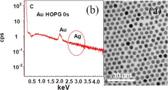
The HOPG electrode was modified by drop coating using a droplet of Au NPs solution on the surface, which then self-organizes in a hexagonal structure [figure 1 (a)]. It has been shown that the nanoparticle size, shape and surfactant shell are the main parameters determining the structure formed in the self-assembly process [33]. Thus, for ordered closely packed nanoparticles arrays with long range, both a narrow size distribution and an adequate capping ligand surface coverage are required. In fact, the passivating ligand lubricates the interface between the nanoparticles and the HOPG surface enhancing the nanoparticles diffusion to form a well arrangement in long range. Moreover, this shell should be highly repulsive at a close range but thin enough to maintain a short interparticle separation, a crucial factor in the physical properties (electronic and optical) of metal nanoparticles assembly. In our case, the optimum conditions for the formation of a close 2D hexagonal array with a high degree and long range ordering observing the arguments mentioned above are obtained using -dodecanethiol molecules. The long range ordering is crucial for a surface nanostructuring approach proposed in the present work.
The structural parameters of the organized array of -dodecanethiol-capped Au NPs depend on the configuration of the -dodecanethiol alkyl chain. This surfactant serves not only as a protective layer for the nanoparticles, preventing the coalescence and the consequent collapse of the structure, but also fixes the interparticle distance [13]. The distance between two nanoparticles obtained from TEM patterns is found to be between 1.8 and 2 nm. This similarity between the average interparticle distance and the length of alkyl chains suggests the intercalation or interpenetration of individual chains or domains of chains [34].
FEGSEM images shown in figure 2 (a) and 2 (c) are the obtained results of Ag and Cu electrodeposition achieved with an Au NPs modified HOPG electrode. It should be noted that Cu and Ag deposits have taken place on Au NPs and appear as bright spots. Furthermore, homogeneous distribution of Cu and Ag deposits on the surface can be observed.
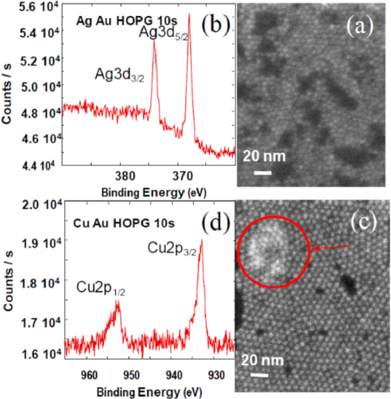
The EDS and XPS analyses have been performed to determine the chemical composition of the electrodeposited nanoparticles. Figure 1 (b) represents the EDS spectra of Au NPs-modified HOPG electrode before metal electrodeposition (Ag and Cu). It should be noted that only Au signal is observed, corresponding to Au NPs modified HOPG substrate. After 10 s copper and silver electrodeposition, this should be noted by a high resolution XPS spectrum, the appearance of different peaks corresponding to Ag3 and Cu2 core level [figure 2 (b) and 2 (d)] appeared.
For a further illustration of the patterning effect of Au NPs, FEGSEM patterns are compared to TEM image of Au NP-modified HOPG electrodes before metal electrodeposition. It can be seen that after 10 s electrodeposition, the hexagonal pattern formed by Au NPs is still preserved and the Ag and Cu deposits are reproducing this initial structure [figure 2 (a) and 2 (c)]. These results exclude any silver or copper electrodeposition between the Au NPs, otherwise coalesced nanoparticles should be observed. In the indicated region of figure 2 (c) there can be observed Cu nanoparticles bigger than Au NPs diameter (4 nm). It is also seen that some Cu nanoparticles start to coalesce with the disappearance of the hexagonal structure of Au NPs assembly.
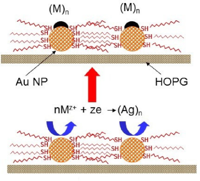
These results clearly show that using an electrodeposition process and Au NPs template a surface patterning with a resolution, deposit-to-deposit distance, of around 2 nm is achieved. This resolution is limited by the Au NPs shell-coating (figure 3). For comparison, the electron beam lithography, allows surface patterning with a resolution of about 10 nm [35], where the resolution is controlled by the electron beam size, and by the forward electron scattering. Furthermore, for optical lithography, the resolution is also about 20 nm and it is restricted by the diffraction limit, with the advantage of being a more scalable technique to a large area of about a few square centimetres [36]. By contrast, electron lithography has low throughput and covers small areas.
Furthermore, compared to colloidal lithography in which colloidal particles are used as a mask for surface nanostructuring [37], our method has an advantage of using metallic nanoparticles both as a mask and a template for metal electrodeposition. In addition, it offers an alternative and cheaper method of producing a quite regular pattern of metal nanoparticles over a long range surface. On the other hand, the patterning resolution is limited in the case of colloidal lithography by the nanoparticles size, whereas in the present case it is limited by the coating of Au NPs, which fixes the distance between them.
The results reported here show that Au NPs could be used as a template for further electrochemical deposition and thus nanostructuring the surfaces, which could be used for others materials. We believe that the use of metallic nanoparticle templates for nanostructuring of different surfaces opens up new opportunities for different nanotechnological applications.
4 Conclusions
In the present work, we have shown that Au NPs-modified HOPG electrode could be used as a template for the fabrication of silver and copper nanostructures by electrochemical deposition. The resulting silver and copper deposits perfectly reproduce the hexagonal network of self-organized Au NP patterns in a nanometer resolution of about 2 nm, confirming a preferential growth on the Au NPs. The obtained results show the use of self-assembled metallic nanoparticles as an interesting way to achieve a surface patterning at nanometer scale.
Acknowledgements
We are grateful to Pierre Dubot at the Institut de chimie et des matériaux Paris Est UMR 7181 for acquiring and discussing the XPS spectra.
References
- [1] Huczko A., Appl. Phys. A, 2000, 70, 365, doi:10.1007/s003390051050.
- [2] Chou S.Y., Zhuang L., J. Vac. Sci. Technol. B, 1999, 17, 3197, doi:10.1116/1.590979.
- [3] Huang M.H., Mao S., Feick H., Yan H.Q., Wu Y.Y., Kind H., Weber E., Russo R., Yang P.D., Science, 2001, 292, 1897, doi:10.1126/science.1060367.
- [4] Gudiksen M.S., Lauhon L.J., Wang J., Smith D.C., Lieber C.M., Nature, 2002, 415, 617, doi:10.1038/415617a.
- [5] De la Escosura-Muñiz A., Maltez-da Costa M., Merkoçi A., Biosens. Bioelectron., 2009, 24, 2475, doi:10.1016/j.bios.2008.12.028.
- [6] Katz E., Willner I., Wang J., Electroanalysis, 2004, 16, 19, doi:10.1002/elan.200302930.
- [7] Park K.W., Choi J.H., Kwon B.K., Lee S.A., Sung Y.E., Ha H.Y., Hong S.A., Kim H., Wieckowski A., J. Phys. Chem. B, 2002, 106, 1869, doi:10.1021/jp013168v.
- [8] Grätzel M., J. Photochem. Photobiol. A, 2004, 164, 3, doi:10.1016/j.jphotochem.2004.02.023.
- [9] Son S.U., Jang Y., Park J., Na H.B., Park H.M., Yun H.J., Lee J., Hyeon T., J. Am. Chem. Soc., 2004, 126, 5026, doi:10.1021/ja039757r.
- [10] Taleb A., Russier V., Courty A., Pileni M.P., Phys. Rev. B, 1999, 59, 13350, doi:10.1103/PhysRevB.59.13350.
- [11] Kreibig U., Vollmer M., Optical Properties of Metal Clusters, Springer, New York, 1994.
-
[12]
Ozin G.A., Yang S.M., Adv. Funct. Mater., 2001, 11, 95,
doi:10.1002/1616-3028(200104)11:2%3C95::AID-ADFM95%3E3.0.CO;2-O. - [13] Taleb A., Mangeney C., Ivanova V., J. Electrochem. Soc., 2011, 158, K28, doi:10.1149/1.3517150.
- [14] Ito D., Jespersen M.L., Hutchison J.E., ACS Nano, 2008, 2, 2001, doi:10.1021/nn800438m.
- [15] Huang J., Tao A.R., Connor S., He R., Yang P., Nano Lett., 2006, 6, 524, doi:10.1021/nl060235u.
- [16] Engelmann G.E., Ziegler J.C., Kolb D.M., Surf. Sci., 1998, 401, L420, doi:10.1016/S0039-6028(98)00078-8.
- [17] Bunker B.C., Rieke P.C., Tarasevich B.J., Campbell A., Fryxell G.E., Graff G.L., Song L., Liu J., Virden J.W., McVay G.L., Science, 1994, 264, 48, doi:10.1126/science.264.5155.48.
- [18] Schindler W., Hofmann D., Kischner J., J. Electrochem. Soc., 2001, 148, C124, doi:10.1149/1.1343107.
- [19] Pötzschke R.T., Gervasi C.A., Vinzelberg S., Staikov G., Lorenz W.J., Electrochim. Acta, 1995, 40, 1469, doi:10.1016/0013-4686(95)00049-K.
- [20] Li W., Virtanen J.A., Penner R.M., Appl. Phys. Lett., 1992, 60, 1181, doi:10.1063/1.107398.
- [21] Ullmann R., Will T., Kolb D.M., Chem. Phys. Lett., 1993, 209, 238, doi:10.1016/0009-2614(93)80100-4.
- [22] Zoval J.V., Lee J., Gorer S., Penner R.M., J. Phys. Chem. B, 1998, 102, 1166, doi:10.1021/jp9731967.
-
[23]
Liu H., Favier F., Ng K., Zach M.P., Penner R.M., Electrochim. Acta, 2001, 47, 671,
doi:10.1016/S0013-4686(01)00747-2. - [24] Huang L., Lee E.-S., Kim K.-B., Colloids Surf. A, 2005, 262, 125, doi:10.1016/j.colsurfa.2005.03.023.
- [25] Budevski E., Staikov G., Lorenz W.J., Electrochemical Phase Formation and Growth, VCH, Weinheim, 1996.
- [26] Dos Santos Claro P.C., Fonticelli M., Benítez G., Azzaroni O., Schilardi P.L., Luque N.B., Leiva E., Salvarezza R.C., Nanotechnology, 2006, 17, 3428, doi:10.1088/0957-4484/17/14/014.
- [27] Azzaroni O., Fonticelli M.H., Benítez G., Schilardi P.L., Gago R., Caretti I., Vázquez L., Salvarezza R.C., Adv. Mater., 2004, 16, 405, doi:10.1002/adma.200306190.
- [28] Zhang M., Lenhert S., Wang M., Chi L., Lu N., Fuchs H., Ming N., Adv. Mater., 2004, 16, 409, doi:10.1002/adma.200305577.
- [29] Ito D., Jespersen M.L., Hutchison J.E., ACS Nano, 2008, 2, 2001, doi:10.1021/nn800438m.
- [30] Huang J., Tao A.R., Connor S., He R., Yang P., Nano Lett., 2006, 6, 524, doi:10.1021/nl060235u.
- [31] Li C., Hong G., Wang P., Yu D., Qi L., Chem. Mater., 2009, 21, 891, doi:10.1021/cm802839u.
- [32] Zheng N., Fan J., Stucky G., J. Am. Chem. Soc., 2006, 128, 6550, doi:10.1021/ja0604717.
-
[33]
Wang Z.L., Adv. Mater., 1998, 10, 13,
doi:10.1002/(SICI)1521-4095(199801)10:1%3C13::AID-ADMA13%3E3.3.CO;2-N. - [34] Motte L., Pileni M.P., Appl. Surf. Sci., 2000, 164, 60, doi:10.1016/S0169-4332(00)00325-1.
-
[35]
Broers A.N., Hoole A.C.F., Ryan J.M., Microelectron. Eng., 1996, 32, 131,
doi:10.1016/0167-9317(95)00368-1. - [36] Brueck S.R.J., Proc. IEEE, 2005, 93, No. 10, 1704, doi:10.1109/JPROC.2005.853538.
- [37] Wood M.A., J. R. Soc. Interface, 2007, 4, No. 12, 1, doi:10.1098/rsif.2006.0149.
Ukrainian \adddialect\l@ukrainian0 \l@ukrainian Самоорганiзований шаблон металiчних наночастинок — новий метод наноструктуризацiї поверхнi у нанометровому масштабi A. Талеб, В. Iванова
Дослiдницький унiверситет науки та лiтератури Парижу, Chimie ParisTech — CNRS, Iнститут хiмiчних дослiджень Парижу, Париж, Францiя
Унiверситет П’єра i Марiї Кюрi, Париж, Францiя
CEA Tech, MINATEC Кампус, Гренобль, Францiя