∎
Low Temperature Laboratory, Department of Applied Physics,
Aalto University, FI-00076 AALTO, FINLAND
E-mail: robab.najafi.jabdaraghi@aalto.fi
Magnetometry with low resistance proximity Josephson junction
Abstract
We characterize a niobium-based superconducting quantum interference proximity transistor (Nb-SQUIPT) built upon a Nb-Cu-Nb SNS weak link. The Nb-SQUIPT and SNS devices are fabricated simultaneously in two separate lithography and deposition steps, relying on Ar ion cleaning of the Nb contact surfaces. The quality of the Nb-Cu interface is characterized by measuring the temperature-dependent equilibrium critical supercurrent of the SNS junction. In the Nb-SQUIPT device, we observe a maximum flux-to-current transfer function value of about in the sub-gap regime of bias voltages. This results in suppression of power dissipation down to a few . The device can implement a low-dissipation SQUIPT, improving by up to two orders of magnitude compared to a conventional device based on an Al-Cu-Al SNS junction and an Al tunnel probe (Al-SQUIPT).
Keywords:
Proximity effect, SQUIPT, SNS junction, Nb-SQUIPT1 Introduction
The superconducting quantum interference proximity transistor (SQUIPT) Giazotto2010 is a sensitive magnetometer based on the proximity effect Gennes1964 ; Gennes1966 ; Belzig1999 ; Lambert1998 ; Pannetier2000 ; Buzdin2005 . The SQUIPT consists of a superconducting loop () interrupted by a normal metal (N) in clean contact with it while a superconducting probe () is tunnel coupled to the middle of the weak link.
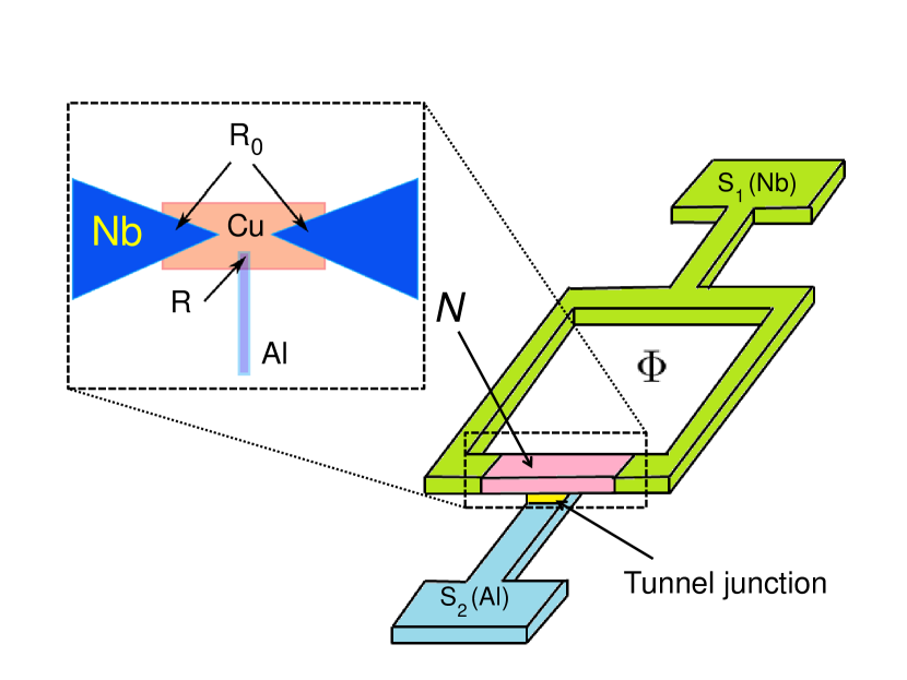
The operation of the device relies on the magnetic field modulation of the DoS Belzig1999 ; Belzig1996 ; Gueron1996 ; Sueur2008 in the proximized normal metal (N) Petrashov1994 ; Petrashov1995 ; Belzig2002 embedded between superconducting electrodes (), resulting in the opening of a minigap Belzig1999 ; Belzig1996 ; Zhou1998 in the N part. As shown in Fig. 1, the superconducting loop and probe are Nb and Al, respectively. A large number of applications has been proposed for SQUIPTs, similar to SQUIDs Clarke2004 ; Tinkham1996 ; Likharev1986 , including measurement of magnetic flux induced by atomic spins, single-photon detection and nanoelectronical measurements Foley2009 ; Hao2005 ; Hao2007 . The SQUIPT represents a sensitive interferometer with reduced power dissipation and potentially low flux noise in contrast to conventional SQUIDs Giazotto2010 ; Giazotto2011 . So far, a number of SQUIPT devices with an aluminum tunnel probe (S-SQUIPT) Giazotto2010 ; Meschke2011 ; Najafi2014 ; Ronzani2014 ; Najafi2016 ; Najafi2017 ; Ligato2017 ; Ronzani2017 ; Ambrosio2015 have been reported due to the high quality native oxide of Al, yielding excellent tunnel barriers Ligato2017 .
The flux sensitivity of a SQUIPT device can be improved by maximizing the proximity effect in the normal metal N, hence increasing the responsivity of the device to a change in magnetic field. In this respect, replacing the superconducting loop with a larger-gap superconductor such as vanadium Ligato2017 or niobium Najafi2016 is an evident direction to look for sensitive SQUIPTs. Recently, a device with normal-conducting probe (N-SQUIPT) has been shown to be a promising candidate for the implementation of SQUIPTs with very low dissipated power Ambrosio2015 . However, implementing low dissipation S-SQUIPTs has not been explored in detail up to now. Operating the S-SQUIPT at sub-gap bias voltages on the supercurrent branch allows to obtain extra-low power dissipation, reduced by up to two orders of magnitude compared to earlier devices Giazotto2010 ; Najafi2014 . In this article, we present a detailed experimental demonstration of Nb-Cu-Nb weak links and a SQUIPT based on a Nb superconducting loop (Nb-SQUIPT), first considered in Ref. 25. The devices are realized using an etching-based two-step fabrication process. We first characterize Nb-Cu-Nb junctions through low temperature switching current measurement and then investigate a Nb-SQUIPT, obtained by attaching an Al tunnel probe to the SNS weak link. In this prototype magnetometer, we observe the maximum flux-to-current transfer function value of about at , which has been measured close to zero bias voltage. Here, is the superconducting flux quantum.
2 Experimental methods and fabrication
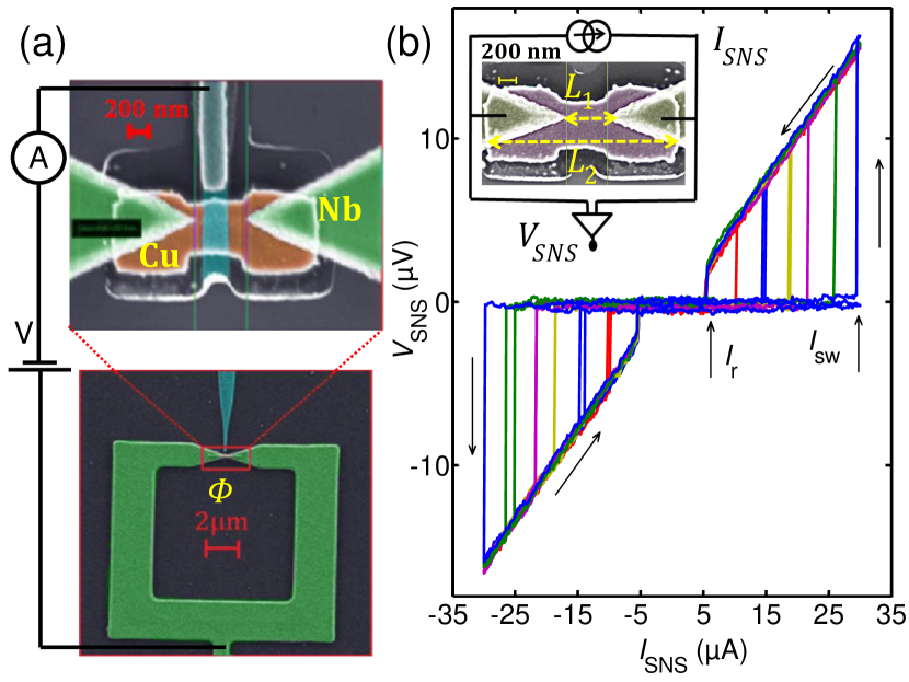
Both Nb-SQUIPT devices and Nb-Cu-Nb junctions on the same chip are fabricated using a process with two separate electron beam lithography (EBL) steps as discussed in detail in Ref. 25. The first step accomplishes patterning of the Nb structures. We start with an oxidized 4 inch Si wafer with 200 nm sputter-deposited Nb. In the first lithography step, we write into a layer of spin-coated positive tone AR-P 6200.13 resist. The lithography is followed by wet development and 5 min reflow baking at . In order to transfer the exposed pattern into the Nb film, reactive ion etching (RIE) is used with a mixture of and Ar. Nb etching is followed by the second EBL step using a conventional bilayer resist Dolan1977 , consisting of a 200 nm thick polymethyl methacrylate (PMMA) layer on top of a 900 nm layer of copolymer. This step provides the NIS tunnel junction and the Cu wire, and importantly, the clean electrical contacts between Nb and Cu in the Nb-Cu-Nb weak link.
The creation of a transparent contact between Nb and Cu is achieved by exposing the chip to Ar ion etching, prior to the Cu deposition in the same vacuum cycle. The Nb-Cu-Nb weak link and Nb-SQUIPT devices with an Al-AlOx-Cu Normal metalInsulatorSuperconductor (NIS) tunnel junction are simultaneously fabricated: After Ar etching, 25 nm of Al at an angle is deposited and oxidized for min at a pressure of mbar to form the tunnel barrier of the NIS probe. Next, approximately 25 nm Cu at is evaporated to complete the NIS junction and to form the normal metal wire. Figure 2shows a scanning electron microscope (SEM) image of a typical Nb-SQUIPT device with an enlarged view of the zone around the weak link. The measurements of the samples have been performed in a 3He/4He dilution refrigerator Pekola1994 down to the base temperature of about 80 mK.
3 Results and discussion
The relevant dimensions of a typical measured SNS structure [see inset of Fig. 2] are the minimum Nb electrode separation , the full length and minimum width of the Cu wire. We measure typical low temperature resistance value of the Cu strip to be about . In the diffusive SNS junction, the Thouless energy determines the energy scale for the proximity effect. Here and are the diffusion constant and the effective length of the Cu wire, respectively Giazotto2008 ; Blum2004 ; Dubos2008 . The effective length of the normal metal is derived from the estimated values of and the measured Cu diffusion constant Najafi2016 . The Nb-Cu-Nb sample considered here is in the long junction limit , where is the coherence length and the superconducting energy gap of Nb.
The current-voltage characteristic of the Nb-Cu-Nb structure is shown in the main panel of Fig. 2at different values of bath temperatures. The dc voltage is measured across the structure biased by a current in a four probe configuration as indicated in the inset of Fig. 2. As shown by the IV curves, the hysteretic behavior from self-heating in the finite-voltage state is observable at and hence the magnitudes of switching and retrapping current differ from each other. At the base temperature, we find them to be about and , respectively.
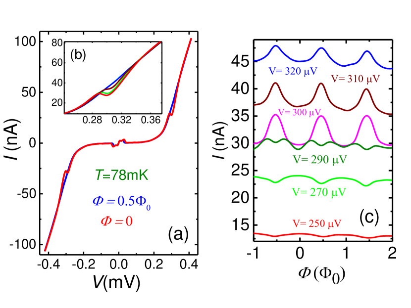
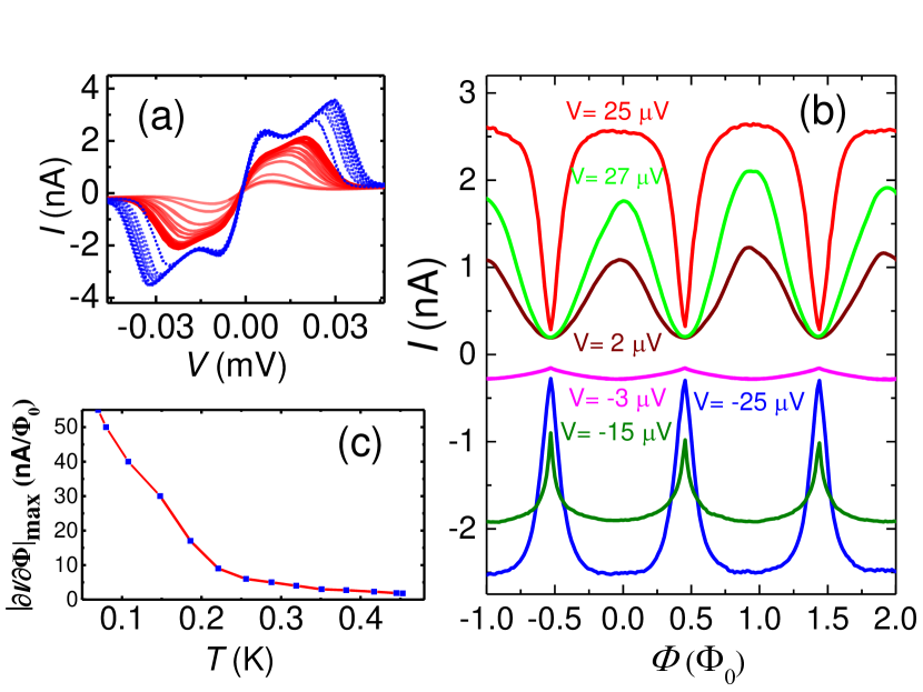
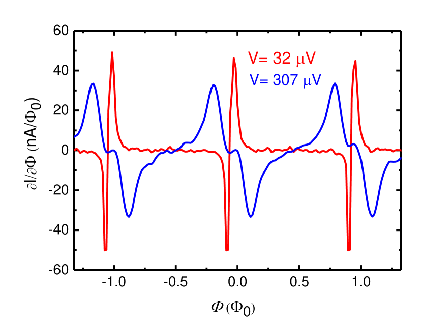
An IV characteristic of the Nb-SQUIPT is illustrated in Fig. 3, measured at two different magnetic fields, (red) and (blue), corresponding to maximum and minimum minigap opened in the normal weak link Sueur2008 ; Zhou1998 . Furthermore, the flux-dependent onset of current on the quasiparticle branch is shown in the inset when exceeds the sum of the probe electrode gap and the minigap induced in the N part. In the diffusive regime of a metallic SNS junction, the minigap in the normal metal is of the order of the Thouless energy Pannetier2000 . Considering the bias voltage dependence of the differential conductance Meschke2011 ; Najafi2014 and subtracting the contribution of an effective series resistance k, arising from the two point measurement technique, the magnitudes of the superconducting probe electrode gap and minigap are and , respectively. As a consequence of the minigap variations, the current is periodic as a function of the flux through the loop. Typical current modulations are displayed in Fig. 3for some selected values of bias voltages in the quasiparticle branch from to . Figure 3indicates that the measured current modulation reaches a peak-to-peak amplitude as large as at the bias voltage . We now consider the flux modulation in the low bias regime. Figure 4 demonstrates the extent of the flux modulation of the IV curve in the sub-gap regime close to zero bias at two different temperatures, mK (blue) and mK (red). At mK, almost full magnetic flux modulation of the IV is visible due to increased SNS weak link inductance in comparison to the loop inductance Ronzani2014 . We can furthermore observe current peak at the bias voltage V with the maximum current nA. It is caused by multiple Andreev reflections, which are visible due to relatively low tunnel resistance of the probe junction, k. In this sub-gap regime, the current modulation as a function of magnetic flux is shown in Fig. 4at few selected values of applied bias voltage. At , we find the maximum peak-to-peak amplitude as large as , corresponding to the maximum sensitivity . The effect of temperature on the flux-to-current transfer function is displayed in Fig. 4, showing the temperature dependence of the maximum sensitivity in the low bias regime. It decreases monotonously with increasing . For comparison, the transfer functions close to the optimum bias values in the supercurrent and quasiparticle regions are plotted in Fig. 5.
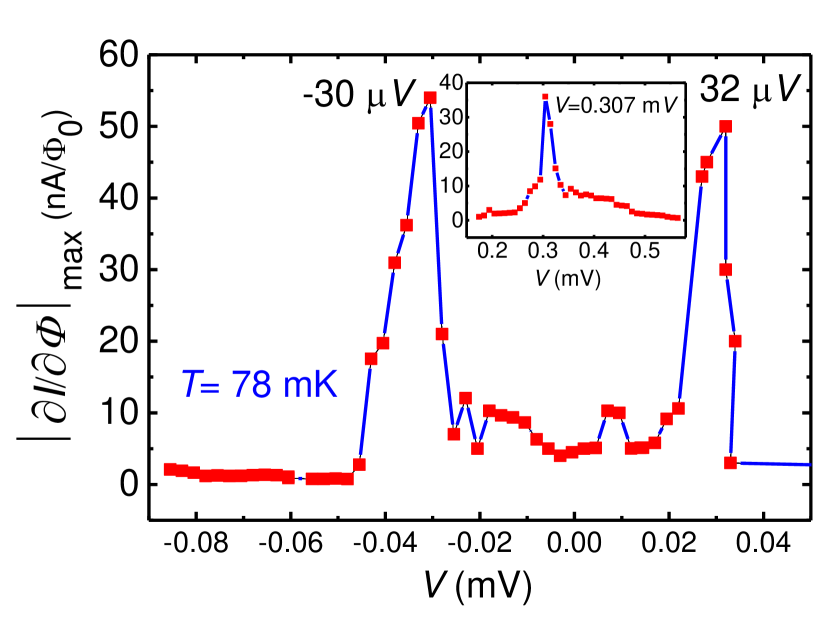
We now discuss the bias voltage dependence of the maximum sensitivity at the base temperature . Figure 6 indicates that the maximum current responsivity is obtained at , corresponding to . At this working point, the typical output current level is implying an average total power dissipation for the Nb-SQUIPT to be below . The value can be further reduced by simply increasing the resistance of the probing junction. This power is two orders of magnitude smaller than in our previous device with an Al superconducting probe Najafi2014 . The sub-gap operation of a SQUIPT is thus a possible choice for applications where very low dissipation is required.
Let us now briefly discuss the mechanism behind the SQUIPT response to the magnetic field at low bias. Considering first an ideal case, we assume that the response comes from the Josepshson current of the probe junction, which is modulated by the field together with the minigap in the copper island. The expected value of the critical current may be estimated by means of the Ambegaokar-Baratoff formula AB for an asymmetric junction with the gaps of the leads and . With the junction resistance k we find a maximum critical current nA.
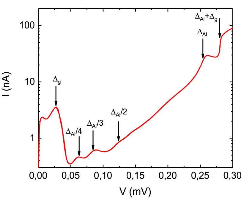
Assuming now that the minigap is modulated as , we can estimate the maximum responsivity of the device as nA/, which is about 10 times higher than in the experiment. Unfortunately, in our sample we observe only a very small critical current nA, which, on top of that, is not modulated by flux, and this simple mechanism is not working. However, our analysis shows that improving the quality of the probe junction may potentially increase the sensitivity of the SQUIPT. We believe that the observed low-bias current modulation in our device comes from multiple Andreev reflections (MAR). The tunnel barrier of the probe junction is rather transparent (overlap size , characteristic resistance ) and MAR signatures are clearly visible in the I-V curve plotted in Fig. 7. The observed pattern agrees well with the one expected for a junction between two different superconductors with the gaps and Cuevas . Namely, we find current peaks at , , a current jump at , and a series of less visible features at voltages , etc. In terms of responsivity at low bias, the MAR peak centered around V is important. The position of this peak follows the magnetic field dependent minigap , which results in the modulation of the current at fixed voltage shown in Fig. 4(b). The peak is smeared by increasing temperature and eventually vanishes at mK, see Fig. 4(c).
4 Summary
To summarize, we have investigated Nb-Cu-Nb weak links and, consequently, a Nb-SQUIPT at low bias voltages of the tunnel probe. The structures are based on a fabrication process with two independent lithography and deposition steps, relying on Ar ion cleaning of the Nb contact surfaces. The typical power dissipation in the fW range gives the opportunity of using the Nb-SQUIPT as a low dissipation magnetometer and, furthermore, in other detector applications such as ultrasensitive bolometers and calorimeters.
Acknowledgments
The work has been supported by the Academy of Finland (project numbers 284594 and 275167). We acknowledge Micronova Nanofabrication Centre of OtaNano research infrastructure for providing the processing facilities, and for the sputtered Nb films.
References
- (1) F. Giazotto, J. T. Peltonen, M. Meschke, and J. P. Pekola, Nat. Phys. 6, 254 (2010).
- (2) P. G. de Gennes, Rev. Mod. Phys. 36, 225 (1964).
- (3) P. G. de Gennes, Superconductivity of metals and alloys (W. A. Benjamin, 1966).
- (4) W. Belzig, F. K. Wilhelm, C. Bruder, G. Schön, and A. D. Zaikin, Superlatt. Microstruct. 25, 1251 (1999).
- (5) C. J. Lambert and R. Raimondi, J. Phy. Cond. Matt. 10, 901 (1998).
- (6) B. Pannetier and H. Courtois, J. Low Temp. Phys. 118, 599 (2000).
- (7) A. I. Buzdin, Rev. Mod. Phys. 77, 935 (2005).
- (8) W. Belzig, C. Bruder, and G. Schön, Phys. Rev. B 54, 9443 (1996).
- (9) S. Gueron, H. Pothier, Norman O. Birge, D. Esteve, and M. H. Devoret., Phys. Rev. Lett. 77, 3025 (1996).
- (10) H. le Sueur, P. Joyez, H. Pothier, C. Urbina, and D. Esteve, Phys. Rev. Lett. 100, 197002 (2008).
- (11) V. T. Petrashov, V. N. Antonov, P. Delsing, and T. Claeson, JETP Lett. 60, 606 (1994).
- (12) V. T. Petrashov, V. N. Antonov, P. Delsing, and T. Claeson, Phys. Rev. Lett. 74, 5268 (1995).
- (13) W. Belzig, R. Shaikhaidarov, V. V. Petrashov, and Yu. V. Nazarov, Phys. Rev. B. 66, 220505 (2002).
- (14) F. Zhou, P. Charlat, B. Spivak, and B. Pannetier, J. Low Temp. Phys. 110, 841 (1998).
- (15) J. Clarke, and A. I. Braginski, eds., The SQUID handbook: Applications of SQUIDs and SQUID systems, Volume I (Wiley-VCH, Wienheim, 2004).
- (16) M. Tinkham, , 2nd Ed. (McGraw-Hill, New York, 1996).
- (17) K. K. Likharev, Dynamics of Josephson Junctions and Circuits, 1st ed. (Gordon and Breach, 1986).
- (18) C. P. Foley and H. Hilgenkamp, Supercond. Sci. Technol. 22, 1 (2009).
- (19) L. Hao, J. C. Macfarlane, S. K. H. Lam, C. P. Foley, P. Josephs-Franks, and J. C. Gallop, IEEE Trans. Appl. Supercond. 15, 514 (2005).
- (20) L. Hao, J. C. Macfarlane, J. C. Gallop, D. Cox, P. Joseph-Franks, D. Hutson, and J. Chen, IEEE Trans. Instrum. Meas. 56, 392-395 (2007).
- (21) F. Giazotto, and F. Taddei, Phys. Rev. B 84, 214502 (2011).
- (22) M. Meschke, J. T. Peltonen, J. P. Pekola, and F. Giazotto, Phys. Rev. B 84, 214514 (2011).
- (23) R. N. Jabdaraghi, M. Meschke, and J. P. Pekola, Appl. Phys. Lett. 104, 082601 (2014).
- (24) A. Ronzani, C. Altimiras, and F. Giazotto, Phys. Rev. Appl. 2, 024005 (2014).
- (25) R. N. Jabdaraghi, J. T. Peltonen, O-P. Saira, and J. P. Pekola, Appl. Phys. Lett. 108, 042604 (2016).
- (26) R. N. Jabdaraghi, D. S. Golubev, J. P. Pekola, and J. T. Peltonen, Sci. Rep. 7, 8011 (2017).
- (27) N. Ligato, G. Marchegiani, P. Virtanen, E. Strambini, and F. Giazotto.
- (28) A. Ronzani, S. D’Ambrosio, R. Virtanen, F. Giazotto, and C. Altimiras, arxiv:1611.06263 (2016).
- (29) S. D’Ambrosio, M. Meissner, C. Blanc, A. Ronzani, and F. Giazotto, Appl. Phys. Lett. 107, 113110 (2015).
- (30) G. J. Dolan, Appl. Phys. Lett. 31, 337 (1977).
- (31) J. P. Pekola and J. P. Kauppinen, Cryogenics 34, 843 (1994).
- (32) F. Giazotto, T. T. Heikkilä, G. Pepe, P. Helistö, A. Luukanen, and J. P. Pekola, Appl. Phys. Lett. 92, 162507 (2008).
- (33) Y. Blum, A. Tsukernik, M. Karpovski, and A. Palevski, Phys. Rev. B 70, 214501 (2004).
- (34) P. Dubos, H. Courtois, B. Pannetier, F. K. Wilhelm, A. D. Zaikin, and G. Schön, Phys. Rev. B 63, 064502 (2001).
- (35) V. Ambegaokar and A. Baratoff, Phys. Rev. Lett. 10, 486 (1963).
- (36) M. Ternes, W.D. Schneider, J.C. Cuevas, C.P. Lutz, C.F. Hirjibehedin, and A.J. Heinrich, Phys. Rev. B 74, 132501 (2006).