ZnO Defect Modulation for Efficient Photocatalysis
Abstract
We have investigated the combined effect of low-energy self-implantation and thermal annealing on the near-surface defect concentration of ZnO single-crystals. Using ionoluminescence (IL), we demonstrate that a combination of low-energy low-fluence Zn and O ion implantation followed by annealing in Ar increases the near-surface point defect concentration in ZnO by two orders of magnitude. Point defects are known to increase the surface reactivity of ZnO, thereby improving the efficiency of ZnO photocatalytic processes such as bilirubin degredation. We hereby provide recommendations on how to improve the efficiency of ZnO-related photocatalytic processes.
keywords:
Ion implantation, Point defects, Ionoluminescence, ZnO , Annealing , CatalysisPACS:
78.60.Hk , 61.72.uj , 61.72.-y , 71.55.Gs , 82.65.+r1 Introduction
Toxic wastes substances, ranging from industrial effluents to metabolic bi-products, are matters of serious health and environmental concern. Photocatalysis is currently an important eco-friendly and cost effective method for such waste treatment.
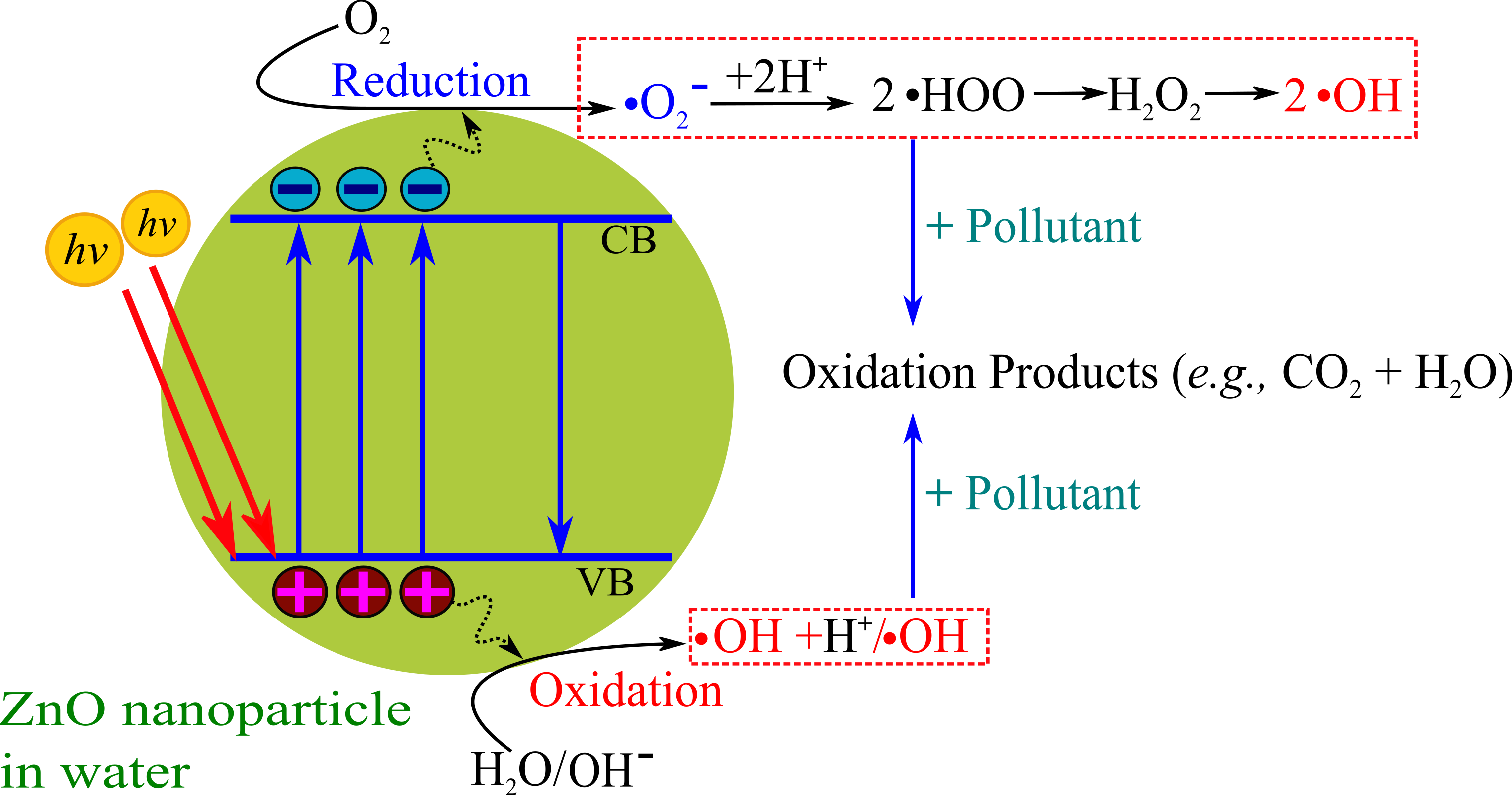
In an ideal photocatalytic process, organic pollutants are mineralized into \ceCO2, \ceH2O and mineral acids in the presence of a photocatalyst, typically a metallic oxide semiconductor, and an oxidizing species such as air. When semiconductors are exposed to light in solution, electrons-hole (e-h) pairs are generated. These e-h pairs aid the splitting of water into the hydroxyl (\ce⋅OH) and superoxide (\ce⋅O2-) radicals. \ce⋅OH is an extremely strong non-selective oxidant which leads to partial or complete mineralization of most organic pollutants. A typical photocatalytic process is illustrated in Fig. 1.
Commonly used metal oxide semiconductors for photocatalysis are titanium dioxide (\ceTiO2), ZnO, tungsten oxide (\ceWO3), strungtium titanate (\ceSrTiO3) and hematite (-\ceFe2O3). Of these, ZnO is particularly attractive for photocatalysis due to a number of reasons. Firstly, ZnO is biocompartible, biodegradable and non-toxic [1]. Secondly, it has a high surface reactivity induced by native point defects [2]. Thirdly, the ability to tune ZnO band gap through doping [3] gives it a higher photoefficiency in direct sunlight whose UV composition on Earth is significanlty low (4-7 %). Lastly, ZnO is inexpensive and its nanostructures can be easily synthesized using a variety of methods.
Recently, Bora et al. [4] investigated bilirubin (BR) degradation in the presence of ZnO nanoparticles and UV light. They directly showed that ZnO nano-structures with a higher near-surface defect (particularly oxygen vacancy) concentration greatly accelerated bilirubin degredation in the presence of UV light, Fig. 2. Paradoxically, the primary method for oxygen vacancy () generation in ZnO for Bora and co-workers was by thermal annealing of ZnO in air (\ceO2). But, first-principle calculations show that the formation energy E\tsf of VO in excess O is relatively high compared to that of VO in excess Zn [5]. Therefore, thermal annealing of ZnO in \ceO2 is not the best approach for enhancing the near-surface concentration in ZnO for photocatalytic purposes.
In a recent study [6], we demonstrated that a judicious combination of ion implantation and thermal annealing can better enhance the near surface defect concentration of ZnO.
We hereby investigate the combined effect of low-energy ion implantation and thermal annealing on the near-surface defect concentration of ZnO single-crystals. Our results show that the near-surface defect concentration in ZnO can be significantly enhanced through a careful combination of self-implantation and thermal annealing in Ar. Particularly, we show that by simply annealing pristine ZnO in \ceAr at 1000 °C for 1 hour, the near surface defect concentration increases by a factor of 30. Annealing ZnO in \ceO2 under similar conditions show a defect enhancement factor of only 7. These findings provide new perspectives on the efficiency enhancement of photocatalytic processes.

2 Experiment
Double-face EPI-polished mm wafers of hydrothermally grown (MTI Corporation, Richmond, CA) c-plane ZnO single-crystals were used in this experiment. Sample purity was greater than with minute traces of Mg , Al , Si , Ti , Cu , Fe , Ca , and Ag , according to the supplier. The Zn face of eight samples was modified by 60 keV self-implantation and thermal annealing as described on Table 1.
| Sample name | 60 keV Implantation | Annealing in 1 atm |
|---|---|---|
| ZnO | none (virgin) | none |
| ZnOO2 | none (virgin) | 1000 °C in O2, 1 hr |
| ZnOAr | none (virgin) | 1000 °C in Ar, 1 hr |
| ZnO:8O | O\ts-/ | none |
| ZnO:8Zn | Zn\ts-/ | none |
| ZnO:8OAr | O\ts-/ | 1000 °C in Ar, 1 hr |
| ZnO:8ZnAr | Zn\ts-/ | 1000 °C in Ar, 1 hr |
| ZnO:16OAr | O\ts-/ | 1000 °C in Ar, 1 hr |
| ZnO:16ZnAr | Zn\ts-/ | 1000 °C in Ar, 1 hr |
Implantations were carried out in a vacuum chamber with pressure Torr. The O\ts- and Zn\ts- beam current densities were 6 A cm\ts-2 and 0.24 A cm\ts-2, respectively. Ion beams were generated by a source for negative ions by cesium sputtering (SNICS) [7]. For all practical purposes, it does not matter whether implantation is made with positive or negative ions. To restore bulk crystallinity while simultaneously increasing the near-surface point defect concentration, samples were annealed under Ar and \ceO2 at 1000 °C. All samples were then irradiated by 2 MeV He\ts+ ions and the resultant ionoluminescent (IL) spectra obtained. Details of the IL process are described in Ref. [6]. IL spectra for all samples were then analysed.
The relative near-surface defect concentration for each sample was monitored using an enhancement parameter defined by
| (1) |
where and are the green-yellow and UV luminescent band intensities, respectively. The smaller this ratio is, the better the crystalline quality [8].
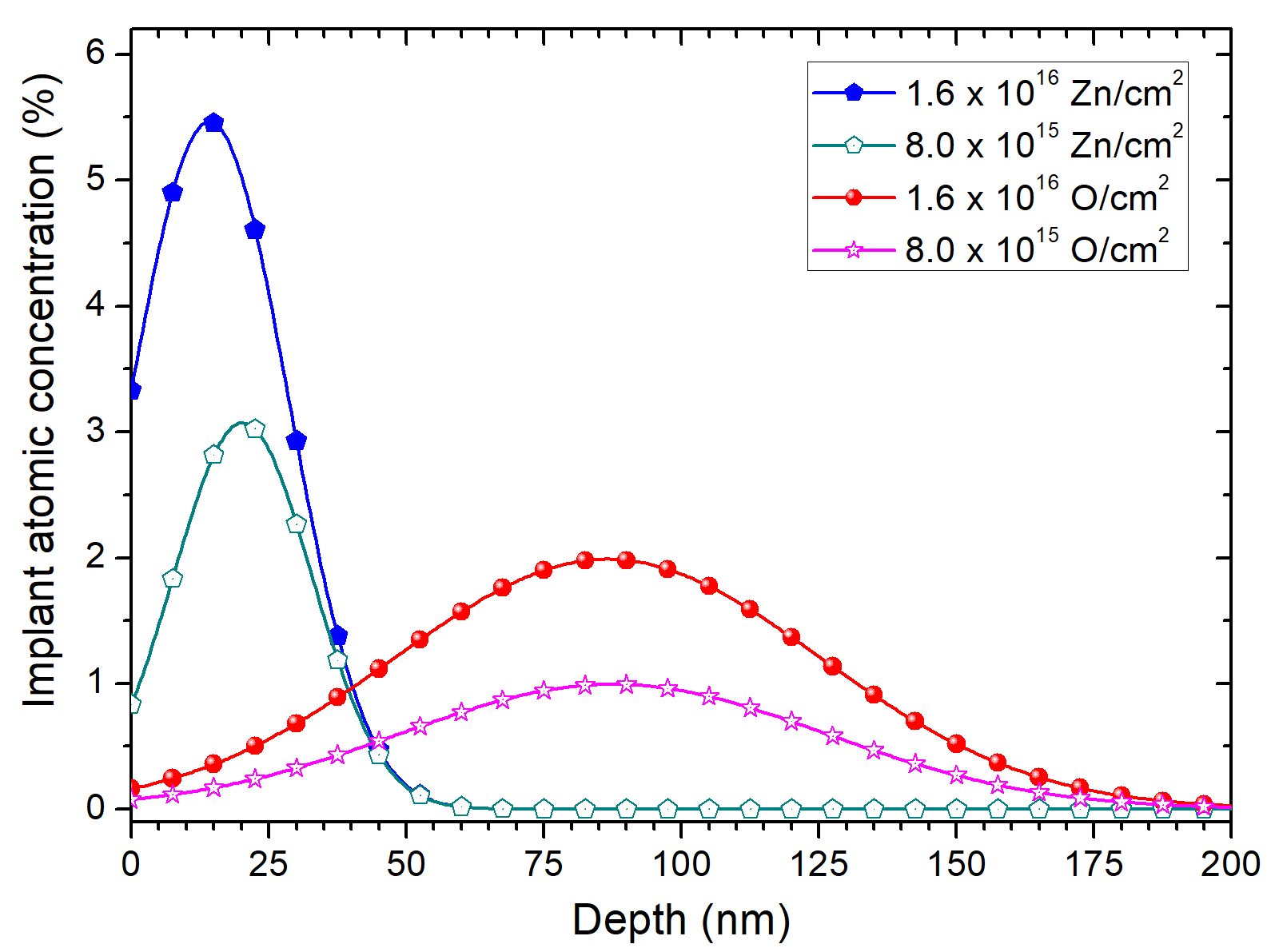
At high fluences ( \cecm^-2), sputtering, and ion-beam induced migration of atoms can significantly reduce the projected range and ion concentration. Thus, fluence-dependent depth distribution for implant species was estimated using the equation, [9, 10]:
| (2) |
where is the depth coordinate with respect to the instantaneous target (or substrate) surface, is the atomic density of the substrate, is the sputtering yield, is the range straggling related to and “” is the error function. All fitting parameters to Eq. 2 were obtained from computer simulations with the SRIM2008 [11] code.
3 Results and Analysis
3.1 SRIM Analysis
Fig. 3 shows the fluence-dependent implant distribution based on Eq. 2. While the projected range for O implants remain constantly at 87 nm, that for Zn implant shifts towards the surface from 20 nm to 15 nm as fluence doubles from . This is due to the relatively high sputtering rate of ZnO induced by Zn ions. In fact, under our experimental conditions, the estimated sputtering yields due to Zn\ts- and O\ts- ions are 13 atoms/ion and 2 atoms/ion, respectively. Although Zn and O implant concentrations roughly double as corresponding fluences double, Zn implants at high fluence are likely to reach the ZnO target surface earlier and anneal out faster than those at low fluence upon heat treatement. This is due to smaller instantaneous Rp, narrower distribution profile and higher mobility of compared to low fluence Zn and O implants.
3.2 IL Analysis
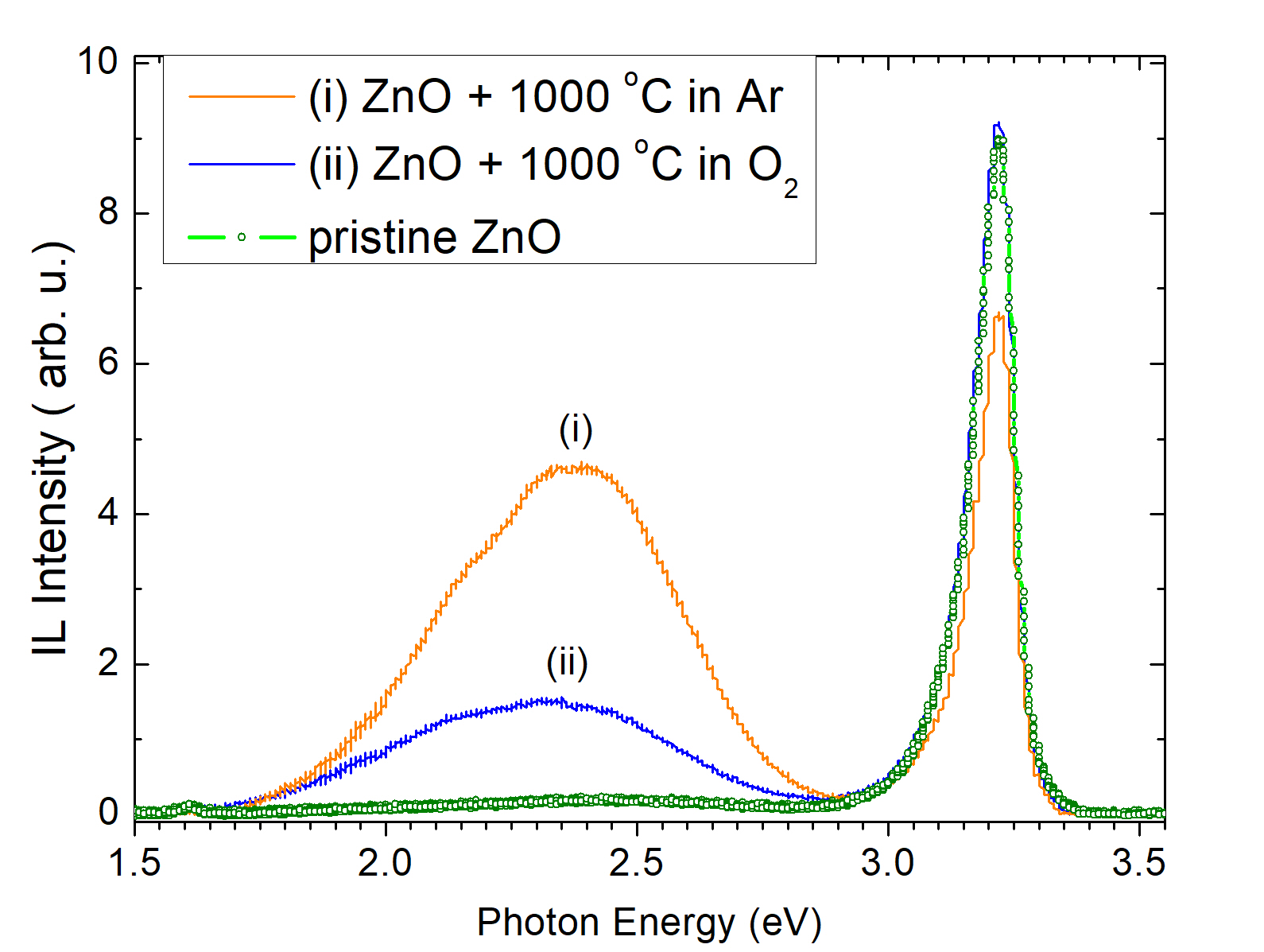
Fig. 4 compares the IL spectrum of pristine ZnO with those of ZnO annealed under ambient Ar and O2 at 1000 °C for 1 hr. All samples display three peaks, characteristic of ZnO: a sharp UV emission peak centered around 3.2 eV, a broad green-yellow emission peak centered around 2.4 eV, and a small red emission peak centered around 1.6 eV. We observe significant enhancement of Ig-y for the annealed samples compared to pristine ZnO. A low Ig-y and correspondingly high Iuv in the pristine sample signifies very small near-surface defect concentration in agreement with the high crystalline quality of this pristine sample. On the other hand, the high Ig-y for annealed ZnO samples indicate an increase in their near-surface defect concentration. Particularly, Ig-y(ZnOAr) = 3 Ig-y(ZnOO2) suggesting that the near surface defect concentration in ZnOAr is at least 3 times that in ZnOO2 (i.e., ).
Previously we demonstrated that the 2.4 eV peak is mostly related to near surface VO and presumably concentrations [6]. Although both defects have almost the same defect-formation energy E\tsf, according to first principle calculations [5], the defect-migration-barrier potential for Zni is lower than that for VO. Thus, Zni are more mobile than VO. This implies that both defects are created with equal ease but Zni are likely to anneal faster. Therefore, we deduce that the the luminescent effect of Zni on the 2.4 eV peak is minimal.
During ZnO annealing under ambient \ceO2, the rate of near-surface VO annihilation is enhanced. This is because ambient \ceO2 diffuses into the ZnO bulk recombining with some VO. This explains why Ig-y(ZnOAr) = 3 Ig-y(ZnOO2).

Ion implantation is another effective method of introducing point defects in ZnO. Fig. 5 compares the IL spectra of \ceZn^- and \ceO^- implanted ZnO with that of pristine ZnO single-crystal. A drop in Iuv for as-implanted samples clearly indicates the presence of point defects resulting from radiation damage. Paradoxically, there is no corresponding enhancement of Ig-y. This is due to the intensification of competitive non-radiation pathways induced by stress fields generated in the implantation layer. Thermal annealing is an effective way to relax bonds thereby suppressing these non-radiation pathways.

Fig. 6 shows the effect of thermal annealing on the IL spectra of self-implanted ZnO single-crystals. We observe significant equal enhancement of Ig-y for both the ZnO:8OAr and ZnO:8ZnAr samples. In fact, Ig-y for both samples is more than 3 times that for the ZnOAr sample and more than 9 times that for the \ceO2 annealed ZnO shown in Fig. 4. On the other hand, Iuv for both ZnO:8OAr and ZnO:8ZnAr samples is slightly less than that for pristine ZnO. Using Eq. 1, we estimate the relative defect concentration ratios for ZnO:8OAr and ZnO:8ZnAr samples at 56 and 72 respectively; being the near-surface defect parameter for pristine ZnO.

Fig. 7 shows the effect of doubling Zn and O implant fluence followed by thermal annealing. We observe that by doubling the implantation fluence to , Ig-y(ZnO:16OAr) remains high while Ig-y(ZnO:16ZnAr) drops relative to ZnO:8ZnAr. However, these changes are accompanied by corresponding decrease in both Iuv. Using Eq. 1, the relative defect concentrations for ZnO:16OAr and ZnO:16ZnAr are respectively 125 and 104. These values are almost double those obtained for samples ZnO:8OAr and ZnO:8ZnAr.
4 Summary and Conclusions
We have used a combination of thermal annealing, and low-energy self-implantation to modulate the near-surface native-point-defect concentration of ZnO single-crystals. Using ion beam induced luminescence, we have estimated the near-surface defect enhancement factor of our modified samples. Our results are summarised in Table 2. We observe that by simply annealing pristine ZnO single-crystals in \ceO2 and Ar, their near surface defect concentration, relative to pristine ZnO, increase by factors of 7 and 30, respectively. Low-energy self-implantation followed by thermal annealing further increases the samples’ near-surface defect concentration upto 125 times that of pristine ZnO.
| Sample name | Ig-y | Iuv | ||
|---|---|---|---|---|
| ZnO | 0.216 | 9.011 | 0.024 | 1 |
| ZnOO2 | 1.529 | 9.203 | 0.166 | 7 |
| ZnOAr | 4.674 | 6.672 | 0.701 | 30 |
| ZnO:8O | 0.261 | 2.362 | 0.110 | / |
| ZnO:8Zn | 0.060 | 5.814 | 0.010 | / |
| ZnO:8OAr | 15.288 | 11.408 | 1.340 | 56 |
| ZnO:8ZnAr | 15.612 | 9.014 | 1.732 | 72 |
| ZnO:16OAr | 16.373 | 5.444 | 3.008 | 125 |
| ZnO:16ZnAr | 8.297 | 3.22 | 2.498 | 104 |
Thus, we an effective practical method for enhancing the photocatalytic activity of ZnO nano-structures in large scale applications is to anneal them under ambient Ar rather than \ceO2. Furthermore, irradiating ZnO nano-structures with low-energy low-fluence \ceO^- or \ceZn^- ions followed by thermal annealing in Ar will greatly enhance their photocatalytic efficiency by even higher others of magnitude.
5 Acknowledgments
This work was funded by the state of Texas through the Texas Center for Superconductivity at the University of Houston.
References
References
- Zhou et al. [2006] J. Zhou, N. Xu, Z. L. Wang, Adv. Mater. 18 (2006) 2432.
- Ali et al. [2010] A. M. Ali, E. A. C. Emmanuelsson, D. A. Patterson, Appl. Catal., B 97 (2010) 2010.
- Abdollahi et al. [2011] Y. Abdollahi, A. H. Abdullah, Z. Zainal, N. A. Yusof, Int. J. Basic Appl. Sci 11 (2011) 44.
- Bora et al. [2013] T. Bora, K. K. Lakshman, S. Sarkar, A. Makhal, S. Sardar, S. K. Pal, J. Dutta, Beilstein J. Nanotechnol. 4 (2013) 714.
- Janotti and Van de Walle [2007] A. Janotti, C. G. Van de Walle, Phys. Rev. B 76 (2007) 165202.
- Epie and Chu [2016] E. N. Epie, W. K. Chu, Appl. Surf. Sci. 371 (2016) 28.
- Middleton [1983] R. Middleton, Nucl. Instrum. Methods B 214 (1983) 139.
- Willander et al. [2010] M. Willander, O. Nur, J. R. Sadaf, M. I. Qadir, S. Zaman, A. Zainelabdin, N. Bano, I. Hussain, Materials 3 (2010) 2643.
- Wang et al. [2013] J. Wang, G. Jia, B. Zhang, H. Liu, C. Liu, J. Appl. Phys. 113 (2013) 034304.
- Gnaser et al. [2008] H. Gnaser, A. Brodyansky, B. Reuscher, Surf. Interface Anal. 40 (2008) 1415.
- Ziegler et al. [2008] J. F. Ziegler, J. P. Biersack, M. D. Ziegler, SRIM - The Stopping and Range of Ions in Matter, Ion Implantation Press, http://www.lulu.com/content/1524197, 2008.