Kapitza thermal resistance across individual grain boundaries in graphene
Abstract
We study heat transport across individual grain boundaries in suspended monolayer graphene using extensive classical molecular dynamics (MD) simulations. We construct bicrystalline graphene samples containing grain boundaries with symmetric tilt angles using the two-dimensional phase field crystal method and then relax the samples with MD. The corresponding Kapitza resistances are then computed using nonequilibrium MD simulations. We find that the Kapitza resistance depends strongly on the tilt angle and shows a clear correlation with the average density of defects in a given grain boundary, but is not strongly correlated with the grain boundary line tension. We also show that quantum effects are significant in quantitative determination of the Kapitza resistance by applying the mode-by-mode quantum correction to the classical MD data. The corrected data are in good agreement with quantum mechanical Landauer-Bütticker calculations.
keywords:
Grain boundary , Kapitza resistance , Graphene , Molecular dynamics , Phase field crystal1 Introduction
Graphene [1], the famous two-dimensional allotrope of carbon, has been demonstrated to have extraordinary electronic [2], mechanical [3], and thermal [4] properties in its pristine form. However, large-scale graphene films, which are needed for industrial applications are typically grown by chemical vapor deposition [5] and are polycrystalline in nature [6], consisting of domains of pristine graphene with varying orientations separated by grain boundaries (GB) [7, 8, 9]. They play a significant or even dominant role in influencing many properties of graphene [10, 11].
One of the most striking properties of pristine graphene is its extremely high heat conductivity, which has been shown to be in excess of W/mK [4, 12]. Grain boundaries in graphene act as line defects or one-dimensional interfaces which leads to a strong reduction of the heat conductivity in multigrain samples [13, 14]. The influence of GBs can be quantified by the Kapitza or thermal boundary resistance . The Kapitza resistance of graphene grain boundaries has been previously computed using molecular dynamics (MD) [15, 16] and Landauer-Bütticker [17, 18] methods, and has also been measured experimentally [19]. However, these works have only considered a few separate tilt angles, and a systematic investigation on the dependence of the Kapitza resistance on the tilt angle between any two pristine grains is still lacking. The relevant questions here concern both the magnitude for different tilt angles and possible correlations between the structure or line tension of the GBs and the corresponding value of .
Modelling realistic graphene GBs has remained a challenge due to the multiple length and time scales involved. Recently, an efficient multiscale approach [20] for modelling polycrystalline graphene samples was developed based on phase field crystal (PFC) models [21, 22]. The PFC models are a family of continuum methods for modelling the atomic level structure and energetics of crystals, and their evolution at diffusive time scales (as compared to vibrational time scales in MD). The PFC models retain full information about the atomic structure and elasticity of the solid [22]. It has been shown [20] that using the PFC approach in two-dimensional space one can obtain large, realistic and locally relaxed microstructures that can be mapped to atomic coordinates for further relaxation in three-dimensional space with the usual atomistic simulation methods.
In this work, we employ the multiscale PFC strategy of Ref. [20] to generate large samples of tilted, bicrystalline graphene with a well-defined GB between the two grains. These samples are then further relaxed with MD at K. A heat current is generated across the bicrystals using nonequilibrium MD (NEMD) simulations, and the Kapitza resistance is computed from the temperature drop across the GB. We map the values of for a range of different tilt angles and demonstrate how correlates with the structure of the GBs. Finally, we demonstrate that quantum corrections need to be included in to obtain quantitative agreement with experiments and lattice dynamical calculations.
2 Models and Methods
2.1 PFC models
PFC approaches typically employ a classical density field to describe the systems. The ground state of is governed by a free energy functional that is minimized either by a periodic or a constant , corresponding to crystalline and liquid states, respectively. We use the standard PFC model
| (1) |
where the model parameters and are phenomenological parameters related to temperature and average density, respectively. The component penalizes for deviations from the length scale set by the wave number , giving rise to a spatially oscillating and to elastic behaviour [21, 22]. The crystal structure in the ground state is dictated by the formulation of and the average density of , and for certain parameter values the ground state of displays a honeycomb lattice of density maxima as appropriate for graphene [20].
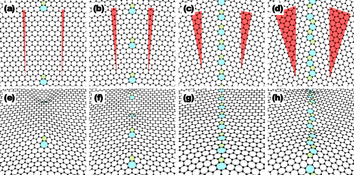
The PFC calculations are initialized with symmetrically tilted -crystals in a periodic, two-dimensional computational unit cell. The initial guess for the crystalline grains is obtained by using the one-mode approximation [22]
| (2) |
and by rotating alternatingly by . The tilt angle between two adjacent grains is , which ranges from to (see Fig. 1 for examples). We consider a subset of the tilt angles investigated in Ref. [20], with the exact values being listed in Table 1. The rotated grains and the unit cell size are matched together as follows: if just one of the rotated grains filled the whole unit cell, it would be perfectly continuous at the periodic edges. Along both interfaces, narrow strips a few atomic spacings wide are set to the average density – corresponding to a disordered state – to give the grain boundaries some additional freedom to find their lowest-energy configuration. We assume non-conserved dynamics to relax the systems in analogy to chemical vapour deposition [23] – the number of atoms in the monolayer can vary as if due to exchange with a vapor phase. In addition, the unit cell dimensions are allowed to vary to minimize strain. Further details of the PFC calculations can be found in Ref. [20]. The relaxed density field is mapped to a discrete set of atomic coordinates suited for the initialization of MD simulations [20].
2.2 NEMD simulations
We use the NEMD method as implemented in the GPUMD (graphics processing units molecular dynamics) code [24, 25, 26] to calculate the Kapitza resistance, using the Tersoff [27] potential with optimized parameters [28] for graphene. The initial structures obtained by the PFC method are rescaled by an appropriate factor to have zero in-plane stress at 300 K in the MD simulations with the optimized Tersoff potential [28].
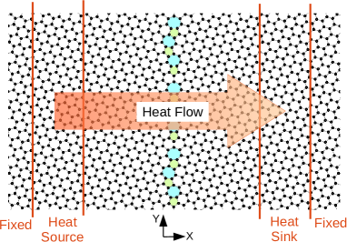
In the NEMD simulations, periodic boundary conditions are applied in the transverse direction, whereas fixed boundary conditions are applied in the transport direction. We first equilibrate the system at 1 K for 1 ns, then increase the temperature from 1 K to 300 K during 1 ns, and then equilibrate the system at 300 K for 1 ns. After these steps, we apply a Nosé-Hoover chain of thermostats [29, 30, 31] to the heat source and sink, choosing as two blocks of atoms around the two ends of the system, as schematically shown in Fig. 2. The temperatures of the heat source and sink are maintained at 310 K and 290 K, respectively. We have checked that steady state can be well established within 5 ns. In view of this, we calculate the temperature profile of the system and the energy exchange rate between the system and the thermostats using data sampled in another 5 ns. The velocity-Verlet integration scheme [32] with a time step of 1 fs is used for all the calculations. Three independent calculations are performed for each system and the error estimates reported in Table 1 correspond to the standard error of the independent results.
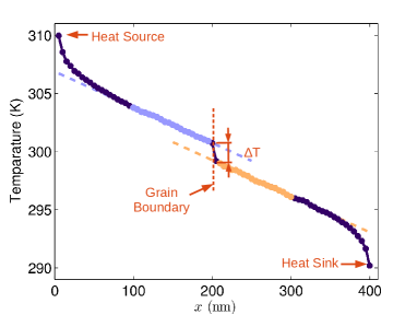
In steady state, apart from the nonlinear regions around the heat source and the sink intrinsic to the method, a linear temperature profile can be established on each side of the GB, but with an inherent discontinuity (temperature jump) at the GB. An example of this for the system with is shown in Fig. 3. The Kapitza resistance is defined as the ratio of the temperature jump and the heat flux across the grain boundary:
| (3) |
where can be calculated from the energy exchange rate (between the system and thermostat) and the cross-sectional area (graphene thickness is chosen as nm in our calculations), i.e. .
3 Results and Discussion
| () | (K) | (GW/m2) | (m2K/GW) | (nm) | (eV/nm) | (1/nm) |
|---|---|---|---|---|---|---|
| 1.10 | 0.55 | 0.08 | ||||
| 4.41 | 2.21 | 0.31 | ||||
| 9.43 | 3.84 | 0.67 | ||||
| 13.17 | 4.71 | 0.93 | ||||
| 18.73 | 5.02 | 1.32 | ||||
| 21.79 | 4.69 | 1.54 | ||||
| 27.80 | 4.71 | 1.95 | ||||
| 32.20 | 3.77 | 2.25 | ||||
| 36.52 | 4.93 | 1.91 | ||||
| 42.10 | 5.50 | 1.46 | ||||
| 46.83 | 5.16 | 1.06 | ||||
| 53.60 | 3.36 | 0.52 | ||||
| 59.04 | 0.61 | 0.08 |
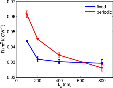
It is well known [33, 15, 16] that the calculated Kapitza resistance depends on the sample length in NEMD simulations. Figure 4 shows the calculated Kapitza resistance in the case as a function of the sample length . Using fixed boundary conditions as described above, saturates at around nm. On the other hand, using periodic boundaries as described in Ref. [15], converges more slowly. To this end, we have here used fixed boundary conditions and a sample length of nm for all the systems. The calculated temperature jump , heat flux , and Kapitza resistance in the 13 bicrystalline systems are listed in Table 1.
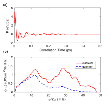
The Kapitza resistance calculated from the heat flux does not contain any information on the contributions from individual phonon modes. Methods of spectral decomposition of both the heat current (flux) [37, 38, 39, 40, 41, 42] and the temperature [43] within the NEMD framework have been developed recently. Here, we use the spectral decomposition formalism as described in Ref. [42] to calculate the spectral conductance of the system. In this method, one first calculates the following nonequilibrium heat current correlation function ( is the correlation time):
| (4) |
where and are respectively the potential energy and velocity of particle , ( is the position of particle ), and measures the heat current flowing form a block to an adjacent block arranged along the transport direction. Then, one performs a Fourier transform to get the spectral conductance:
| (5) |
The spectral conductance is normalized as
| (6) |
where is the total Kapitza conductance (also called thermal boundary conductance), which is the inverse of the Kapitza resistance .
Figure 5(a) shows the calculated correlation function , which resembles the velocity autocorrelation function whose Fourier transform is the phonon density of states [44]. Indeed, thermal conductance in the quasi-ballistic regime is intimately related to the phonon density of states. The corresponding spectral conductance is shown as the solid line in Fig. 5(b). The total thermal boundary conductance is GW/m2/K, corresponding to a Kapitza resistance of m2K/GW.
In view of the high Debye temperature (around K) for pristine graphene [45], we expect that it is necessary to correct the classical results to properly account for possible quantum effects. While using classical statistics can lead to [46] an underestimate of the scattering time for the low-frequency phonons as well as an overestimate of the heat capacity of the high-frequency phonons for thermal transport in the diffusive regime, only the second effect matters here in the quasi-ballistic regime. Therefore, one can correct the results by multiplying the classical spectral conductance by the ratio of the quantum heat capacity to the classical one: , where , with , , being the Planck constant, Boltzmann constant, and system temperature, respectively. This factor is unity in the low-frequency (high-temperature) limit and zero in the high-frequency (low-temperature) limit. Applying this mode-to-mode quantum correction to the classical spectral conductance gives the quantum spectral conductance represented by the dashed line in Fig. 5(b). The integral of the quantum corrected spectral conductance is reduced by a factor of about as compared to the classical one.
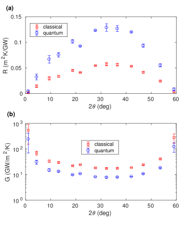
Figure 6(a) shows the calculated Kapitza resistances for all the systems as a function of the tilt angle, both before (red squares) and after (blue circles) applying the quantum correction. It clearly shows that the Kapitza resistance depends strongly on the tilt angle, varying by more than one order of magnitude. The Kapitza resistance increases monotonically from both sides to the middle angle of , except for one “anomalous” system with . This system has smaller than that with . One intuitive explanation is that this system is relatively flat compared to other systems, as can been seen from Figs. 1(e)-(h). Similar “anomalous” heat transport has been reported in Ref. [47] for the same grain boundary tilt angle.
The largest Kapitza resistances occurring around the intermediate angles, being about m2/K/GW after quantum corrections, are more than an order of magnitude smaller than those in grain boundaries in silicon nanowires [36]. A more reasonable comparison between different materials is in terms of the Kapitza length [48], defined as the system length of the corresponding pristine material at which the bulk thermal resistance due to phonon-phonon scattering equals the Kapitza resistance. Mathematically, we have
| (7) |
where is the thermal conductivity of the bulk material. We calculate by assuming a value of W/mK for pristine graphene according to the very recent experiments [12] and list the values in Table 1. The largest Kapitza lengths (corresponding to the largest Kapitza resistances) before quantum corrections are about 300 nm, which would be about 700 nm after quantum corrections. These values are actually larger than those for silicon nanowires. Therefore, the effect of grain boundaries on heat transport in graphene is not small even though the Kapitza resistances are relatively small.
To facilitate comparison with previous works, we also show the Kapitza conductances in Fig. 6(b). The Kapitza conductances in our systems range from about 17 GW/m2/K to more than 500 GW/m2/K before applying the quantum corrections. Bagri et al. [15] reported Kapitza conductance values (obtained by NEMD simulations with periodic boundary conditions in the transport direction) ranging from 15 GW/m2/K to 45 GW/m2/K. The lower limit of 15 GW/m2/K does not conflict with our data, as this value is reported in a system of a grain size of 25 nm, where the data cannot have converged yet. On the other hand, Cao and Qu (obtained by NEMD simulations with fixed boundary conditions in the transport direction) [16] reported saturated Kapitza conductance values in the range of GW/m2/K, which fall well within the values that we obtained. Last, we note that quantum mechanical Landauer-Bütticker calculations by Serov et al. [18] predicted the Kapitza conductance to be about 8 GW/m2/K for graphene grain boundaries comparable to those in our samples with intermediate tilt angles (). This is much smaller than the classical Kapitza conductances (about 20 GW/m2/K), but agree well with our quantum corrected values. This comparison justifies the mode-to-mode quantum correction we applied to the classical data and resolves the discrepancy between the results from classical NEMD simulations and quantum mechanical Landauer-Bütticker calculations.
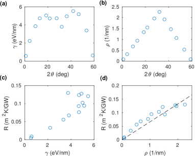
The last remaining issue concerns the possible correlation of the values of with the energetics and structure of the GBs. The grain boundary line tension and the defect density are closely related to the tilt angle. The line tension is defined as
| (8) |
in the thermodynamic limit, where is the formation energy for a GB of length . The defect density is defined as
| (9) |
where is the number of pentagon-heptagon pairs in the grain boundary. The calculated and values for all the tilt angles are listed in Table 1 and plotted in Figs. 7(a)-(b). In Figs. 7(c)-(d), we plot the Kapitza resistance against and , respectively. At small and large tilt angles, where the defect density is relatively small, there is a clear linear dependence of on both and . However, at intermediate tilt angles (), where the defect density is relatively large, the linear dependences become less clear, especially between and , which may indicate increased interactions between the defects. Overall, there is a stronger correlation between the Kapitza resistance and the defect density which is consistent with the idea of enhanced phonon scattering with increasing .
4 Summary and Conclusions
In summary, we have employed an efficient multiscale modeling strategy based on the PFC approach and atomistic MD simulations to systematically evaluate the Kapitza resistances in graphene grain boundaries for a wide range of tilt angles between adjacent grains. Strong correlations between the Kapitza resistance and the tilt angle, the grain boundary line tension, and the defect density are identified. Quantum effects, which have been ignored in previous studies, are found to be significant. By applying a mode-to-mode quantum correction method based on spectral decomposition, we have demonstrated that good agreement between the classical molecular dynamics data and the quantum mechanical Landauer-Bütticker method can be obtained.
We emphasize that we have only considered suspended systems in this work. In a recent experimental work by Yasaei et al. [19], Kapitza conductances (inverse of the Kapitza resistance) for a few supported (on SiN substrate) samples containing grain boundaries with different tilt angles were measured. The Kapitza conductances reported in this work are about one order of magnitude smaller than our quantum corrected values. This large discrepancy indicates that certain substrates may strongly affect heat transport across graphene grain boundaries and more work is needed to clarify this.
Acknowledgements
This research has been supported by the Academy of Finland through its Centres of Excellence Program (Project No. 251748). We acknowledge the computational resources provided by Aalto Science-IT project and Finland’s IT Center for Science (CSC). K.A. acknowledges financial support from the Ministry of Science and Technology of Islamic Republic of Iran. P.H. acknowledges financial support from the Foundation for Aalto University Science and Technology, and from the Vilho, Yrjö and Kalle Väisälä Foundation of the Finnish Academy of Science and Letters. Z.F. acknowledges the support of the National Natural Science Foundation of China (Grant No. 11404033). K.R.E. acknowledges financial support from the National Science Foundation under Grant No. DMR-1506634.
References
-
[1]
K. S. Novoselov, A. K. Geim, S. V. Morozov, D. Jiang, Y. Zhang, S. V. Dubonos,
I. V. Grigorieva, A. A. Firsov,
Electric field
effect in atomically thin carbon films, Science 306 (5696) (2004) 666–669.
arXiv:http://science.sciencemag.org/content/306/5696/666.full.pdf,
doi:10.1126/science.1102896.
URL http://science.sciencemag.org/content/306/5696/666 -
[2]
A. H. Castro Neto, F. Guinea, N. M. R. Peres, K. S. Novoselov, A. K. Geim,
The electronic
properties of graphene, Rev. Mod. Phys. 81 (2009) 109–162.
doi:10.1103/RevModPhys.81.109.
URL https://link.aps.org/doi/10.1103/RevModPhys.81.109 -
[3]
C. Lee, X. Wei, J. W. Kysar, J. Hone,
Measurement of the
elastic properties and intrinsic strength of monolayer graphene, Science
321 (5887) (2008) 385–388.
arXiv:http://science.sciencemag.org/content/321/5887/385.full.pdf,
doi:10.1126/science.1157996.
URL http://science.sciencemag.org/content/321/5887/385 -
[4]
A. A. Balandin, S. Ghosh, W. Bao, I. Calizo, D. Teweldebrhan, F. Miao, C. N.
Lau, Superior thermal conductivity
of single-layer graphene, Nano Letters 8 (3) (2008) 902–907.
arXiv:http://dx.doi.org/10.1021/nl0731872, doi:10.1021/nl0731872.
URL http://dx.doi.org/10.1021/nl0731872 -
[5]
X. Li, W. Cai, J. An, S. Kim, J. Nah, D. Yang, R. Piner, A. Velamakanni,
I. Jung, E. Tutuc, S. K. Banerjee, L. Colombo, R. S. Ruoff,
Large-area
synthesis of high-quality and uniform graphene films on copper foils,
Science 324 (5932) (2009) 1312–1314.
arXiv:http://science.sciencemag.org/content/324/5932/1312.full.pdf,
doi:10.1126/science.1171245.
URL http://science.sciencemag.org/content/324/5932/1312 -
[6]
P. Huang, C. Ruiz-Vargas, A. V. D. Zande, W. Whitney, M. Levendorf, J. Kevek,
S. Garg, J. Alden, C. Hustedt, Y. Zhu, J. Park, P. McEuren, D. Muller,
Grains and grain boundaries in
single-layer graphene atomic patchwork quilts, Nature 469 (2011) 389 – 392.
URL http://dx.doi.org/10.1038/nature09718 -
[7]
O. V. Yazyev, S. G. Louie,
Topological
defects in graphene: Dislocations and grain boundaries, Phys. Rev. B 81
(2010) 195420.
doi:10.1103/PhysRevB.81.195420.
URL https://link.aps.org/doi/10.1103/PhysRevB.81.195420 -
[8]
T.-H. Liu, G. Gajewski, C.-W. Pao, C.-C. Chang,
Structure,
energy, and structural transformations of graphene grain boundaries from
atomistic simulations, Carbon 49 (7) (2011) 2306 – 2317.
doi:http://dx.doi.org/10.1016/j.carbon.2011.01.063.
URL http://www.sciencedirect.com/science/article/pii/S0008622311000911 -
[9]
Y. Liu, B. I. Yakobson, Cones,
pringles, and grain boundary landscapes in graphene topology, Nano Letters
10 (6) (2010) 2178–2183, pMID: 20481585.
arXiv:http://dx.doi.org/10.1021/nl100988r, doi:10.1021/nl100988r.
URL http://dx.doi.org/10.1021/nl100988r -
[10]
O. V. Yazyev, Y. P. Chen,
Polycrystalline graphene and
other two-dimensional materials, Nat. Nanotech. 9 (2014) 755 – 767.
URL http://dx.doi.org/10.1038/nnano.2014.166 -
[11]
A. W. Cummings, D. L. Duong, V. L. Nguyen, D. Van Tuan, J. Kotakoski, J. E.
Barrios Vargas, Y. H. Lee, S. Roche,
Charge transport in
polycrystalline graphene: Challenges and opportunities, Advanced Materials
26 (30) (2014) 5079–5094.
doi:10.1002/adma.201401389.
URL http://dx.doi.org/10.1002/adma.201401389 -
[12]
T. Ma, Z. Liu, J. Wen, Y. Gao, X. Ren, H. Chen, C. Jin, X.-L. Ma, N. Xu, H.-M.
Cheng, W. Ren, Tailoring the
thermal and electrical transport properties of graphene films by grain size
engineering, Nature Communications 8 (2017) 14486.
URL http://dx.doi.org/10.1038/ncomms14486 -
[13]
K. R. Hahn, C. Melis, L. Colombo,
Thermal
transport in nanocrystalline graphene investigated by approach-to-equilibrium
molecular dynamics simulations, Carbon 96 (2016) 429 – 438.
doi:http://dx.doi.org/10.1016/j.carbon.2015.09.070.
URL http://www.sciencedirect.com/science/article/pii/S0008622315302888 - [14] Z. Fan, L. F. C. Pereira, P. Hirvonen, M. M. Ervasti, K. R. Elder, D. Donadio, A. Harju, T. Ala-Nissila, Bimodal grain-size scaling of thermal transport in polycrystalline graphene from large-scale molecular dynamics simulations, Unpublished.
-
[15]
A. Bagri, S.-P. Kim, R. S. Ruoff, V. B. Shenoy,
Thermal transport across twin
grain boundaries in polycrystalline graphene from nonequilibrium molecular
dynamics simulations, Nano Letters 11 (9) (2011) 3917–3921, pMID: 21863804.
arXiv:http://dx.doi.org/10.1021/nl202118d, doi:10.1021/nl202118d.
URL http://dx.doi.org/10.1021/nl202118d -
[16]
A. Cao, J. Qu, Kapitza conductance
of symmetric tilt grain boundaries in graphene, Journal of Applied Physics
111 (5) (2012) 053529.
arXiv:http://dx.doi.org/10.1063/1.3692078, doi:10.1063/1.3692078.
URL http://dx.doi.org/10.1063/1.3692078 -
[17]
Y. Lu, J. Guo, Thermal transport in
grain boundary of graphene by non-equilibrium green’s function approach,
Applied Physics Letters 101 (4) (2012) 043112.
arXiv:http://dx.doi.org/10.1063/1.4737653, doi:10.1063/1.4737653.
URL http://dx.doi.org/10.1063/1.4737653 -
[18]
A. Y. Serov, Z.-Y. Ong, E. Pop,
Effect of grain boundaries on
thermal transport in graphene, Applied Physics Letters 102 (3) (2013)
033104.
arXiv:http://dx.doi.org/10.1063/1.4776667, doi:10.1063/1.4776667.
URL http://dx.doi.org/10.1063/1.4776667 -
[19]
P. Yasaei, A. Fathizadeh, R. Hantehzadeh, A. K. Majee, A. El-Ghandour,
D. Estrada, C. Foster, Z. Aksamija, F. Khalili-Araghi, A. Salehi-Khojin,
Bimodal phonon
scattering in graphene grain boundaries, Nano Letters 15 (7) (2015)
4532–4540, pMID: 26035002.
arXiv:http://dx.doi.org/10.1021/acs.nanolett.5b01100, doi:10.1021/acs.nanolett.5b01100.
URL http://dx.doi.org/10.1021/acs.nanolett.5b01100 -
[20]
P. Hirvonen, M. M. Ervasti, Z. Fan, M. Jalalvand, M. Seymour, S. M.
Vaez Allaei, N. Provatas, A. Harju, K. R. Elder, T. Ala-Nissila,
Multiscale
modeling of polycrystalline graphene: A comparison of structure and defect
energies of realistic samples from phase field crystal models, Phys. Rev. B
94 (2016) 035414.
doi:10.1103/PhysRevB.94.035414.
URL https://link.aps.org/doi/10.1103/PhysRevB.94.035414 -
[21]
K. R. Elder, M. Katakowski, M. Haataja, M. Grant,
Modeling
elasticity in crystal growth, Phys. Rev. Lett. 88 (2002) 245701.
doi:10.1103/PhysRevLett.88.245701.
URL https://link.aps.org/doi/10.1103/PhysRevLett.88.245701 -
[22]
K. R. Elder, M. Grant,
Modeling elastic
and plastic deformations in nonequilibrium processing using phase field
crystals, Phys. Rev. E 70 (2004) 051605.
doi:10.1103/PhysRevE.70.051605.
URL https://link.aps.org/doi/10.1103/PhysRevE.70.051605 -
[23]
K. Kim, Z. Lee, W. Regan, C. Kisielowski, M. F. Crommie, A. Zettl,
Grain boundary mapping in
polycrystalline graphene, ACS Nano 5 (3) (2011) 2142–2146, pMID: 21280616.
arXiv:http://dx.doi.org/10.1021/nn1033423, doi:10.1021/nn1033423.
URL http://dx.doi.org/10.1021/nn1033423 -
[24]
Z. Fan, T. Siro, A. Harju,
Accelerated
molecular dynamics force evaluation on graphics processing units for thermal
conductivity calculations, Computer Physics Communications 184 (5) (2013)
1414 – 1425.
doi:http://dx.doi.org/10.1016/j.cpc.2013.01.008.
URL http://www.sciencedirect.com/science/article/pii/S0010465513000258 -
[25]
Z. Fan, L. F. C. Pereira, H.-Q. Wang, J.-C. Zheng, D. Donadio, A. Harju,
Force and heat
current formulas for many-body potentials in molecular dynamics simulations
with applications to thermal conductivity calculations, Phys. Rev. B 92
(2015) 094301.
doi:10.1103/PhysRevB.92.094301.
URL https://link.aps.org/doi/10.1103/PhysRevB.92.094301 -
[26]
Z. Fan, W. Chen, V. Vierimaa, A. Harju,
Efficient
molecular dynamics simulations with many-body potentials on graphics
processing units, Computer Physics Communications 218 (2017) 10 – 16.
doi:https://doi.org/10.1016/j.cpc.2017.05.003.
URL http://www.sciencedirect.com/science/article/pii/S0010465517301339 -
[27]
J. Tersoff, Modeling
solid-state chemistry: Interatomic potentials for multicomponent systems,
Phys. Rev. B 39 (1989) 5566–5568.
doi:10.1103/PhysRevB.39.5566.
URL https://link.aps.org/doi/10.1103/PhysRevB.39.5566 -
[28]
L. Lindsay, D. A. Broido,
Optimized tersoff
and brenner empirical potential parameters for lattice dynamics and phonon
thermal transport in carbon nanotubes and graphene, Phys. Rev. B 81 (2010)
205441.
doi:10.1103/PhysRevB.81.205441.
URL https://link.aps.org/doi/10.1103/PhysRevB.81.205441 -
[29]
S. Nosé, A unified formulation of
the constant temperature molecular dynamics methods, The Journal of Chemical
Physics 81 (1) (1984) 511–519.
arXiv:http://dx.doi.org/10.1063/1.447334, doi:10.1063/1.447334.
URL http://dx.doi.org/10.1063/1.447334 -
[30]
W. G. Hoover,
Canonical dynamics:
Equilibrium phase-space distributions, Phys. Rev. A 31 (1985) 1695–1697.
doi:10.1103/PhysRevA.31.1695.
URL https://link.aps.org/doi/10.1103/PhysRevA.31.1695 -
[31]
G. J. Martyna, M. L. Klein, M. Tuckerman,
Nosé-hoover chains: The
canonical ensemble via continuous dynamics, The Journal of Chemical Physics
97 (4) (1992) 2635–2643.
arXiv:http://dx.doi.org/10.1063/1.463940, doi:10.1063/1.463940.
URL http://dx.doi.org/10.1063/1.463940 -
[32]
W. C. Swope, H. C. Andersen, P. H. Berens, K. R. Wilson,
A computer simulation method for
the calculation of equilibrium constants for the formation of physical
clusters of molecules: Application to small water clusters, The Journal of
Chemical Physics 76 (1) (1982) 637–649.
arXiv:http://dx.doi.org/10.1063/1.442716, doi:10.1063/1.442716.
URL http://dx.doi.org/10.1063/1.442716 -
[33]
E. S. Landry, A. J. H. McGaughey,
Thermal boundary
resistance predictions from molecular dynamics simulations and theoretical
calculations, Phys. Rev. B 80 (2009) 165304.
doi:10.1103/PhysRevB.80.165304.
URL https://link.aps.org/doi/10.1103/PhysRevB.80.165304 -
[34]
A. Rajabpour, S. M. V. Allaei, F. Kowsary,
Interface thermal resistance and
thermal rectification in hybrid graphene-graphane nanoribbons: A
nonequilibrium molecular dynamics study, Applied Physics Letters 99 (5)
(2011) 051917.
arXiv:http://dx.doi.org/10.1063/1.3622480, doi:10.1063/1.3622480.
URL http://dx.doi.org/10.1063/1.3622480 -
[35]
K. Gordiz, S. M. V. Allaei, Thermal
rectification in pristine-hydrogenated carbon nanotube junction: A molecular
dynamics study, Journal of Applied Physics 115 (16) (2014) 163512.
arXiv:http://dx.doi.org/10.1063/1.4873124, doi:10.1063/1.4873124.
URL http://dx.doi.org/10.1063/1.4873124 -
[36]
J. K. Bohrer, K. Schröer, L. Brendel, D. E. Wolf,
Thermal resistance of twist
boundaries in silicon nanowires by nonequilibrium molecular dynamics, AIP
Advances 7 (4) (2017) 045105.
arXiv:http://dx.doi.org/10.1063/1.4979982, doi:10.1063/1.4979982.
URL http://dx.doi.org/10.1063/1.4979982 -
[37]
K. Sääskilahti, J. Oksanen, J. Tulkki, S. Volz,
Role of anharmonic
phonon scattering in the spectrally decomposed thermal conductance at planar
interfaces, Phys. Rev. B 90 (2014) 134312.
doi:10.1103/PhysRevB.90.134312.
URL https://link.aps.org/doi/10.1103/PhysRevB.90.134312 -
[38]
K. Sääskilahti, J. Oksanen, S. Volz, J. Tulkki,
Frequency-dependent
phonon mean free path in carbon nanotubes from nonequilibrium molecular
dynamics, Phys. Rev. B 91 (2015) 115426.
doi:10.1103/PhysRevB.91.115426.
URL https://link.aps.org/doi/10.1103/PhysRevB.91.115426 -
[39]
K. Sääskilahti, J. Oksanen, J. Tulkki, A. J. H. McGaughey, S. Volz,
Vibrational mean free paths and
thermal conductivity of amorphous silicon from non-equilibrium molecular
dynamics simulations, AIP Advances 6 (12) (2016) 121904.
arXiv:http://dx.doi.org/10.1063/1.4968617, doi:10.1063/1.4968617.
URL http://dx.doi.org/10.1063/1.4968617 -
[40]
Y. Zhou, X. Zhang, M. Hu,
Quantitatively
analyzing phonon spectral contribution of thermal conductivity based on
nonequilibrium molecular dynamics simulations. I. From space Fourier
transform, Phys. Rev. B 92 (2015) 195204.
doi:10.1103/PhysRevB.92.195204.
URL https://link.aps.org/doi/10.1103/PhysRevB.92.195204 -
[41]
Y. Zhou, M. Hu,
Quantitatively
analyzing phonon spectral contribution of thermal conductivity based on
nonequilibrium molecular dynamics simulations. II. From time Fourier
transform, Phys. Rev. B 92 (2015) 195205.
doi:10.1103/PhysRevB.92.195205.
URL https://link.aps.org/doi/10.1103/PhysRevB.92.195205 -
[42]
Z. Fan, L. F. C. Pereira, P. Hirvonen, M. M. Ervasti, K. R. Elder, D. Donadio,
T. Ala-Nissila, A. Harju,
Thermal
conductivity decomposition in two-dimensional materials: Application to
graphene, Phys. Rev. B 95 (2017) 144309.
doi:10.1103/PhysRevB.95.144309.
URL https://link.aps.org/doi/10.1103/PhysRevB.95.144309 -
[43]
T. Feng, W. Yao, Z. Wang, J. Shi, C. Li, B. Cao, X. Ruan,
Spectral analysis
of nonequilibrium molecular dynamics: Spectral phonon temperature and local
nonequilibrium in thin films and across interfaces, Phys. Rev. B 95 (2017)
195202.
doi:10.1103/PhysRevB.95.195202.
URL https://link.aps.org/doi/10.1103/PhysRevB.95.195202 -
[44]
J. M. Dickey, A. Paskin,
Computer simulation
of the lattice dynamics of solids, Phys. Rev. 188 (1969) 1407–1418.
doi:10.1103/PhysRev.188.1407.
URL https://link.aps.org/doi/10.1103/PhysRev.188.1407 - [45] E. Pop, V. Varshney, A. K. Roy, Thermal properties of graphene: Fundamentals and applications, MRS Bulletin 37 (12) (2012) 1273–1281. doi:10.1557/mrs.2012.203.
-
[46]
J. E. Turney, A. J. H. McGaughey, C. H. Amon,
Assessing the
applicability of quantum corrections to classical thermal conductivity
predictions, Phys. Rev. B 79 (2009) 224305.
doi:10.1103/PhysRevB.79.224305.
URL https://link.aps.org/doi/10.1103/PhysRevB.79.224305 -
[47]
T.-H. Liu, S.-C. Lee, C.-W. Pao, C.-C. Chang,
Anomalous
thermal transport along the grain boundaries of bicrystalline graphene
nanoribbons from atomistic simulations, Carbon 73 (2014) 432 – 442.
doi:http://dx.doi.org/10.1016/j.carbon.2014.03.005.
URL http://www.sciencedirect.com/science/article/pii/S0008622314002474 -
[48]
C.-W. Nan, R. Birringer, D. R. Clarke, H. Gleiter,
Effective thermal conductivity of
particulate composites with interfacial thermal resistance, Journal of
Applied Physics 81 (10) (1997) 6692–6699.
arXiv:http://dx.doi.org/10.1063/1.365209, doi:10.1063/1.365209.
URL http://dx.doi.org/10.1063/1.365209