A fabrication guide for planar silicon quantum dot heterostructures
Abstract
We describe important considerations to create top-down fabricated planar quantum dots in silicon, often not discussed in detail in literature. The subtle interplay between intrinsic material properties, interfaces and fabrication processes plays a crucial role in the formation of electrostatically defined quantum dots. Processes such as oxidation, physical vapor deposition and atomic-layer deposition must be tailored in order to prevent unwanted side effects such as defects, disorder and dewetting. In two directly related manuscripts written in parallel we use techniques described in this work to create depletion-mode quantum dots in intrinsic silicon, and low-disorder silicon quantum dots defined with palladium gates. While we discuss three different planar gate structures, the general principles also apply to 0D and 1D systems, such as self-assembled islands and nanowires.
Dealing with the fragility of the quantum coherent state is one of the key issues on the road to meet the limits posited by quantum computation schemes Fowler et al. (2012). It is the coupling of quantum states to states in an unknown environment which is the driver for decoherence. The properties of the environment therefore dictate the performance of a quantum bit (qubit). Creating qubits in the solid state means that the environment consists of many different materials and structures used in device construction. Quantum dots have been created by confining carriers in e.g. AlGaAs/GaAs Chen et al. (2012) or Si/SiGe heterostructures Borselli et al. (2011), to dopant atoms in a host material, in SiGe nanohuts Katsaros et al. (2010), Si and Si/Ge nanowires Zwanenburg et al. (2009); Brauns et al. (2016), etched mesas on silicon-on-insulator Horibe, Kodera, and Oda (2015), and planar MOS structures Lim et al. (2009). The intrinsic properties of these (material) systems give rise to interactions detrimental to qubit creation and readout.
The hyperfine interaction of nuclear spins in the host material and the qubit is one such effect. The non-zero-spin isotopes in a material create a nuclear-spin-bath and cause decoherence of the quantum state. This is the motivation for the use of isotopically purified silicon as a host material for spin qubits Zwanenburg et al. (2013); de Sousa and Das Sarma (2003). The purified silicon, now containing predominantly \ce^28Si, results in a zero-nuclear-spin isotope system, and eliminates the fluctuations in the spin bath, which are detrimental.
Field noise, such as charge- and spin-noise Kuhlmann et al. (2013) can also influence the lifetime of the quantum state. One strategy to deal with these fluctuations is to tune the quantum dots to certain regimes in phase space where the energy levels of interest are insensitive to these fields. This can happen in the clock transition of Bi dopants in Si Rashidi et al. (2016), by dressing qubits and tuning them appropriately Laucht et al. (2016), or for hybrid quantum dots. Shi et al. (2012) Another effect that can influence quantum states are fluctuations in the electrochemical potential at longer timescales. These have been shown to occur due to charge offsets fluctuating over time in glassy media and their intrinsic two-level systems (TLS). Zimmerman et al. (2008); Stewart and Zimmerman (2016)
Finally, unintentional quantum dots, charge traps, or charge defects can influence a desired quantum state. This class of effects can manifest when the scale of the wave function of the charge carriers involved is equal to the scale of (unintended) features or variations in the structure. In silicon, the electrons have a larger transverse effective mass () as compared to e.g. the electrons in \ceGaAs (). The electrons in silicon therefore have a smaller wave packet. Smaller features in the structure or atomic scale defects can thus play a more significant role.
The definition and the quality of the quantum state is not only determined by the host material in which the quantum state mostly resides. The entire heterostructure interacts with the quantum state through various effects. Therefore, great care must be taken in the creation of the heterostructure and materials, in order to realize an ideal quantum dot.
We focus here exclusively on considerations as they pertain to quantum computation in a planar silicon quantum dot structure, but the mechanisms found do not exclusively pertain to this particular device type. Many of the identified issues come about during fabrication or find their origin in fundamental material properties and are thus applicable over a wide range of structures made in the solid state. Also, this article is strictly limited to planar quantum dots fabricated for electron transport experiments and does not cover quantum dots made for optical spectroscopy measurements. Optical spectroscopy on quantum dots and ensembles of dopants is a very active field; see, for example, the recent work by Greenland et al. (2010), Steger et al. (2012), Dohnalová, Gregorkiewicz, and Kůsová (2014), and references therein. Other quantum dot systems, such as ensembles of quantum dots, dopants, or colloidal quantum dots are beyond the scope of this article.
This article has the intention to provide a foothold for entrants in the field (e.g. starting graduate students) and elucidate mechanisms that need to be taken into account when designing and fabricating these devices in the solid state. It can be read back to front, and may also serve well to be read in an encyclopedic manner.
Criteria for carrier confinement of good quality in planar quantum dots are e.g. charge stability, long spin lifetimes, and the absence of unintentional quantum dots. Based on these aspects we will look at the heterostructure and its fabrication, and work out which effects are of importance.
To this end, we will first introduce the planar heterostructure, as a means of effecting quantum dots electrostatically in a semiconductor. We will then introduce the three heterostructures used in this work, based on the planar heterostructure. Then we will briefly discuss relevant layer growth techniques and heterostructure creation in general. Next, we will review the Si planar quantum dot heterostructure in its entirety, and identify key points in the heterostructure where effects might occur which are deleterious to quantum dot quality. Finally, we will take an in-depth look at the role of annealing and hydrogen in these heterostructures. In two directly related manuscripts written and submitted at the same time we use recipes from this cookbook to create depletion-mode quantum dots in intrinsic silicon Amitonov et al. (2018), and low-disorder silicon quantum dots defined with palladium gates Brauns et al. (2017).
I The electrostatically defined quantum dot heterostructure
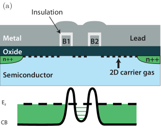
The general working principle of the planar quantum dot heterostructure closely resembles that of a MOSFET – in that the band structure of the semiconductor is manipulated electrostatically by local gate electrodes, which are separated electrically from the silicon underneath by an isolating layer. The electrodes control the flow of carriers in the device and shape the potential profile required for quantum dot formation. The lateral configuration of the electrodes determines the region where the potential can be manipulated, while the voltage applied to individual gate electrodes creates the electric field that can control the height of the potential. When the voltage applied to the gate electrodes is sufficient, the conduction band (CB) or valence band (VB) is pulled above or below the Fermi level so that states become available for transport, confining the carriers to a 2D carrier gas.
In order to measure conductance through the device, source and drain regions are created by doping and ohmic contacting. Implantation regions form source and drain reservoirs and can be ohmically contacted to measure conductance through the device. Figure 1 shows the ideal case of the resulting potential in the heterostructure profile, being two tunnel barriers and a quantum dot in the middle, for the applied voltages on the gate electrodes.
I.1 Fabrication strategy
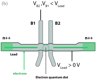
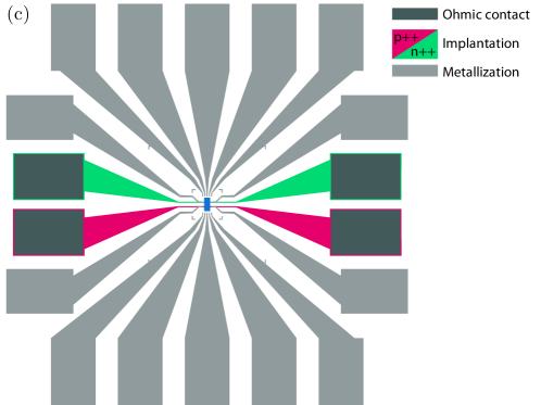
All devices in this work are made using the same fabrication strategy: first, the “big” structures, down to approximately 2 micron resolution, are defined at wafer scale using photolithography. This entails the oxidation of Si to form \ceSiO2, the formation of the implantation regions for the source and drain contacts, creation of the (high-quality) oxide, and the metallization of the electrodes which can be contacted later for measurement. Figure 1c shows the top view of the structures created in this process. Then, the smaller structures can be defined. Electron-beam lithography (EBL), followed by evaporation and lift-off is used to define the sub-micron gate electrodes. The device usually consists of more than one layer of electrodes, and therefore an insulating layer is needed for electrical separation of electrode layers. Dividing the fabrication process in two steps at different scale allows for rapid iteration of device configurations, which are otherwise limited by the speed at which the definition of gate electrodes with EBL takes place.
I.2 The ambipolar concept
The behavior of charge carriers in the valence and conduction-band is different, and both charge carriers have different properties. As an example, in bulk and at band-minimum, the longitudinal and transverse effective masses for transport of electrons are reported as , , while for holes the effective masses are , Van Zeghbroeck (2004), respectively, with the rest mass of the electron. Furthermore, the spin-orbit coupling for holes in Si is higher than for their counterparts in the conduction band, since the orbital angular momentum is non-zero. The criteria for quantum dot formation therefore also differ.
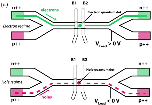
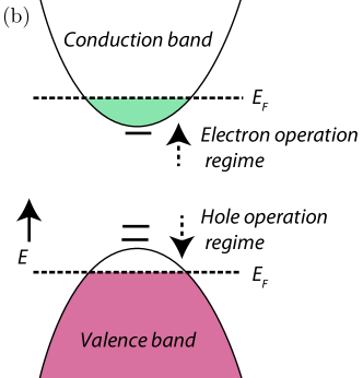
To explore this, ambipolar devices can be created where both holes and electrons can be used as charge carriers. Mueller et al. (2015); Betz et al. (2014); Jarillo-Herrero et al. (2004); Güttinger et al. (2009); Pfleiderer (1986); Chen et al. (2012) The planar quantum dot design is easily modified to create p- and n-type implantation regions at either end of the device. Which carrier is used to transport charge is controlled by gating the intrinsic silicon (Figure 2a). A negative potential on the gate will pull the VB above the Fermi level, making hole states available for transport. Conversely, applying a positive potential on the gate will push the CB below the Fermi level and make electron states available for transport. We call these modes of operation the hole and electron operation regime (Figure 2b). The ability to transport either electrons or holes in the same crystalline environment allows for the probing of states close to either the CB or VB of the semiconductor, while discounting fabricational variations that would otherwise exist when measuring these effects from one device to the next.
I.3 Heterostructure variations
In this work, we will encounter three variations on the basic heterostructure discussed in section I. The different designs attempt to address several issues, which we will discuss later.
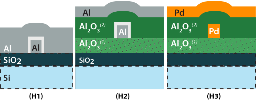
All heterostructures use \ceSiO2 as the first insulating layer. The first heterostructure (H1) uses Al as the material for gate electrodes, based on the recipe introduced by Angus et al.Angus et al. (2007) and can be seen in Figure 3(H1). Aluminum has the advantage that an insulating layer is easily created between the electrodes by thermal oxidation. In the second heterostructure (H2), a layer of \ceAl2O3 grown at is added between the \ceAl and the \ceSiO2, and a capping layer of \ceAl2O3 (not shown) is finally grown at . The third heterostructure (H3) substitutes the \ceAl for \cePd as the gate-electrode material, and maintains the inter- and capping-layer of \ceAl2O3.
II Layer synthesis techniques
For a well-defined electrochemical potential profile, it is essential to control the properties of the materials constituting a heterostructure. Here we will briefly touch on some aspects of these techniques, which we will relate in section III to how they might influence QD formation.
II.1 Physical vapor deposition
There are several methods of physical vapor deposition in common use today.
Firstly, thermal evaporation utilizes resistive heating of a crucible (typically made from W or Mo) filled with the material to be evaporated. For evaporation of metals, there are a few parameters of note. First, the rate of evaporation, controlled primarily by temperature, determines the grain size of the thin film. The difference in temperature between the evaporated material and the substrate determines the grain size of the polycrystalline film. The second aspect is the purity of the evaporated material. Since the evaporated material is situated in a thermally heated crucible, there is the possibility of contamination from the crucible material. For deposition pressures of the evaporated material can be considered to be in the ballistic regime.Lakhtakia and Messier (2005)
The second common technique, electron-beam evaporation, has several advantages in contrast to thermal evaporation, in that there is less danger of contamination by the crucible. Because for most materials the e-beam heats the sample locally, a small puddle is formed inside the target material. This puddle is thus only in contact with the same constituent material. Putting e-beam evaporation at a disadvantage however, is that X-rays are generated in the impact of the high-energy electrons with the target material. Possible damage to the substrate is therefore a concern. Grain size in this system is also controlled by the substrate temperature. Exploiting this, it has been shown for Al that cooling of the substrate can greatly improve the grain size of the thin film. Müller (2015) For typical evaporation rates of around 1-5 Å/s grain sizes of 15-40 nm have been reported for Pd Amin-Ahmadi et al. (2013), while for Al the grain sizes vary from 20-40 nm for the same range of ratesBordo and Rubahn (2012).
Thirdly, atomic layer deposition (ALD) is a technique independently discovered in the 60s in the Soviet Union and in the 70s in FinlandPuurunen (2014). It makes possible the controlled layer-by-layer growth of oxides, metals, fluorides, nitrides, sulfides, carbides, etc. ALD is a self-limiting process and is a subset of chemical vapor deposition. Its main advantages are the low temperatures at which the process can be used, precise control over film thickness, and conformal coverage of the resulting film. In this work ALD is used for the growth of \ceAl2O3.
In general two precursor gases are used, which react in two separate steps as described in reaction equations 1, LABEL:eq:ald_oxidize.
| (1) | |||
The simplified reaction equations as given in equation LABEL:eq:ald_oxidize bely some more complicated reactions that can take place, as the use of \ceH2O as a precursor gas has been shown to create hydrogen as a reaction by-product in the ALD-cycle. Dingemans et al. (2010) This causes ALD-grown \ceAl2O3 to have hydrogen content at 2-3 at.%. Experiments with deuterated water as a precursor show deuterium diffusing from the \ceAl2O3 film toward the Si interface at annealing temperatures of , where dangling bonds are passivated and lead to a lower density of interface states .
The growth temperature of the \ceAl2O3 determines the density of the oxide. The hydrogen content will be shown to have an important consequence later on in section IV.
II.2 \ceSiO2 growth
The growth of \ceSiO2 can be accomplished by simply introducing an oxidant to silicon at high temperature. The oxidant diffuses through the silicon and oxidizes the silicon from the top up to the desired depth.
Wet oxidation is generally used to create thick, but qualitatively poor, oxides at a rate of 400 nm/h at and takes place by introducing \ceH2O as the oxidant. Dry oxidation occurs in \ceO2-containing ambient and oxidizes the silicon at rates far slower than for wet oxidation ( 100 nm/hr). The latter process yields a denser oxide with fewer defects and higher breakthrough voltages.
Oxygen, introduced at high temperature, will oxidize the top layer of the silicon first. The newly created oxide takes up more volume than was occupied by silicon before oxidation. This decrease in density allows more oxygen to penetrate deeper into the silicon, and oxidizes at the newly formed Si/\ceSiO2 interface. The process continues and the Si/\ceSiO2 oxidation front progresses further down into the substrate. Because of the increase in volume, taking place at , the silicon lattice will be uniformly stressed by the \ceSiO2. Thorbeck and Zimmerman (2015)
The Deal-Grove model describes the oxidation reaction as occurring at the Si/\ceSiO2 oxidation front. It describes the diffusion of the oxidant through the already formed oxide in terms of concentration differences, for which the model assumes steady-state conditions. Discrepancies of the Deal-Grove model for thin oxides have led to new insights and it has been shown that a more complete model involving Si emission from the surface describes thin oxides better. Kageshima, Shiraishi, and Uematsu (1999); Uematsu, Kageshima, and Shiraishi (2002a) The quality of the oxide can be further improved by the addition of chlorine-containing gas during oxidation. The reduction of atomic silicon emission from the silicon by the chlorine is most likely responsible for this. Uematsu, Kageshima, and Shiraishi (2002b)
It is important to note that the oxidation process is not isotropic. Should thermal oxidation start at a surface that is made atomically flat; that flatness would not propagate to the Si/\ceSiO2 interface under normal conditions. Furthermore the conditions for oxidation lead to a wide array of interface morphologies Yamabe et al. (2009, 2001); Ravindra and Narayan (1987). One possible solution for this might be a new technique using a microwave-excited high-density plasma with low electron temperatureOhmi, Hirayama, and Teramoto (2006); Aratani et al. (2008). The free radicals created in this process have been shown to lead to a more abrupt \ceSi/\ceSiO2 interface and to preserve the atomically flat nature of as-prepared wafers.Kuroda et al. (2009) The nature of this interface has not been fully explored yet, save for theoretical studies that suggest a phase of atomically flat, and stable \ceSiO2 can exist.Tsetseris and Pantelides (2006)
III Defects in quantum dot heterostructures
As mentioned previously, the fragile nature of quantum states means that many effects which do not affect mesoscopic devices, play a big role in nanodevices.
We identify roughly three categories for heterostructures. These categories will serve as rough guides to determine where effects occur in heterostructures, which in turn might influence design considerations. The first category consists of the inherent material properties of the constituents of the heterostructure. These are mainly determined by the initial growth process, but can also be influenced during processing. The second category concerns interfaces, which can manifest a-priori unexpected phenomena. This is a broad and active area of research unto itself which has garnered interest due to its fundamental physical concepts involving e.g. the breaking of symmetries.
The third are morphological effects. We can think e.g. of the morphology of the gate layout intended to form intentional quantum dots. However, there are many more unforeseen morphological effects which can occur and must be considered.
We will look at these categories, guided by the three main heterostructures used in this work, as introduced in section I.3.
III.1 Materials
We will start by examining the basic building blocks of heterostructures, their materials. It is the intrinsic material properties of silicon that make it a highly valued candidate for quantum computing. Let us briefly review what material properties influence the formation of our quantum dots.
III.1.1 High-quality oxide
The creation of an inversion layer in silicon requires the application of a voltage to electrodes typically separated from the silicon by only a few tens of nanometers of oxide. The electric fields over this short distance are thus large, and on the order of MV/cm. The oxide should be able to withstand these high voltages and avoid pinhole defects that occur when reaching the so-called breakthrough voltage.
For all three heterostructures in this work, the process for creating a high-quality oxide is the same. The addition of chlorine during growth improves our breakthrough voltage of the oxide. Without it, significantly smaller breakthrough voltages were observed after dopant activation in a rapid thermal annealing process (RTA).
III.1.2 Damage incurred by processing
However perfect the material grown during a process step, it is possible that high-energy processes during further processing of the heterostructure cause damage. The thermal budget is a common indicator used to signify the maximum allowed thermal load before a device will be too damaged. Process damage manifesting as an increase in defect density is also known to occur when using electron-beam evaporationSchiele, Hahn, and Terheiden (2011). This is most likely caused by the X-rays generated during the evaporation process. Another defect known to be generated by high-energy radiation is the E′ defect in \ceSiO2Messina et al. (2009).
Thus far, little research has been done on the damage electron beam lithography can cause in heterostructures. It is however reasonable to expect that the high-energy electrons (as high as 100 keV) do interact with the materials in the heterostructure. It was shown recently that shallow defects can result from exposure to EBL. The resultant degraded mobility could be recovered to a great degree by annealing in forming gas (5% \ceH2, ) for 25 min.Kim, Tyryshkin, and Lyon (2017)
It is not a-priori clear if a high-energy beam or a low-energy beam would be preferable, since scattering mechanisms in the entire heterostructure determine where the majority of energy of the beam is absorbed. Several models for this type of problem, based on energy deposition in (amorphous) solids have been suggested.Kobetich and Katz (1968); Kanaya and Okayama (1972) Low-energy patterning (up to a few keV) on thin layers of resist could alleviate this problem.
All heterostructures in this work have been exposed to EBL processes at energies of typically 20 to 28 keV.
III.1.3 Dewetting
Dewetting is the breaking of continuity of an initially continuous film caused by differences in free surface energy at liquid-liquid or solid-liquid interfaces. In our case the interface consists of either Al/\ceSiO2, Al/\ceAl2O3 or Pd/\ceAl2O3. At elevated temperatures thin films of metal, while still below their melting point, can become mobile. Dewetting becomes energetically favourable under the right circumstances: temperature, granularity of the film, free surface energy at the Al/ and vacuum/Al interface. The process is illustrated in Figure 4.
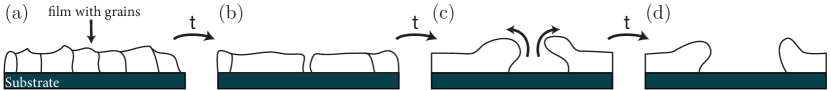
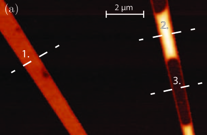
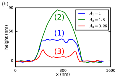
Figure 5a shows dewetting behavior as observed in one of our samples after annealing. The left Al electrode, labeled (1) still has its as-deposited height of 36 nm. The right electrode shows clear signs of dewetting. At (2) the height has increased from 36 nm as-deposited to a maximum of roughly 90 nm. The material for this height increase has been moved from (3) to (2). The areas underneath curves taken at (1), (2), and (3) are normalized to . We see that , i.e the material “missing” from (3) has moved to (2), and thus the sum equals twice the original. At the interface region between (2) and (3) the convex/concave shape is reminiscent of the classical meniscus in e.g. water, indicating energy minimization caused by surface tension. Thompson (2012) This can also be observed on both sides of the electrode at (3).
III.1.4 Properties of Al at elevated temperatures
At elevated temperature other effects concerning Al can arise. It has been reported that \ceAlO_x hillocks are created when exposing Al on \ceAl2O3 to a high temperature step of Dutta et al. (2012); Gardner and Flinn (1988). The spiking of Al through 1.5 nm of \ceSiO2 has also been reported for annealing temperature of . Bierhals, Aberle, and Hezel (1998) Furthermore, void formation by stress release of Al at temperatures of 300 to has been reported. Hinode, Asano, and Homma (1989)
III.2 Interfaces
To fully characterize the heterostructure, the interfaces between the constituent materials have to be considered. The physics of interfaces is a broad field with many interesting topics. There are many examples where the discontinuity at the interface between two materials can lead to interesting physics, such as Rashba-type spin-orbit couplingBychkov and Rashba (1984), or a finite conductivity at the interface between the two insulators \ceLaAlO/\ceSrTiO3Ohtomo and Hwang (2004).
The three heterostructures studied in this work have many interfaces, starting from the Si/\ceSiO2 to the metal/oxide interface. Naturally, the addition of an extra layer of material also introduces an additional interface where effects might occur.
III.2.1 The \ceSi/\ceSiO2 interface
The first interface we will consider is the \ceSi/\ceSiO2 interface, where a transition from crystalline Si to an amorphous matrix of \ceSiO2 breaks continuity and translational symmetry. At an atomic scale, the crystalline Si and amorphous \ceSiO2 are incommensurable, save for some theorized phases of \ceSiO2 that would give an abrupt interface.Pantelides et al. (2001)
The Si/\ceSiO2 interface has been extensively studied in the context of MOSFET technology. The focus here has primarily been on defects. One of the most studied defects at this interface is the paramagnetic centerNishi, Tanaka, and Ohwada (1972); Thoan et al. (2011); Mishima and Lenahan (2000) which is linked to surface charges, decreased mobility, and the negative-bias temperature instability (NBTI) effectSchroder and Babcock (2003); Campbell et al. (2007). For quantum computation, centers have been used in coherent manipulation of spin-dependent charge-carrier recombination of phosphorus donorsStegner et al. (2006). Additionally, the coherence times of these phosphorous donors have been shown to be adversely affected in proximity to \ceP_b centers.Paik et al. (2010) Defects at the interface have also been associated with random telegraph signals at low temperatures and characterized by means of single-electron spin resonance Xiao, Martin, and Jiang (2003); Xiao et al. (2004) and magnetic-field dependent measurementsPrati et al. (2006).
\ceP_b centers, E′ centers
It is useful to categorize traps of influence at the Si/\ceSiO2 oxide interface by distance to the interface. We can discern, in order of increasing distance, interface traps, border traps, and oxide traps (Figure 6). The two most prevalent defects are \ceP_b centers, which is an interface trap, and E′ centers, which are typically classified as border traps or oxide traps.
The center is in essence a Si atom with a dangling bond that has formed due to the incommensurability of the crystalline Si and the amorphous . Two types of \ceP_b center can be further distinguished for Si (100). The center is backbonded to two Si atoms and one oxygen atom, while the center is backbonded to three Si atoms. The corresponding atomic configurations can be seen in Figure 6. For the center, the density of interface states in the gap has been measured in capacitance-voltage (CV) and electron paramagnetic resonance measurements (EPR) to be amphoteric in nature with its maxima at and eV above the valence band Ragnarsson and Lundgren (2000).
The second common defect is the E′ center. This defect in \ceSiO2 is a binary structure: an oxygen vacancy with unpaired Si spin on one side, \ceO3# Si and a stripped positively charged \ce^+Si# O3 on the other side. The E′ center is a common occurrence in thermal oxide and is a possible source of oxide fixed-charge.Caplan et al. (1979) It is characterized as a border trap, situated farther in the oxide than the \ceP_b center.
The presence of these defects plays a significant part in the formation of quantum dots, and can prevent quantum dot formation distorting the confinement potential and providing additional levels for tunneling. Spruijtenburg et al. (2013) Elimination of defects, such as the center, is commonly achieved through chemical passivation by introducing hydrogen in an annealing process. This process reduces the dangling bond spatial density from order to and improves numerous parameters related to MOSFET-like transistor operation. It has also been shown to improve parameters related to quantum dot formation Cartier, Stathis, and Buchanan (1993); Angus et al. (2007).
In order to create quantum dots reliably, it is thus necessary to perform this annealing step. For the heterostructures H1-H3 used in this work, the following applies:
-
•
For H1, there is no passivation/annealing step. Annealing using a standard forming gas anneal of \ceH2/\ceN2 in this architecture was not possible due to dewetting, which is described in detail in section III.1.3. The lack of annealing leads to single-hole tunneling through charge defects located underneath barriers in all cases Spruijtenburg et al. (2013).
-
•
Heterostructure H2 introduces ALD-grown \ceAl2O3 layers. The covering \ceAl2O3 layer allows for annealing without dewetting, because it caps the entire structure and contains hydrogen as described in section II. This process is shown to reduce charge defects to a substantial degree Spruijtenburg et al. (2016); Angus et al. (2007).
-
•
Heterostructure H3 should show no appreciable difference at the Si/\ceSiO2 interface from H2, since only the gate-electrode material has been altered. There is the outside chance that the presence of Al improves annealing characteristics, in a process commonly known as alnealing.
[]
 \sidesubfloat[]

Atomically flat/rough silicon
As discussed in section II.2, the interface between silicon and \ceSiO2 is not expected to be atomically flat but rather have a finite roughness. This is further exacerbated by the etching of silicon by BHF before high-quality oxide growth, which is known to roughen the surface and leave Si{110} faceted nanoscale hillocks on the Si surface.Aldinger and Hines (2012) For all architectures in this work, this interface has been prepared in the same manner, and is expected not to be atomically flat.
The roughness, with its characteristic length scale, causes the electrochemical potential to fluctuate. If the length scale of the carrier wave function is comparable to the length scale of the roughness, this could lead to effects such as Anderson localization, a strong decrease in current in the deviceSvizhenko, Leu, and Cho (2007), or unintentional spinflips Fleetwood, Pantelides, and Schrimpf (2008). Optimizing how abrupt the Si/\ceSiO2 interface is, would be a good candidate for improvement of quantum dot properties. As a means for spin-manipulation, the use of atomic steps has also been suggested.
Obtaining atomically flat silicon is possible by using using low-energy ion sputtering and a subsequent temperature step at . Kim et al. (2003) Another method shown to work is to anneal the Si in ultrapure argon at Kuroda et al. (2009). The surface is heated by Ar bombardment and recrystallizes in the lowest energy state. The key parameter in this process is the amount of trace oxygen, which in other cases etches the silicon and induces roughness. Among the reported improvements of this atomically flat Si have been the noise characteristics of MOSFET structures. Kuroda et al. (2009) Chemical means have also been attempted by etching in aqueous \ceNH4F (40 %), although atomics steps were not observed.Aldinger and Hines (2012)
III.2.2 The \ceSiO2/\ceAl2O3 interface - fixed charge in \ceAl2O3
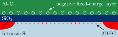
The negative fixed charge in as-grown \ceAl2O3 has been measured to be Dingemans and Kessels (2012) . Subsequent annealing of this thermally grown layer increased to a maximum of , depending on the annealing temperature and ALD growth technique.
It has been proposed that the negative fixed charge is caused by a very thin interfacial layer that is off-stoichiometricSimon et al. (2015) and can be controlled by growing a preceding layer of \ceHfO2 before the growth of the \ceAl2O3. Figure 7 shows schematically the location of the proposed fixed charge .
Samples without gate structures were grown with \ceAl2O3 layer and another layer of grown at , and annealed at in \ceH2. These samples showed hole conduction on the order of at . Would there be no fixed charge present, at all the charge carriers in the intrinsic silicon are frozen out and no conduction would be observed.
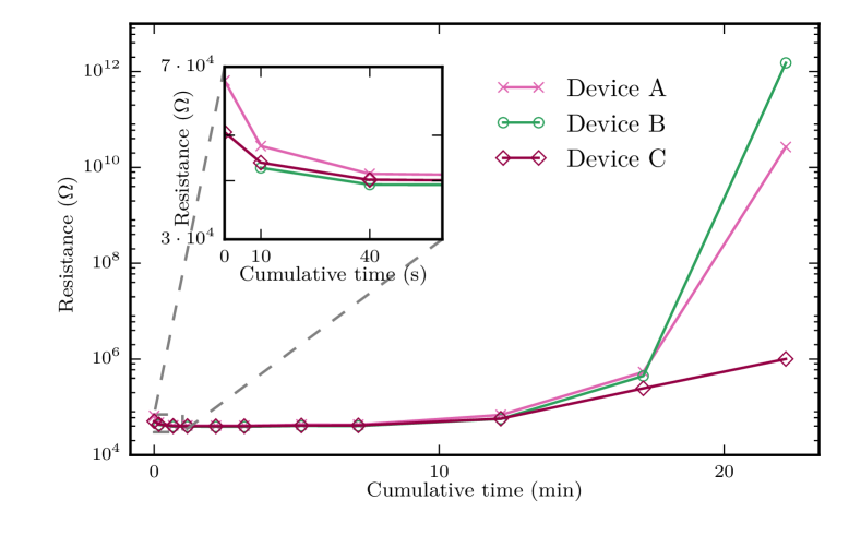
An interesting effect on the fixed charge was observed when exposing the samples to ozone in a UV-ozone reactor. Figure 7 shows the behavior of the resistance of three devices with no gate electrodes deposited and only had the layers of \ceAl2O3 grown. This resistance is shown as a function of cumulative time processed in an UV-ozone reactor. Startup transient effects such as the heating up of the mercury lamp in this reactor have not been taken into account. An initial increase of conduction was observed when processing the samples in a UV-ozone reactor. This is proposed to be due to further population of the charge traps by carriers excited over the band gap by the UV photons. After this initial decrease in resistance it is seen that after approximately 10 minutes the resistance increases again. The latter can be explained by the oxidative effect of the ozone, which fills the oxide vacancies in the \ceAl2O3.
Recently we have used the fixed charge in the \ceAl2O3 to realize depletion-mode quantum dots in intrinsic siliconAmitonov et al. (2018).
[]
[]
III.2.3 The \ceSiO2/Metal or \ceAl2O3/Metal interface
To create the oxide/metal interface, metal is deposited by thermal or e-beam evaporation after lithography. In this process, the hot metal vapor is deposited on the colder substrate and interacts with said substrate. Ideally, the metal bonds to the substrate and adheres well enough to survive further process steps, such as lift-off. Should adhesion be a problem for the materials involved, an intermediate adhesion layer of a different material can be grown. These sticking layers are generally made of small radius atoms, such as Ti.
Our MOS heterostructures are always dealing with metal/oxide interfaces. Before we continue let us briefly consider the stability of phases in compounds consisting of more than two constituent atoms. In our case we are dealing with the oxide and the metal. For the \ceSiO2/Al interface e.g. we are dealing with the three atomic species Si, Al, and O. Given these three atomic species, the most stable compound is dictated by their Gibbs free energies. The energies of the phases of various materials can be read out from an Ellingham diagram, which tabulates the Gibbs free energy versus temperature.
Given the mixture of Si, Al, and O for H1 at the metal/oxide interface, and the Gibbs free energies of the compounds \ceSiO2 ( = ) and \ceAl2O3 ( = ) at , we expect that the most stable compound is the \ceAl2O3. This implies that at the interface the Al is reduced by O, which is consumed from the \ceSiO2 layer, leaving elemental Si and \ceAl2O3.
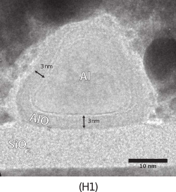
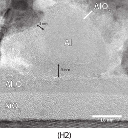
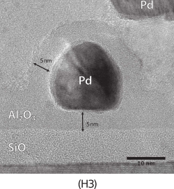
To explore the interfaces, we will now evaluate all three heterostructures on the basis of transmission electron microscopy (TEM) studies in Fig. 8b.
First, let us discuss H1, with its \ceSiO2/Al interface, shown in Figure 8a. An oxide layer can be seen surrounding the crystalline Al core. Given that the electrode has undergone the standard oxidation in ambient at for 10 minutes, the oxide layer is indeed expected. However, would this step have been the only oxidation process, one would expect more oxide formation at parts of the electrode exposed to ambient. The width of this interfacial layer is also too broad to have originated purely from oxidation from the side. The thickness of the interfacial \ceAl2O3 layer is determined to be .
The interface layer extends beyond the imaginary line of the \ceSiO2 plane. This indicates that the Al has “eaten” into the \ceSiO2 layer. Previous studies on the phase formed at this interface have concluded that a mixture of and phases are likely formed. These are less dense and have more “open” structures than the most stable \ceα-Al2O3 Roberts and Dobson (1981).
Given that the formation of this interfacial layer could contain elemental Si and an undefined phase of \ceAl2O3, it would be beneficial to eliminate the interfacial layer. Heterostructure 2 introduces an intermediate ALD-grown \ceAl2O3 layer, changing the constituents of the oxide/metal interface as compared to heterostructure 1. It would be expected that the interface layer is reduced because the \ceAl2O3 is stable and there is no reason for the Al to be oxidized. Figure 8b shows a TEM image of this heterostructure. As compared to heterostructure 1 the same surrounding oxide layer is observed. However, the interfacial layer has instead increased to . It could be that the \ceAl2O3 underlayer is able to transport oxygen efficiently, or the electron affinity of Al allows for easier dissociation than for \ceSiO2, combined with a diffusion process.
The third and final heterostructure supplants Al for Pd, and utilizes the ALD-grown \ceAl2O3 intermediate layer. It is immediately visible in Figure 8c that there is no more surrounding oxide layer, perhaps because Pd knows no native oxide. The contrast of the Pd with the surrounding \ceAl2O3 indicates that there is a negligible transition layer.
III.3 Morphology
In the end, quantum dot formation will be determined by the shape, size, and layout of the gate electrodes. Therefore, as a final category we will discuss the morphology of the heterostructure. We will discuss effects related to the morphology of the heterostructure. The shape of the structures as they interact with temperature and electric field, change the potential landscape that influences quantum dot formation.
III.3.1 Thermally induced non-uniform strain
Strain is an important parameter in MOSFETs and has been used to manipulate mobility for better performance in e.g. finFETsNeizvestnyi and Gridchin (2009); Horstmann et al. (2005). Recently it has come to light that the morphology of the gate structure, together with differing thermal expansion coefficients, can lead to local strain in the heterostructure. Thorbeck and Zimmerman (2015)
The argument for this is as follows. Measurement of quantum dot devices is nearly always done at cryogenic temperatures. The expansion coefficient of each material is different, and thus each material contracts at a different rate. The resulting situation for a simple case of a metal gate electrode on a semiconductor material is sketched in Figure 1 of Ref. Thorbeck and Zimmerman (2015). At room temperature the materials can be considered nearly stress free, however when cooling down to cryogenic temperatures the metal will contract more than the substrate, causing compressive strain in the substrate. The strain modulates the CB/VB on both ends of the metal gate, effecting a change in potential at these locations. The created potential confines carriers, and an unwanted quantum dot is created. Mitigating this effect, should one chose to, can be achieved by choosing metals with an expansion coefficient comparable to the substrate. In the case of Si, poly-Si would be ideal. Alternatively, the distance to the substrate by adding more layers in between electrode and substrate could be increased. This would allow more relaxation of stress.
Let us again evaluate the consequences of this effect in our three heterostructures. Heterostructure 1 utilizes Al as a gate electrode material, which has one of the biggest thermal expansion coefficients. It is separated from the Si by only 8 nm of \ceSiO2. One can thus expect that the effect will be biggest in this heterostructure.
Because the gate electrode layer is separated by an additional \ceAl2O3 layer in heterostructure 2, it is expected that strain is relieved more before reaching the Si. As discussed, mitigating the effect can also be accomplished by changing the electrode material. Pd has an expansion coefficient nearly twice as small as Al. It is expected that among the three heterostructures, H3 has the least local strain, firstly because the gate-electrode/Si separation increases by the \ceAl2O3 layer and secondly it uses Pd as an electrode material.
III.3.2 Unintentional dielectric dots
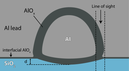
Another morphology effect, concerns the interaction with the electric field, and is also related to the formation of unintentional quantum dots.
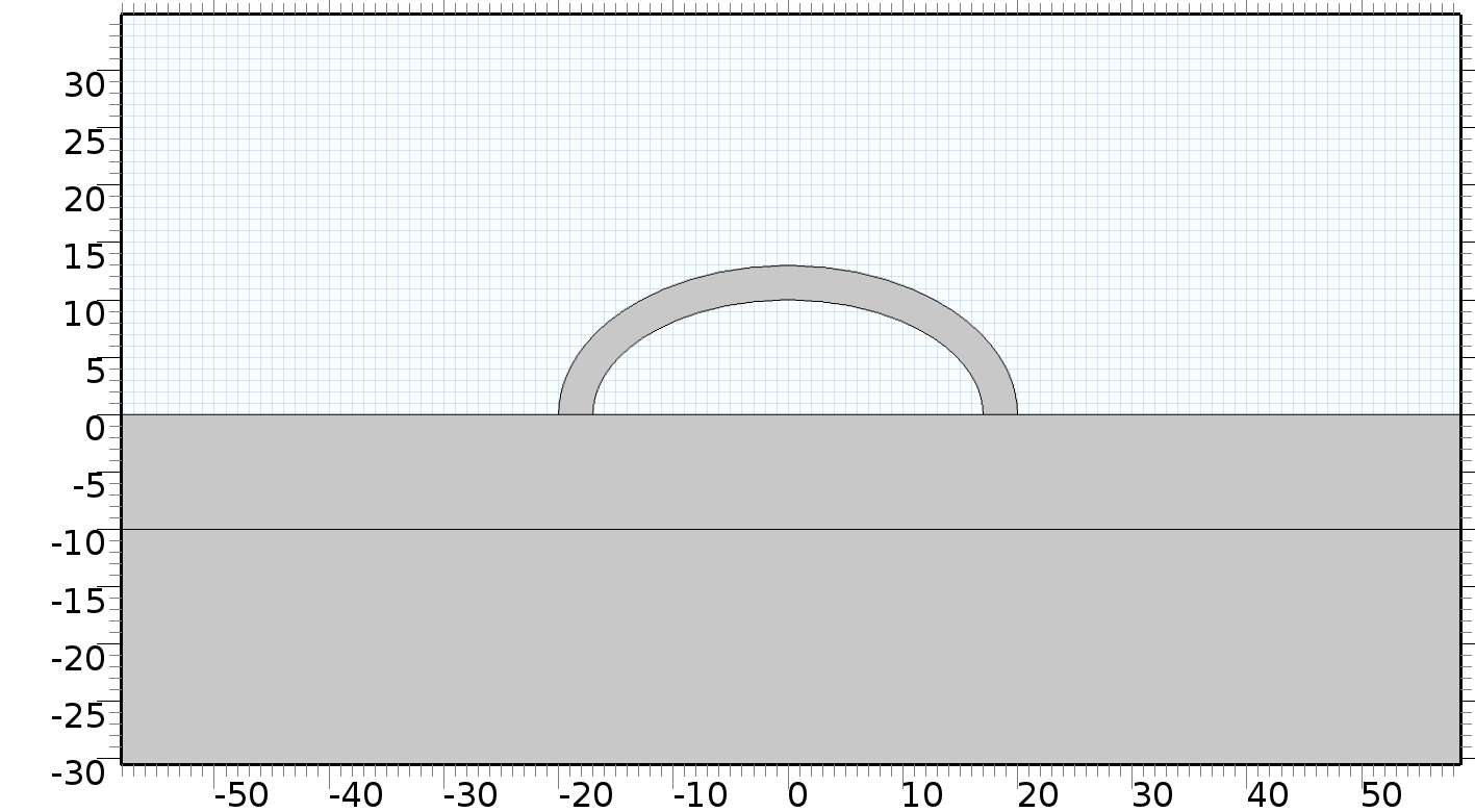
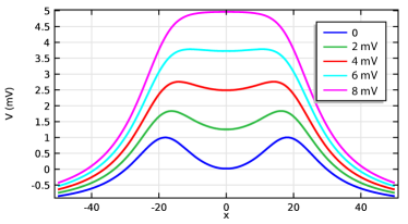
In all heterostructures the first electrode layer is separated by a dielectric from the second electrode layer. This has the consequence that, when applying a voltage to the second covering electrode layer, the electric field gradient is smaller because it has to traverse more dielectric. This results in a potential that is slightly different at the sides of the first layer electrode. Figure 9 depicts this schematically with the lead gate having a “line of sight” to the semiconductor material. Along this line of sight the amount of dielectric material is larger. A simple simulation of this effect is shown in Figure 10. Here the resulting potential is shown (1 nm below the \ceSiO2 dielectric) as a function of difference in voltage on the lead and barrier gate. The resulting potential deviates from the ideal tunnel barrier potential on the order of mV when the voltage on the lead and barrier electrode is equal. This could lead to the formation of an unintentional quantum dot.
[]
 \sidesubfloat[]
III.3.3 Grains in aluminum
[]
 \sidesubfloat[]
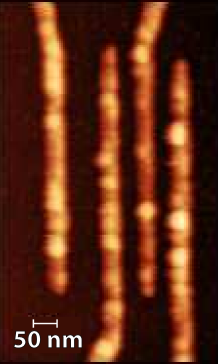
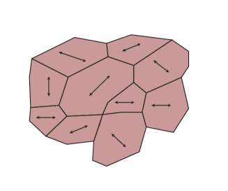
As discussed in section II, when evaporating thin films of metal an important parameter is the grain size of the resulting polycrystalline film. Especially when, in evaporating laterally constricted electrodes, the grain size becomes comparable to the width of the defined electrodes. This will result in an edge of the film which is rough along the line definition. An example of this for Al is given in Figure 11. As in all other mechanisms described previously, the resulting potential will thus also be rough. It has been shown that roughness can lead to localization of a quantum dot Voisin et al. (2014). Another mechanism which could be conceived is that the differently oriented strain in separate grains could modulate the electrochemical potential via the thermally induced strain mechanism described previously. This is schematically depicted in Figure 11.
IV The annealing process
Elimination and passivation of defects at the Si/\ceSiO2 interface is commonly achieved by annealing in a \ceH2/\ceN2 environment.
The passivation process for \ceP_b centers is governed, in the naive case, by
with associated activation energies and Stesmans (2000). The rates of passivation and depassivation and are determined by temperature, through the Arrhenius expression . The rates of the passivation and depassivation reaction lead to an equilibrium of the defect density. There is thus an optimum temperature at which the passivation process is most effective.
In this work we use ALD-grown \ceAl2O3 to passivate our heterostructure. The process is done in two steps, with the growth of \ceAl2O3 taking place at , and a separate annealing step done at .
The existence of hydrogen in ALD-grown oxide was shown through the use of deuterated water as a precursor.Dingemans et al. (2010) Studying the depth profile of the deuterium, it was determined that the concentration in the \ceAl2O3 was reduced, while the content of deuterium in the \ceSiO2 and at the Si/\ceSiO2 interface showed a sharp increase, indicating the deuterium was being consumed in a passivation process.
The degree of passivation is determined by two factors. The first is the oxide growth temperature , which determines the density of the oxide, and its hydrogen content. The optimum for passivation is reached when the effusion of hydrogen, controlled by the density of the oxide, is minimized, while the amount of hydrogen present is kept sufficient to passivate all dangling bonds in the annealing step that follows.
The second factor controlling the degree of passivation is the annealing temperature . Besides determining the final equilibrium defect density, also determines how quickly this is reached. The best annealing temperature was previously determined to be Dingemans et al. (2012). Using this process, defect densities as low as have been reported.Dingemans and Kessels (2015) The activation energy for passivation has been shown for ALD-grown \ceAl2O3 to be = .
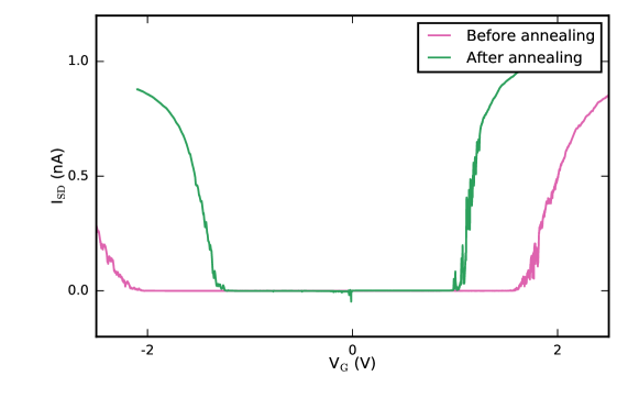
The ambipolar design of our heterostructures allows us to illustrate this process and its effects quite nicely in the effects on the threshold voltages . Figure 12 shows the current-voltage characteristics of a device with a heterostructure 2 design, with a single Al accumulation gate. The sample was measured once, before covering it in ALD-grown \ceAl2O3 with . It was then annealed at in Ar ambient for 45 minutes, and measured again.
It can be seen that is reduced for both the hole and electron-operation regime after annealing. The absolute voltage decrease of between the hole and electron-regime is related to the decrease in \ceP_b centers, which are amphoteric defects capable of storing both negative and positive charge. The layer of \ceP_b centers can thus be seen as an extra capacitor in series with the dielectric.
V Discussion and conclusion
We have reviewed the many effects that can occur in heterostructures relating to quantum dot formation, and have identified effects pertaining to three categories: Materials, interfaces and morphology.
The planar quantum dot architecture first introduced by Angus et al.Angus et al. (2007) (H1) has been very successful. Lim et al. (2009); Veldhorst et al. (2015) Further optimization and expansion of this approach therefore bodes very well for the future. We have identified several areas where improvements can be made.
Firstly, we have observed that the ability to passivate defects at the Si/\ceSiO2 interface through annealing hinges primarily on the prevention of dewetting at higher temperatures. In this way, introduction of an ALD-grown \ceAl2O3 layer (H2) improves upon the Angus design. This kills two birds with one stone as it prevents dewetting, and enables the annealing of defects using (at least) the hydrogen present inside the grown film.
Unexpectedly however, an increase of the oxide layer directly beneath the Al electrode is observed. We postulate this might be due to an enhanced solubility of Al as compared to Si, or an oxygen diffusion process, which would be more efficient in \ceAl2O3. The ability to anneal these devices now allows very well defined quantum dots up to 180 nm in lengthSpruijtenburg et al. (2016).
Supplanting Al by Pd as the electrode material in H3 prevents the formation of an interfacial layer between the Pd and the \ceAl2O3, as can been seen in TEM images. Pd would reduce temperature-induced strain, since its expansion coefficient is less than that of Al. It is unclear how and if the polycrystalline nature of Pd differs from Al, which could play a role in strain-related unintentional quantum dots. We have measured many devices with Pd gates, resulting in reproducible low-disorder quantum dots Brauns et al. (2017).
A remaining issue is the fixed-charge present in the ALD-grown \ceAl2O3. This can be a nuisance for quantum dot formation, since it induces a 2DHG, even in areas where no electrodes are present. It can however also be used in creating depletion dots Amitonov et al. (2018).
Further optimization might include material such as poly-Si or TiN as an electrode material, which are amorphous materials, and therefore either have a non-uniform or reduced temperature-induced strain. The creation of an abrupt, atomically flat Si/\ceSiO2 interface could also improve the reliability of quantum dot formation.
Acknowledgements We acknowledge Alexey Kovalgin and Tom Aarnink for comments on the manuscript and their technical expertise with regards to atomic layer deposition. This work is part of the research program “Atomic physics in the solid state” with project number 14167, which is (partly) financed by the Netherlands Organisation for Scientific Research (NWO).
References
- Fowler et al. (2012) A. G. Fowler, M. Mariantoni, J. M. Martinis, and A. N. Cleland, Physical Review A - Atomic, Molecular, and Optical Physics 86 (2012), 10.1103/PhysRevA.86.032324.
- Chen et al. (2012) J. C. H. Chen, D. Q. Wang, O. Klochan, A. P. Micolich, K. Das Gupta, F. Sfigakis, D. A. Ritchie, D. Reuter, A. D. Wieck, and A. R. Hamilton, Applied Physics Letters 100, 2012 (2012).
- Borselli et al. (2011) M. G. Borselli, K. Eng, E. T. Croke, B. M. Maune, B. Huang, R. S. Ross, A. A. Kiselev, P. W. Deelman, I. Alvarado-Rodriguez, A. E. Schmitz, M. Sokolich, K. S. Holabird, T. M. Hazard, M. F. Gyure, and A. T. Hunter, Applied Physics Letters 99, 063109 (2011).
- Katsaros et al. (2010) G. Katsaros, P. Spathis, M. Stoffel, F. Fournel, M. Mongillo, V. Bouchiat, F. Lefloch, A. Rastelli, O. G. Schmidt, and S. De Franceschi, Nature Nanotechnology 5, 458 (2010).
- Zwanenburg et al. (2009) F. A. Zwanenburg, C. E. W. M. van Rijmenam, Y. Fang, C. M. Lieber, and L. P. Kouwenhoven, Nano Letters 9, 1071 (2009).
- Brauns et al. (2016) M. Brauns, J. Ridderbos, A. Li, W. G. van der Wiel, E. P. A. M. Bakkers, and F. A. Zwanenburg, Applied Physics Letters 109, 143113 (2016).
- Horibe, Kodera, and Oda (2015) K. Horibe, T. Kodera, and S. Oda, Applied Physics Letters 106, 1 (2015).
- Lim et al. (2009) W. H. Lim, F. A. Zwanenburg, H. Huebl, M. Möttönen, K. W. Chan, A. Morello, and A. S. Dzurak, Applied Physics Letters 95, 242102 (2009).
- Zwanenburg et al. (2013) F. A. Zwanenburg, A. S. Dzurak, A. Morello, M. Y. Simmons, L. C. L. Hollenberg, G. Klimeck, S. Rogge, S. N. Coppersmith, and M. A. Eriksson, Reviews of Modern Physics 85, 961 (2013).
- de Sousa and Das Sarma (2003) R. de Sousa and S. Das Sarma, Physical Review B 68, 115322 (2003).
- Kuhlmann et al. (2013) A. V. Kuhlmann, J. Houel, A. Ludwig, L. Greuter, D. Reuter, A. D. Wieck, M. Poggio, and R. J. Warburton, Nature Physics 9, 570 (2013).
- Rashidi et al. (2016) M. Rashidi, J. A. J. Burgess, M. Taucer, R. Achal, J. L. Pitters, S. Loth, and R. A. Wolkow, Nature Communications 7, 13258 (2016).
- Laucht et al. (2016) A. Laucht, R. Kalra, S. Simmons, J. P. Dehollain, J. T. Muhonen, F. A. Mohiyaddin, S. Freer, F. E. Hudson, K. M. Itoh, D. N. Jamieson, J. C. McCallum, A. S. Dzurak, and A. Morello, Nature Nanotechnology 12, 61 (2016).
- Shi et al. (2012) Z. Shi, C. B. Simmons, J. R. Prance, J. K. Gamble, T. S. Koh, Y.-P. Shim, X. Hu, D. E. Savage, M. G. Lagally, M. A. Eriksson, M. Friesen, and S. N. Coppersmith, Physical Review Letters 108, 140503 (2012).
- Zimmerman et al. (2008) N. M. Zimmerman, W. H. Huber, B. Simonds, E. Hourdakis, A. Fujiwara, Y. Ono, Y. Takahashi, H. Inokawa, M. Furlan, and M. W. Keller, Journal of Applied Physics 104 (2008), 10.1063/1.2949700.
- Stewart and Zimmerman (2016) M. Stewart and N. Zimmerman, Applied Sciences 6, 187 (2016).
- Greenland et al. (2010) P. T. Greenland, S. A. Lynch, A. F. G. van der Meer, B. N. Murdin, C. R. Pidgeon, B. Redlich, N. Q. Vinh, and G. Aeppli, Nature 465, 1057 (2010).
- Steger et al. (2012) M. Steger, K. Saeedi, M. L. W. Thewalt, J. J. L. Morton, H. Riemann, N. V. Abrosimov, P. Becker, and H.-J. Pohl, Science 336, 1280 (2012).
- Dohnalová, Gregorkiewicz, and Kůsová (2014) K. Dohnalová, T. Gregorkiewicz, and K. Kůsová, Journal of Physics: Condensed Matter 26, 173201 (2014).
- Amitonov et al. (2018) S. V. Amitonov, P. C. Spruijtenburg, M. W. S. Vervoort, W. G. van der Wiel, and F. A. Zwanenburg, Applied Physics Letters 112, 023102 (2018).
- Brauns et al. (2017) M. Brauns, S. V. Amitonov, P.-C. Spruijtenburg, and F. A. Zwanenburg, arXiv:1709.07699 [cond-mat] (2017), arXiv: 1709.07699.
- Van Zeghbroeck (2004) B. Van Zeghbroeck, Colorado University (2004).
- Mueller et al. (2015) F. Mueller, G. Konstantaras, P. C. Spruijtenburg, W. G. van der Wiel, and F. a. Zwanenburg, Nano Letters 15, 5336 (2015).
- Betz et al. (2014) A. C. Betz, M. F. Gonzalez-Zalba, G. Podd, and A. J. Ferguson, Applied Physics Letters 105, 153113 (2014).
- Jarillo-Herrero et al. (2004) P. Jarillo-Herrero, S. Sapmaz, C. Dekker, L. P. Kouwenhoven, and H. S. J. Van Der Zant, Nature 429, 389 (2004).
- Güttinger et al. (2009) J. Güttinger, C. Stampfer, F. Libisch, T. Frey, J. Burgdörfer, T. Ihn, and K. Ensslin, Physical Review Letters 103, 1 (2009).
- Pfleiderer (1986) H. Pfleiderer, IEEE Transactions on Electron Devices 33, 145 (1986).
- Angus et al. (2007) S. J. Angus, A. J. Ferguson, A. S. Dzurak, and R. G. Clark, Nano Letters 7, 2051 (2007).
- Lakhtakia and Messier (2005) A. Lakhtakia and R. Messier, Sculptured thin films: nanoengineered morphology and optics, Vol. 143 (SPIE press, 2005).
- Müller (2015) F. Müller, Single-charge tunneling in ambipolar silicon quantum dots, Ph.D. thesis, University of Twente, Enschede, The Netherlands (2015).
- Amin-Ahmadi et al. (2013) B. Amin-Ahmadi, H. Idrissi, M. Galceran, M. Colla, J. Raskin, T. Pardoen, S. Godet, and D. Schryvers, Thin Solid Films 539, 145 (2013).
- Bordo and Rubahn (2012) K. Bordo and H.-G. Rubahn, Materials Science 18, 313 (2012).
- Puurunen (2014) R. L. Puurunen, Chemical Vapor Deposition 20, 332 (2014).
- Dingemans et al. (2010) G. Dingemans, W. Beyer, M. C. M. van de Sanden, and W. M. M. Kessels, Applied Physics Letters 97, 152106 (2010).
- Thorbeck and Zimmerman (2015) T. Thorbeck and N. M. Zimmerman, AIP Advances 5, 087107 (2015).
- Kageshima, Shiraishi, and Uematsu (1999) H. Kageshima, K. Shiraishi, and M. Uematsu, Japanese Journal of Applied Physics, Part 2: Letters 38 (1999), 10.7567/JJAP.38.L971.
- Uematsu, Kageshima, and Shiraishi (2002a) M. Uematsu, H. Kageshima, and K. Shiraishi, Computational Materials Science 24, 229 (2002a).
- Uematsu, Kageshima, and Shiraishi (2002b) M. Uematsu, H. Kageshima, and K. Shiraishi, Japanese Journal of Applied Physics 41, 2455 (2002b).
- Yamabe et al. (2009) K. Yamabe, K. Ohsawa, Y. Hayashi, and R. Hasunuma, in ECS Transactions, Vol. 19 (ECS, 2009) pp. 427–442.
- Yamabe et al. (2001) N. T. Yamabe, M. Murata, D. Hojo, and Kikuo, Japanese Journal of Applied Physics 40, 4763 (2001).
- Ravindra and Narayan (1987) N. M. Ravindra and J. Narayan, 2 (1987).
- Ohmi, Hirayama, and Teramoto (2006) T. Ohmi, M. Hirayama, and A. Teramoto, Journal of Physics D: Applied Physics 39, R1 (2006).
- Aratani et al. (2008) T. Aratani, M. Higuchi, S. Sugawa, E. Ikenaga, J. Ushio, H. Nohira, T. Suwa, A. Teramoto, T. Ohmi, and T. Hattori, Journal of Applied Physics 104, 114112 (2008).
- Kuroda et al. (2009) R. Kuroda, T. Suwa, A. Teramoto, R. Hasebe, S. Sugawa, and T. Ohmi, IEEE Transactions on Electron Devices 56, 291 (2009).
- Tsetseris and Pantelides (2006) L. Tsetseris and S. T. Pantelides, Physical Review Letters 97, 1 (2006).
- Schiele, Hahn, and Terheiden (2011) Y. Schiele, G. Hahn, and B. Terheiden, in EU PVSEC Proceedings (2011) pp. 1068–1072.
- Messina et al. (2009) F. Messina, S. Agnello, M. Cannas, and A. Parlato, The Journal of Physical Chemistry A 113, 1026 (2009).
- Kim, Tyryshkin, and Lyon (2017) J.-S. Kim, A. M. Tyryshkin, and S. A. Lyon, Applied Physics Letters 110, 123505 (2017).
- Kobetich and Katz (1968) E. J. Kobetich and R. Katz, Physical Review 170, 391 (1968).
- Kanaya and Okayama (1972) K. Kanaya and S. Okayama, Journal of Physics D: Applied Physics 5, 308 (1972).
- Thompson (2012) C. V. Thompson, Annual Review of Materials Research 42, 399 (2012).
- Dutta et al. (2012) S. Dutta, J. M. Biser, R. P. Vinci, and H. M. Chan, 830, 823 (2012).
- Gardner and Flinn (1988) D. S. Gardner and P. A. Flinn, IEEE Transactions on Electron Devices 35, 2160 (1988).
- Bierhals, Aberle, and Hezel (1998) A. Bierhals, A. G. Aberle, and R. Hezel, Journal of Applied Physics 83, 1371 (1998).
- Hinode, Asano, and Homma (1989) K. Hinode, I. Asano, and Y. Homma, IEEE Transactions on Electron Devices 36, 1050 (1989).
- Bychkov and Rashba (1984) Y. A. Bychkov and E. I. Rashba, JETP lett 39, 78 (1984).
- Ohtomo and Hwang (2004) A. Ohtomo and H. Y. Hwang, Nature 427, 423 (2004).
- Pantelides et al. (2001) S. T. Pantelides, R. Buczko, M. Ramamoorthy, S. Rashkeev, G. Duscher, and S. J. Pennycook (Springer Berlin Heidelberg, Berlin, Heidelberg, 2001) pp. 193–218.
- Nishi, Tanaka, and Ohwada (1972) Y. Nishi, K. Tanaka, and A. Ohwada, Japanese Journal of Applied Physics 11, 85 (1972).
- Thoan et al. (2011) N. H. Thoan, K. Keunen, V. V. Afanas’ev, and A. Stesmans, Journal of Applied Physics 109, 013710 (2011).
- Mishima and Lenahan (2000) T. Mishima and P. Lenahan, IEEE Transactions on Nuclear Science 47, 2249 (2000).
- Schroder and Babcock (2003) D. K. Schroder and J. A. Babcock, Journal of Applied Physics 94, 1 (2003).
- Campbell et al. (2007) J. P. Campbell, P. M. Lenahan, C. J. Cochrane, A. T. Krishnan, and S. Krishnan, IEEE Transactions on Device and Materials Reliability 7, 540 (2007).
- Stegner et al. (2006) A. R. Stegner, C. Boehme, H. Huebl, M. Stutzmann, K. Lips, and M. S. Brandt, Nature Physics 2, 835 (2006).
- Paik et al. (2010) S. Y. Paik, S. Y. Lee, W. J. Baker, D. R. McCamey, and C. Boehme, Physical Review B - Condensed Matter and Materials Physics 81, 19 (2010).
- Xiao, Martin, and Jiang (2003) M. Xiao, I. Martin, and H. W. Jiang, Physical review letters 91, 078301 (2003).
- Xiao et al. (2004) M. Xiao, I. Martin, E. Yablonovitch, and H. W. Jiang, Nature 430, 435 (2004).
- Prati et al. (2006) E. Prati, M. Fanciulli, G. Ferrari, and M. Sampietro, Physical Review B 74, 033309 (2006).
- Ragnarsson and Lundgren (2000) L.-Å. Ragnarsson and P. Lundgren, Journal of Applied Physics 88, 938 (2000).
- Caplan et al. (1979) P. J. Caplan, E. H. Poindexter, B. E. Deal, and R. R. Razouk, Journal of Applied Physics 50, 5847 (1979).
- Spruijtenburg et al. (2013) P. C. Spruijtenburg, J. Ridderbos, F. Mueller, A. W. Leenstra, M. Brauns, A. A. I. Aarnink, W. G. van der Wiel, and F. A. Zwanenburg, Applied Physics Letters 102, 192105 (2013).
- Cartier, Stathis, and Buchanan (1993) E. Cartier, J. H. Stathis, and D. a. Buchanan, Applied Physics Letters 63, 1510 (1993).
- Spruijtenburg et al. (2016) P. C. Spruijtenburg, S. V. Amitonov, F. Mueller, W. G. van der Wiel, and F. A. Zwanenburg, Scientific Reports 6, 38127 (2016).
- Aldinger and Hines (2012) B. S. Aldinger and M. A. Hines, The Journal of Physical Chemistry C 116, 21499 (2012).
- Svizhenko, Leu, and Cho (2007) A. Svizhenko, P. W. Leu, and K. Cho, Physical Review B - Condensed Matter and Materials Physics 75, 1 (2007).
- Fleetwood, Pantelides, and Schrimpf (2008) D. M. Fleetwood, S. T. Pantelides, and R. D. Schrimpf, eds., Defects in Microelectronic Materials and Devices (CRC Press, 2008).
- Kim et al. (2003) J. Kim, J.-Y. Ji, J. Kline, J. Tucker, and T.-C. Shen, Applied Surface Science 220, 293 (2003).
- Dingemans and Kessels (2012) G. Dingemans and W. M. M. Kessels, Journal of Vacuum Science & Technology A: Vacuum, Surfaces, and Films 30, 040802 (2012).
- Simon et al. (2015) D. K. Simon, P. M. Jordan, T. Mikolajick, and I. Dirnstorfer, ACS Applied Materials and Interfaces 7, 28215 (2015).
- Roberts and Dobson (1981) S. Roberts and P. J. Dobson, Journal of Physics D: Applied Physics 14, L17 (1981).
- Neizvestnyi and Gridchin (2009) I. G. Neizvestnyi and V. A. Gridchin, Russian Microelectronics 38, 71 (2009).
- Horstmann et al. (2005) M. Horstmann, A. Wei, T. Kammler, J. Hntschel, H. Bierstedt, T. Feudel, K. Frohberg, M. Gerhardt, A. Hellmich, K. Hempel, J. Hohage, P. Javorka, J. Klais, G. Koerner, M. Lenski, A. Neu, R. Otterbach, P. Press, C. Reichel, M. Trentsch, B. Trui, H. Salz, M. Schaller, H.-J. Engelmann, O. Herzog, H. Ruelke, P. Hubler, R. Stephan, D. Greenlaw, M. Raab, and N. Kepler, in IEEE InternationalElectron Devices Meeting, 2005. IEDM Technical Digest., Vol. 00 (IEEE, 2005) pp. 233–236.
- Voisin et al. (2014) B. Voisin, V.-H. Nguyen, J. Renard, X. Jehl, S. Barraud, F. Triozon, M. Vinet, I. Duchemin, Y.-M. Niquet, S. de Franceschi, and M. Sanquer, Nano Letters 14, 2094 (2014).
- Stesmans (2000) A. Stesmans, Journal of Applied Physics 88, 489 (2000).
- Dingemans et al. (2012) G. Dingemans, F. Einsele, W. Beyer, M. C. M. van de Sanden, and W. M. M. Kessels, Journal of Applied Physics 111, 093713 (2012).
- Dingemans and Kessels (2015) G. Dingemans and W. M. M. Kessels, 040802, 1 (2015).
- Veldhorst et al. (2015) M. Veldhorst, C. H. Yang, J. C. C. Hwang, W. Huang, J. P. Dehollain, J. T. Muhonen, S. Simmons, A. Laucht, F. E. Hudson, K. M. Itoh, A. Morello, and A. S. Dzurak, Nature 526, 410 (2015).