Variational theory of the tapered impedance transformer
Abstract
Superconducting amplifiers are key components of modern quantum information circuits. To minimize information loss and reduce oscillations a tapered impedance transformer of new design is needed at the input/output for compliance with other 50 components. We show that an optimal tapered transformer of length , joining amplifier to input line, can be constructed using a variational principle applied to the linearized Riccati equation describing the voltage reflection coefficient of the taper. For an incident signal of frequency the variational solution results in an infinite set of equivalent optimal transformers, each with the same form for the reflection coefficient, each able to eliminate input-line reflections. For the special case of optimal lossless transformers, the group velocity is shown to be constant, with characteristic impedance dependent on frequency . While these solutions inhibit input-line reflections only for frequency , a subset of optimal lossless transformers with significantly detuned from does exhibit a wide bandpass. Specifically, by choosing (), we obtain a subset of optimal low-pass (high-pass) lossless tapers with bandwidth (). From the subset of solutions we derive both the wide-band low-pass and high-pass transformers, and we discuss the extent to which they can be realized given fabrication constraints. In particular, we demonstrate the superior reflection response of our high-pass transformer when compared to other taper designs. Our results have application to amplifier, transceiver, and other components sensitive to impedance mismatch.
I Introduction
Tapered impedance transformers are ubiquitous and represent important components in the design of microwave to millimeter transmissions lines, low-noise amplifiers, and transceivers. They address the impedance mismatch between input and load-bearing lines that tends to induce undesirable signal reflections, power loss, and poor signal-to-noise characteristics. Over the years different types of taper designs have been presented that reduce the size of reflections for MHz frequencies and greater. The most notable ones are discussed in standard engineering texts, such as Pozar.Pozar (2012)
For example, the Klopfenstein taperKlopfenstein (1956) is a particularly popular high-pass design used extensively in modern high-speed electronics because the maximum-reflection parameter of the model can be set below the threshold of reflection sensitivity of the application. A typical parameter setting is a maximum reflection of 2% within the range of frequencies of the passband.111Specifically, in the Klopfenstein model of Ref (Klopfenstein, 1956), as it is discussed in Ref. (Pozar, 2012), by a maximum reflection of 2% in the passband we mean the maximum reflection parameter is set to . Since, in many cases, a reflection coefficient of 5% to 10% is tolerable, the Klopfenstein taper is more than adequate. In a few instances, such as superconducting nonlinear parametric amplifiers,Castellanos-Beltran et al. (2008); Bergreal et al. (2010); Spietz et al. (2010); Hatridge et al. (2011); Hover et al. (2012); Eom et al. (2012); Roch et al. (2012); Mutus et al. (2013); Macklin et al. (2015); Vissers et al. (2016) with added noise the order of 1 photon, small reflections of a few percent are readily amplified when the device is operated at a pump frequency of about GHz, which can lead to poor signal-to-noise output.
In particular, superconducting amplifiers are a key component of modern quantum information circuits, and represent the motivation for the present study. In order to obtain high performance, e.g., quantum-limited noise and wide bandwidth, it is not always possible to maintain a 50 environment due to high kinetic inductanceEom et al. (2012); Vissers et al. (2016); Erickson and Pappas (2017) and Josephson junction capacitances.Mutus et al. (2013); Macklin et al. (2015); Mohebbi (2010); Chaudhuri, Gao, and Irwin (2015) In order to minimize information loss and reduce oscillations in the circuit it is therefore necessary to use a tapered impedance transformer on the input and/or output of these devices in order to be compliant with other 50 components. Due to absence of loss, these circuits are challenging because non-ideal behavior such as small reflections can quickly build up and cause undesirable oscillations and sharp frequency-dependent response. This is particularly applicable to the case of traveling-wave amplifiers,Eom et al. (2012); Vissers et al. (2016); Erickson and Pappas (2017) which require extremely wide bandwidth and smooth response to support multiple idlers and various high-frequency pumps.
Use of the Klopfenstein and other high-pass tapers to address impedance mismatch in these instances is not ideal. For example, in the case of the Klopfenstein taper the maximum ripple within the passband is designed to be constant, but cannot be made sufficiently small to reduce corresponding ripple in the signal gain of the traveling-wave amplifier, whereas tapers like the triangular and exponential designs described in PozarPozar (2012) actually perform somewhat better in this regard.222D. P. Pappas, private communication. Presumably this is because these latter designs exhibit asymptotic drop-off of ripple across the exploitable passband; while the reflection drop-off is no better than with increasing frequency , it is sufficient to enable these latter designs to outperform the Klopfenstein taper at the higher pump and idler frequencies encountered in the traveling-wave amplifier. Furthermore, the claim that any of these aforementioned tapers are optimal is not rigorously justified from a mathematical standpoint. An optimal solution must be determined via comparison with all other reasonable possibilities, which therefore suggests that these tapers can be improved upon.
In the construction of an optimal impedance taper the input-line reflection coefficient is the measurable quantity of interest that must be engineered to zero. In fact, as we show in Appendix A, a discontinuity exists between the zero reflection coefficient of the input line and the reflection coefficient just inside the taper. In the early work of CollinCollin (1956) a high-pass taper was derived from an -section quarter-wave cascaded transformer structure by taking the continuum limit of . In the Klopfenstein taper design, the characteristic impedance of the taper was deduced from the Fourier transform of the reflection coefficient just inside the taper, which in turn was formed from an ansatz consistent with the results of Collin.Klopfenstein (1956) In both of these earlier treatments the assumption is that an optimal high-pass taper may be constructed via a procedure that minimizes reflections at every cross section along the length of the taper. A better approach is to treat the minimization of the input-line reflections via a variational principle, wherein the optimal reflection coefficient as a function of position along the length of the taper follows from the variational procedure itself. This later approach implicitly compares taper profiles and selects only those that are truly optimal with respect to input-line reflections.
In the discussion that follows, we apply a variational approach to obtain a mathematically accurate definition of the optimal impedance transformer for the general case of an input line connected to a load-bearing transmission line. We have in mind a waveguide in place of the transmission line, but our method is also valid for the case when there is a terminated load after the tapered transformer. Specifically, for a signal of frequency incident to the transformer, we vary the magnitude of the input-line voltage reflections to obtain the form of the taper corresponding to the absolute minimum of reflections, i.e., zero input-line reflections. This is accomplished without a priori assumption about continuity of the reflection coefficient across the input-line/taper interface. We show that there is an infinite number of equivalent tapers, each with its own reflection coefficient within the transformer, which share the common property of having zero reflections in the input line, specifically for the input frequency . Because this set of equivalent solutions arises from the absolute minimum of a variation principle, it is therefore justified to refer to each as an optimal impedance transformer for signals of frequency .
One problem with an optimal impedance transformer as defined above is that, in general, it is only applicable to the specific frequency for which it is designed. This is a consequence of the Bode-Fano criterion,Bode (1955); *Fano1950-1 which prevents perfectly zero reflections over an extended range of frequencies. Nevertheless, any impedance transformer design must have a significant bandpass to be of practical use. To resolve this narrow-bandwidth issue we calculate the reflection response along the input line for a signal of arbitrary frequency incident upon an optimal lossless transformer of design frequency obtained from the variational principle.
By construction the input-line reflection response will be precisely zero only when . However, as we show, the reflection response is dependent on a characteristic frequency , where is the constant transformer group velocity and is the transformer length. Only when , for which the wavelength of the incident signal is about , does the magnitude of the reflection response along the input line become larger. When a transformer design is considered for which is significantly detuned from then the magnitude of the reflection response becomes very small, over an extended range of frequencies , provided is closer to than .
Thus, an optimal wide-bandwidth lossless impedance transformer is an optimal transformer whose design frequency is significantly detuned from its characteristic frequency . Moreover, if we take the limit of the transformer design then the detuning establishes a bandpass , corresponding to a low-pass transformer. Conversely, if we take the limit then detuning implies a bandpass , corresponding to a high-pass transformer. In this way, an optimal wide-bandwidth impedance transformer, of either low-pass or high-pass character, is obtained from an optimal transformer design by taking the appropriate limit of the design frequency , which is as far from as possible.
In what follows we apply our variational approach to obtain the reflection coefficient, propagation coefficient, and characteristic impedance of a set of optimal impedance transformers, assuming an incident signal of frequency . For arbitrary frequency we then calculate the input-line reflection response of an optimal lossless transformer of design frequency . By detuning design frequency from characteristic frequency , we derive the reflection response and characteristic impedance of both the low-pass () and high-pass () cases. In each case, by examining the asymptotic behavior of the reflection response as , we show how to obtain a lossless transformer with negligible reflections over a wide bandpass. In particular, for the high-pass case, we compare our solution to other transformer designs.Pozar (2012) We also discuss the extent to which both of our solutions can be realized given fabrication constraints.
II The Variational Theory
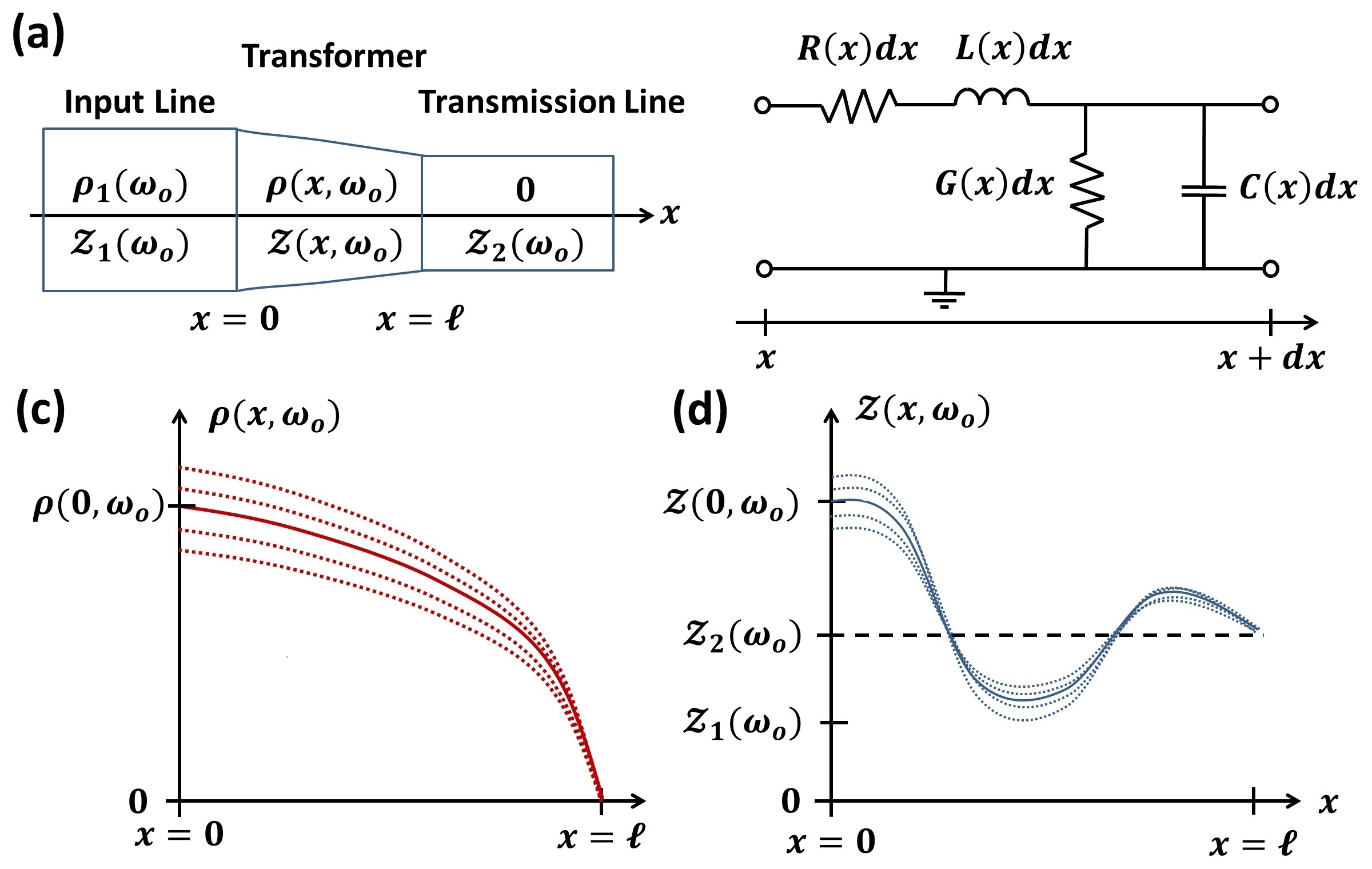
We consider an input line with forward-traveling wave of frequency incident upon a transmission line possessing a tapered interval , as in Fig. 1(a). The boundary between input and transmission lines is at . The characteristic impedance of the input line is , whereas in the tapered interval it is . As , smoothly transitions to of the transmission-line interior, i.e., . The measurable reflection coefficient of the traveling wave within the input line is while inside the taper it is .
In Appendix A we derive the Riccati differential equation of Walker and WaxWalker and Wax (1946) satisfied by ; importantly, we include the accompanying boundary conditions. Assuming , the equation may be expressed in linearized form as
| (1) |
with representing the propagation coefficient. From Eqs. (63) and (65), the accompanying boundary conditions at and are, respectively,
| (2a) | |||
| (2b) | |||
To determine the optimal tapered impedance transformer we minimize . Ultimately, we want to set , but important information can be obtained through a formal minimization. From Eq. (2a) we see that can be reduced if a proper choice of and is made. This is possible because, unlike boundary conditions and , the boundary values of and are not firmly established.
In Eq. (1), depends on both and , which may be expressed as
| (3a) | |||
| (3b) | |||
respectively, where is the series impedance per unit length and is the shunt admittance per unit length. As described in greater detail in Appendix A, , , , and are the unit-length resistance, inductance, conductance, and capacitance, respectively, of the tapered region, as introduced via the ladder-type transmission-line model depicted in Fig. 1(b).
Our goal of minimizing may be described as adjusting the underlying values of independent variables and at each point of the taper, subject to fixed boundary conditions of and , such that the values of and , and thus also , may be altered to give boundary values and that make as small as possible. Panels (c) and (d) of Fig. 1 depict this idea, where the various curves of and are generated as and are varied. The solid curves have corresponding boundary values for and that render minimal. The underlying and of these solid curves define the optimal impedance transformer for the incident traveling wave of frequency .
To optimize in the manner of variational calculus,Mathews and Walker (1970) we vary both underlying functions and , holding endpoint fixed but allowing endpoint to float. Specifically, we let and where and but and . Since the variation of is equivalent to varying , we vary such that from Eq. (2a) we have
| (4) |
To obtain in Eq. (4), we first integrate Eq. (1) so that may be expressed as a functional of , and their derivatives, viz.
| (5) |
where is implicitly a function of , and derivatives. Then, using Eq. (5) to obtain , and subsequently setting in Eq. (4), we arrive at two Euler-Lagrange equations that may be expressed as
| (6) |
| (7) |
with boundary conditions at given by
| (8) |
Normally, one would solve Eqs. (6) through (8) for and . However, since is unknown, a more fruitful approach is to solve for in terms of and . This gives
| (9) |
where is an arbitrary function of and and are independent of . If we apply this form to the boundary conditions of Eq. (8) we further see that and . Thus, the reflection coefficient within the optimal transformer is of the form .
The arbitrariness of allows us immediately to set , or equivalently, . In this way, our optimization always results in the absolute minimum, . Specifically, we set in Eq. (2a) and solve for , obtaining a second boundary condition on , viz.
| (10) |
in addition to . Then, rescaling by letting , where is now the arbitrary function of , and incorporating the additional boundary condition of Eq. (10), we now have
| (11) |
where imposition of and ensures the boundary conditions of are satisfied. Assuming a physically meaningful solution for and exists, Eq. (11) is the optimal form of for any impedance transformer that eliminates input-line reflections, specifically for frequency .
Given the optimal form of , we may determine the optimal taper design by substituting Eq. (11) into Eq. (1). This yields the constraint
| (12) |
This equation determines optimal and , or equivalently, via Eqs. (3), optimal and .333Equation (12) involves functions of complex numbers, so it actually represents two real-valued equations. For an optimal lossless transformer this is sufficient to determine the characteristic impedance and the propagation coefficient because the former is a real number while the later is an imaginary number. However, for the case of an optimal lossy taper, it may not be possible to specify the optimal characteristic impedance and/or propagation coefficient definitively, unless additional information about the nature of the lossiness, i.e., the transmission-line series resistance and shunt conductance, is also provided. Since is an arbitrary function of , subject to and , there are an infinite number of optimal transformer designs, where each design is characterized by and .444Here resembles a gauge transformation on scalar field where is invariant.
Several key points of our variational approach are:
-
1.
The boundary condition of Eq. (2a) illustrates the discontinuity of the voltage reflection coefficient across the interface.
-
2.
A variation of the input line reflection coefficient, , with endpoint not fixed, is developed from Eq. (2a), applicable to a specific frequency of incident forward-traveling wave.
-
3.
The variation of employs the variation of and at each point along the length of the taper, which necessitates the variation of , the voltage reflection coefficient within the taper, since it depends on both and .
-
4.
The optimization of implies an optimal form for , as given by Eq. (11), where is subject to the stated boundary conditions; any other proposed form for will not correspond to an optimal .
-
5.
The optimal form of and , or equivalently and , are obtained from Eq. (12).
In what follows we narrow our discussion to the case of a lossless optimal impedance transformer.
III The Optimal Lossless Impedance Transformer
For the remainder of our discussion we assume input line, transformer, and transmission line are lossless, such that
| (13a) | |||
| (13b) | |||
| (13c) | |||
where and are, respectively, the transformer inductance and capacitance per unit length at . Also, , and , are the constant values of the input line and interior of the transmission line, respectively, with and .
In Appendix B we apply Eqs. (13) to Eq. (12) to obtain the solution of the optimal lossless impedance transformer. An important result, which follows from Eq. (77) and Eq. (78), is that of an optimal lossless transformer may be written in the form
| (14) |
where is a frequency characteristic of the impedance transformer, and is a real-valued function of satisfying the boundary conditions
| (15) |
In this way, any design of optimal lossless impedance transformer is characterized by both and .
Also in our analysis of Appendix B, via Eq. (79), the propagation coefficient of the lossless transformer is found to be a constant value, i.e., . In the literatureKlopfenstein (1956) one typically approaches the problem of finding an optimal impedance transformer by assuming is independent of . Here, using our variational approach, the optimal propagation coefficient is indeed independent of , the same value as in the interior of the transmission line.
Since the dispersion frequency of the transformer is , where is a wavenumber, the group velocity is , which is constant for any , allowing us to write . Similarly, for an incident signal of frequency , the phase velocity is . Thus, we may interpret as the time it takes for a signal of frequency to traverse the length of the transformer and be reflected back to the input-line/taper interface. In this case the signal wavelength is since .
Via Eq. (81), of the optimal lossless transformer may be expressed in terms of as
| (16) |
where, via Eq. (80), is a root of
| (17) |
Since is independent of , the inductance per unit length and the capacitance per unit length can be obtained from and , respectively.
We summarize the key points of the optimal lossless transformer as follows:
- 1.
-
2.
Therefore a general result is that the design of the optimal lossless transformer is defined by the choice of and .
-
3.
The frequency is characteristic of the geometry and material composition of the optimal lossless taper, and is therefore more or less fixed, save for some ability to change the geometry, such as via the transformer length .
-
4.
An important result of our variational approach applied to the lossless transformer is that the optimal propagation coefficient of this case, , is a constant in , i.e., , as demonstrated in Appendix B.
- 5.
III.1 Reflection Response of the Optimal Lossless Impedance Transformer
As mentioned earlier, the optimal lossless impedance transformer of Eqs. (16) and (17) guarantees zero input-line reflections only for an incident signal corresponding to frequency . To determine reflection-response characteristics of the transformer at any other frequency we first solve Eq. (1) for frequency , instead of frequency , but with characteristic impedance given by Eq. (16). The result is the reflection coefficient of the transformer with respect to , which after some algebra may be expressed as
| (18) |
where
| (19) |
Equation (19) is just the lossless limit of the reflection coefficient of Eq. (11), with given by Eq. (14) and independent of .
For arbitrary the input-line reflection coefficient is still of the form of Eq. (2a), but now
| (20) |
where is Eq. (18) at . Also, setting in Eq. (19) yields , the same as Eq. (10). Thus, substituting the form of Eq. (18) into Eq. (20), and making use of Eq. (10) for , we may write . Assuming , this may be approximated as , or from Eq. (18), we have
| (21) |
This is the small-reflection response of a traveling wave of frequency incident upon an optimal impedance transformer of design defined by and .
Equation (21) may be used to analyze the passband characteristics of any optimal lossless impedance transformer with characteristic impedance of form given by Eqs (16) and (17). As examples, we next consider the two wide-band cases delineated by the transformer characteristic frequency .555Another case of interest is that of setting the design frequency to in Eq. (21). This eliminates large reflection response attributable to and results in a V-like passband centered about frequency . We consider the definition of this type of notch filter to be a subject for follow-on research. Several important points the reader should keep in mind as we investigate these cases are:
-
1.
The optimal lossless transformer of design choice and has reflection coefficient within the taper, , given by Eq. (19).
-
2.
We may use the reflection-response function, of Eq. (21), to determine choices for and that exhibit specific wide-bandwidth characteristics.
-
3.
By construction in Eq. (21), and this is the only point of the versus curve where is precisely zero.
III.2 The Wide-Band High-Pass Lossless Impedance Transformer
Recall from our introductory remarks that a wide-band high-pass impedance transformer can be constructed if the design frequency is detuned from the characteristic frequency such that . This statement is made more explicit by examination of the reflection response of Eq. (21). First, note that by construction; this is always the case, no matter the value of . If we let then we have
| (22) |
where, from Eq. (17), we note as . This all but eliminates from the expression of the reflection response, except for its appearance in the Fourier-like integral of the numerator, where it acts to delineate the region of high reflections, , from that of low reflections, . An estimate of the passband is to describe it as the range of frequencies such that . From Eq. (16), the corresponding characteristic impedance is
| (23) |
The form of Eqs. (22) and (23) indicates that of the lossless high-pass transformer may also be expressed as , where is a constant. From Eq. (15), we have an alternative expression of the boundary conditions of , viz.
| (24a) | |||
| (24b) | |||
As mentioned, the Fourier-transform-like integral in the numerator of Eq. (22) defines the high-pass frequency regime to be . The choice of determines the extent to which is negligible over this interval. A good choice for may be obtained by examining the asymptotic expansion of the integral for . After repeated integration by parts times this expansion may be expressed as
| (25) |
where refers to the n-th derivative with respect to of , and the integral on the right side of the equation is the expansion remainder. A good high-pass transformer is one with a that eliminates the second-order term in on the right side of Eq. (25); a better one also eliminates the third-order term, and so on.
In Appendix C we demonstrate how a -degree polynomial choice for can be used to eliminate terms of Eq. (25) to order in . Using this -degree polynomial as our , we obtain a reflection response and characteristic impedance expressable as
| (26) |
| (27) |
respectively, where is the gamma function, is a spherical Bessel function, and
| (28) |
is a regularized incomplete beta function.(Abramowitz and Stegun, 1972, p. 263) By construction we have as ; conversely, as , we find .
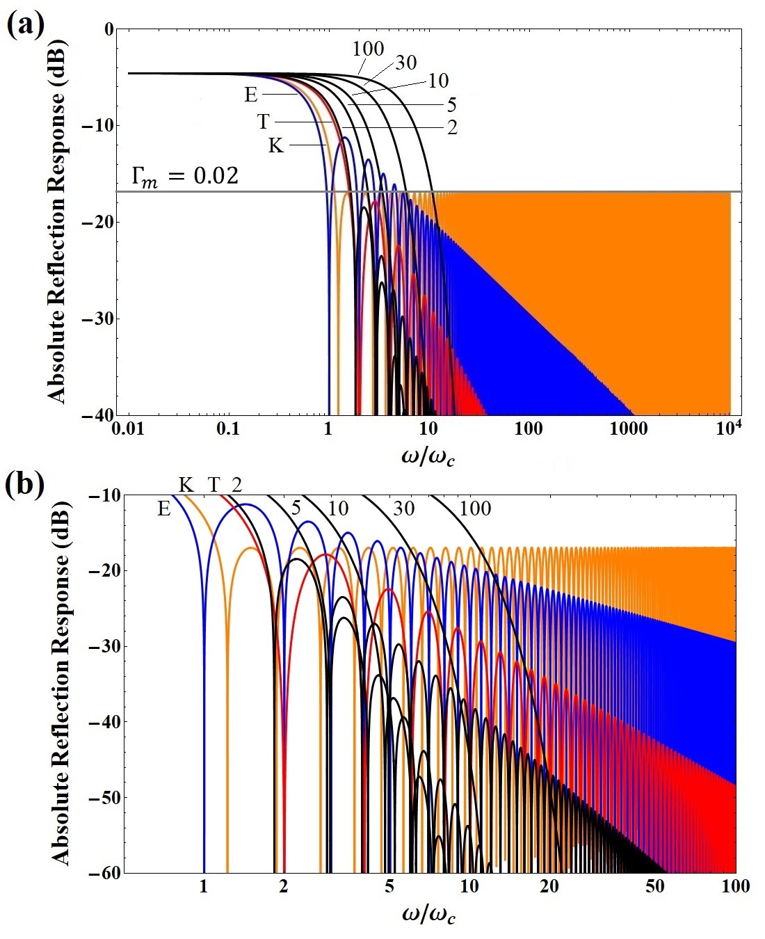
We illustrate our results with the specific example of a wide-band high-pass lossless transformer placed between a input line and load-bearing line. In this example our goal is a design with bandpass of - GHz, appropriate for a supconducting parametric amplifier, with high-frequency asymptotic reflections damped as strongly as possible. For concreteness, assume a transformer length of mm, with pH/m, pF/m, pH/m, and pF/m. In this case the characteristic frequency of the transformer is MHz, but this frequency can be adjusted by changing the value of .
In Fig. 2(a) we plot the absolute reflection response obtained from Eq. (26) as a function of the ratio of the input-signal frequency to the transformer characteristic frequency , on a logarithmic scale, for design values , , , , and . For comparison we also plot the absolute reflection response of the exponential, triangular, and Klopfenstein tapers that are described in Pozar.Pozar (2012) Our example is constructed to match the example in the Pozar text as closely as possible. In particular, for the Klopfenstein-taper parameters, corresponding to a ripple of 2%, we set , , and . For the Klopfenstein characteristic impedance we used the formula given by Pozar,Pozar (2012) viz.
| (29) |
where is a modified Bessel function of integer order. For the reflection response, we applied Eq (29) to Eq. (1) and solved for the reflection coefficient, then set to obtain the input-line reflection response. The result may be expressed as
| (30) |
where the last step follows from the Klopfenstein ansatz.Klopfenstein (1956) Note that the Klopfenstein model is not optimal because the characteristic impedance of Eq. (29) does not satisfy all of the boundary conditions of Eq. (24). Similarly, one can show that both the triangular and exponential models are not optimal because their respective characteristic impedances also do not satisfy Eq. (24).
In Fig. 2(b), we show the drop-off of absolute reflection response for a range of input frequencies starting from . This provides a comparison of the ripple response of the different taper designs. The -degree polynomial tapers have the smallest residual ripple, even for the case of , owing to the built-in behavior as . At , the maximum absolute reflection responses of the exponential and triangular tapers are approximately dB and dB, respectively, while the Klopfenstein ripple retains a fixed maximum of 2%, as per the parameter setting, i.e., dB. At the -degree polynomial cases of , , , , and are all well below dB.
For the superconducting parametric amplifiers discussed in the introduction, in the operating range of - GHz, the highly-damped reflections of the -degree polynomial design can substantially limit signal-gain ripple, as induced by impedance mismatch. A caveat of the -degree polynomial design is that as increases the lower bound of the passband tends to shift to higher frequencies, as is evident in Fig. 2(a). In particular, from Eq. (95) of Appendix C, we have
| (31) |
indicative of the passband diminishing to zero width as . This result is consistent with the Bode-Fano criterionBode (1955); *Fano1950-1 in the sense that as one might suspect the passband becoming a region of perfectly zero reflections since as ; however, the order in which one takes limits matters, so as for arbitrary the bandwidth instead goes to zero. For modest increases in , the tendency for the lower bound of the passband to shift to higher frequencies can be compensated for in the taper design by increasing the length of the taper, thereby decreasing .
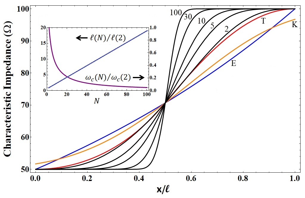
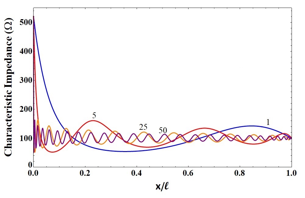
In Fig. 3, we plot the characteristic impedance, corresponding to the the absolute reflection response of Fig 2, as a function of relative position within the taper. The characteristic impedance of Eq. (27) is shown for design values of , , , , and , while that of the exponential, triangular, and Klopfenstein tapers is as in the Pozar text.Pozar (2012) Recall from Fig. 2(a) and the discussion of Eq. (31) that the lower bound of the passband shifts to higher frequencies as increases. To maintain a fixed lower bound we must allow to increase accordingly, i.e., becomes smaller. Specifically, to compare the characteristic impedance of a -degree polynomial taper () to that of the other taper designs in Fig. 3, we fix the lowest frequency of the -degree-polynomial passband, , such that for all . In this way, all of the -degree polynomial tapers will have the same bandwidth as the case, comparable to the bandwidths of the exponential, triangular, and Klopfenstein tapers. Since the lower bound of the Klopfenstein passband is typically defined as the frequency corresponding to the first zero of reflections, we may define similarly. Thus, from Eq. (26), the first zero of is the first zero of the spherical Bessel function , call it , i.e., such that
| (32) |
where . For example, first zeros of the spherical Bessel function include , , and . Then, setting implies
| (33) |
The inset of Fig. 3 is a plot of Eq. (33) as a function of increasing , showing both , corresponding to the left vertical axis, and , corresponding to the right vertical axis. For example, in order that the case have the same passband as the case, must be approximately times greater than . In particular, as then , corresponding to a taper of unattainably infinite length. Moreover, all of the curves corresponding to are difficult to realize physically given the length of transformer required, as well as the material composition and other geometric factors, i.e., , that contribute to .
In Fig. 3, note that the characteristic impedance of the case of the -polynomial taper design closely matches that of the triangular taper, but with a more strongly damped reflection oscillation, due to the behavior of the input-line reflections as . As increases the damping of these reflections increases as , and the shape of the characteristic impedance approaches a sharper profile for . The point is fixed for all .
In Fig. (3), the sharpness of the characteristic impedance profile as makes it difficult to fabricate such a taper due to limitations of line composition and geometry, as mentioned earlier. Even for the case of the taper, where from Fig. 2(a) the reflection response is negligible for , there is a sharp change in the characteristic impedance for that would make this taper extremely challenging to fabricate, given the necessary length of the taper. A compromise is to select a value of between the and cases. Clearly, a good choice is , but a better choice might be or . The best choice is to select the largest permitted by the fabrication constraints of the application such that residual oscillations are damped to the greatest extent possible within the region of exploitable passband—this is the physical limit of the high-pass design for the application.
Important points regarding the optimal wide-band high-pass transformer are:
-
1.
By setting the design frequency of the transformer to infinity we realized a high-pass bandwidth the order of .
-
2.
To exploit this bandwidth to its greatest extent we expanded the Fourier-like integral of the numerator of Eq. (22) in an asymptotic series, and we choose so as to eliminate the lowest terms of this series, as described in detail in Appendix C; this defined a model parametrized by integer , where the reflection response, by construction, is as .
- 3.
-
4.
We compared this optimal high-pass transformer model to the Klopfenstein, triangular, and exponential models, demonstrating its superior reflection response at high frequencies; this resulted from the optimal form of Eq. (22), which allowed us to design the asymptotic behavior.
-
5.
The Klopfenstein, triangular, and exponential models are not optimal transformers because their respective characteristic impedances do not satisfy the boundary conditions of Eq. (24).
-
6.
A limitation on the size of integer of the optimal design is imposed by the physical composition and geometry of the taper; a value in the range of of is probably reasonable for most applications.
III.3 The Wide-Band Low-Pass Impedance Transformer
In a manner analogous to the high-pass transformer, recall from our introductory remarks that a wide-band low-pass impedance transformer can be constructed if the design frequency is detuned from such that . In this case Eq. (21) becomes
| (34) |
where is determined from Eq. (17), for the case , viz.
| (35) |
As in Eq. (22) of the high-pass case, delineates the low-frequency and high-frequency regimes. From Eq. (16), the corresponding characteristic impedance is
| (36) |
As in the high-pass case, we can determine a choice for by considering the asymptotic behavior of the Fourier-transform-like integral of Eq. (34) as . Assuming , and repeatedly integrating by parts times, we obtain
| (37) |
where the last term is the expansion remainder, and we have defined
| (38) |
In Appendix D we demonstrate how a -degree polynomial choice for can be used to eliminate terms of Eq. (37) to order in . In this case the reflection response and characteristic impedance are
| (39) |
| (40) |
respectively, where is Kummer’s confluent hypergeometric function(Abramowitz and Stegun, 1972, p. 504) and is a Jacobi polynomial of order .(Abramowitz and Stegun, 1972, p. 561) By construction as ; conversely, as , we find .
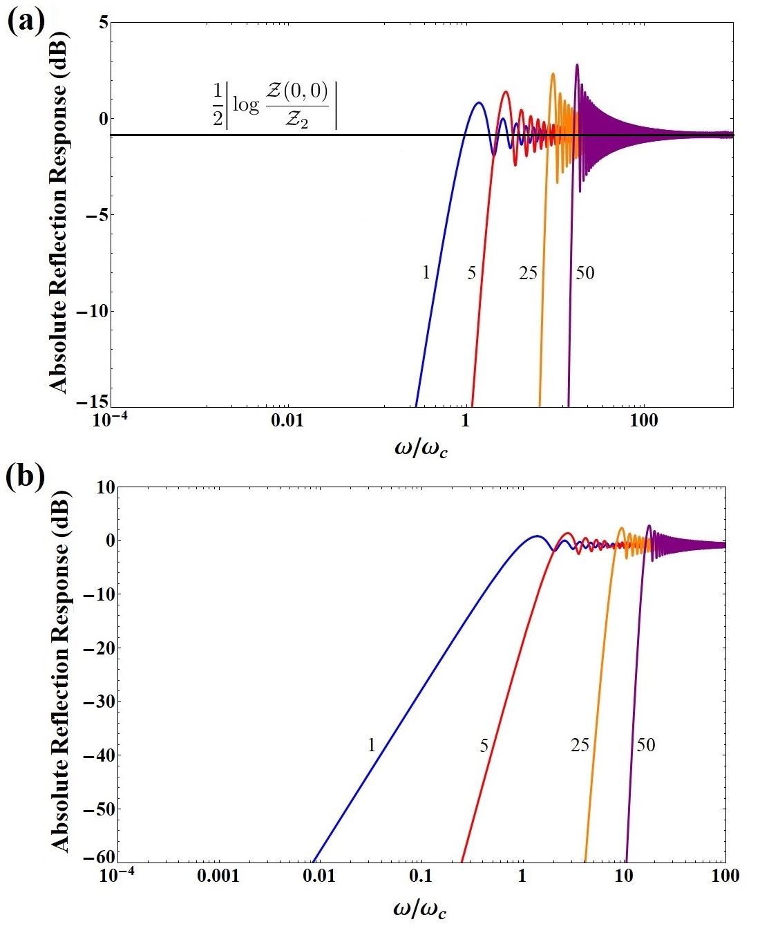
As in the high-pass case, we illustrate the wide-band low-pass lossless transformer with the specific example of a input line and load-bearing line. For concreteness, assume a transformer length of mm, with pH/m, pF/m, pH/m, and pF/m. Therefore, we have a bandpass that extends up to the transformer characteristic frequency, GHz. Again, this frequency can be adjusted by changing the length of the transformer.
In Fig. 4(a) we plot the absolute reflection response , as obtained from Eq. (39), as a function of the ratio of the input-signal frequency to the transformer characteristic frequency , on a logarithmic scale, for design values of , , , and . The figure shows negligible reflection response over a bandpass of up to , followed by a region characterized by large oscillating reflections. For the magnitude of reflections surpasses unity by as much as a factor of two due to the breakdown of the small-reflection approximation of Eqs. (1) and (21). This could be addressed by solving the full Riccati equation for the voltage reflection coefficient. However, the small-reflection approximation of Eq. (1) is more than adequate to estimate the breadth of the transformer pass band. In particular, we see from Fig. 4(b) the smallness of the bandpass reflections as the frequency decreases from .
In Fig. 5 we plot the characteristic impedance of the wide-bandwidth low-pass lossless transformer as a function of relative position within the taper, for values of , , , and . The figure illustrates the discontinuity in characteristic impedance at the interface that is particular to the low-pass transformer, independent of taper design choice. In this example the input line characteristic impedance is and just inside the taper we have . The discontinuity is governed by the size of the impedance mismatch between input and load-bearing lines, with solution for obtained from Eq. (35). As the impedance mismatch increases, fabrication of the transformer becomes a challenge because the taper characteristic impedance sharply increases at . This is the principal difficulty in building the low-pass impedance transformer, regardless of design choice.
Nevertheless, the solutions of the -degree polynomial design indicate the direction to take in fabricating the low-pass transformer, if the impedance mismatch is not too great. In Fig. 5, as increases the -degree polynomial solution incurs greater undulation, which again presents fabrication difficulties. From Eq. (116), the undulation behavior of may be approximated as
| (41) |
where . However, as Fig. 4 shows, the simplest case of has negligible reflection response over frequency band , with corresponding characteristic impedance of Fig. 5 exhibiting a very smooth and gradual undulation—only representing a challenge to fabrication at the end of the taper. Therefore, the case can represent a feasible design for an optimal low-pass transformer. Similar to the polynomial designs of the high-pass transformer, the largest value of that can be accommodated by fabrication constraints represents the best physical taper design.
An interesting aspect to the low-pass transformer is its ability to act as a filter of high frequencies. In Fig. 4(a), the black horizontal line is the asymptote for the limit of the absolute reflection response , as input frequency , independent of . When the asymptote approaches unity the low-pass transformer acts as low-pass filter, suppressing transmission of frequencies . In this limit we can approximate from Eq. (35) as , where . The absolute reflection response is then as . Thus, as the impedance mismatch between input line and load-bearing line increases, the filter becomes more effective. Efficacy of the device is limited by fabrication constraints imposed by the mismatch at the interface, as discussed earlier, but the device may have application to reduction of the Purcell effect (at GHz) in superconducting transmon and Xmon qubit-readout measurements.Reed et al. (2010); *Jeffrey2014; *BronnNT2015; *Sete2015
Important points regarding the optimal wide-band low-pass transformer are:
-
1.
By setting the design frequency of the transformer to zero we realized a low-pass bandwidth the order of .
-
2.
Analogous to the high-pass case, we exploited this bandwidth to its greatest extent by expanding the Fourier-like integral of the numerator of Eq. (34) in an asymptotic series, choosing so as to eliminate the lowest terms of this series, as described in detail in Appendix D; this again defined a model parametrized by integer , where the reflection response, by construction, is as .
- 3.
-
4.
We compared optimal low-pass transformer designs of different values of integer , plotting reflection response versus frequency in Fig. 4 and characteristic impedance versus position along the taper in Fig. 5; the small-reflection approximation employed in Fig. 4 tends to break down at high frequencies and larger values of .
IV Concluding Remarks
We presented a variational approach to determine the optimal form of the reflection coefficient of a tapered impedance transformer of length , for a specific design frequency . We used this result to construct the characteristic impedance and input-line reflection response of an optimal lossless transformer, defining the optimal transformer design in terms of and a real-valued function satisfying the boundary conditions of Eq. (15). The input-line reflection response was shown to depend on a characteristic frequency , where is the constant transformer group velocity.
By construction the input-line reflection response, as a function of arbitrary frequency , is zero specifically at , indicative of narrow pass band. However, we showed that if is detuned far from then, for an extended range of frequencies about , the magnitude of input-line reflections is negligible. Specifically, when we took the limit we obtained a high-pass transformer design with pass band , where the input-line reflection response and characteristic impedance are given by Eqs. (22) and (23), respectively. Similarly, when we took the limit we obtained a low-pass transformer design with pass band , where input-line reflection response and characteristic impedance are given by Eqs. (34) and (36), respectively.
Having derived a general form for wide-bandwidth transformers in terms of , for both the high-pass and low-pass frequency regimes, we then showed, for each regime, how to choose a polynomial that produces the widest exploitable pass band possible. In the case of the high-pass transformer, we compared our results to existing optimal taper designs, specifically the exponential, triangular, and Klopfenstein tapers described in Pozar.Pozar (2012) We showed that are our design exhibits superior pass-band characteristics. For the case of the low-pass transformer, we demonstrated the inherent difficulty of fabrication of the end of the taper, due to the discontinuity of the characteristic impedance at this interface. Nevertheless, we proposed the case of our design as the simplest to fabricate, with greater efficacy the smaller the impedance mismatch of the application.
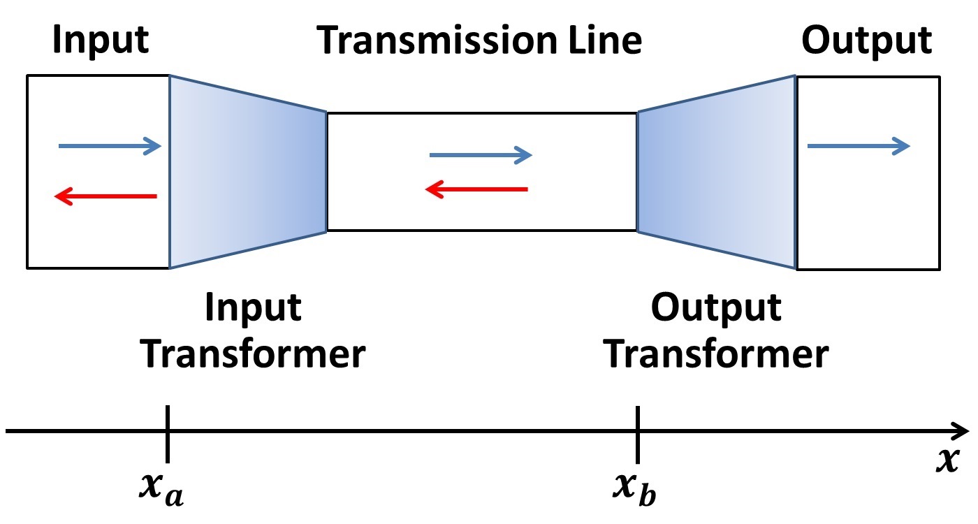
An important point to note is that our theory has focused on an isolated impedance transformer, one for which signals do not enter the transformer from the side. In practice, a transformer can be placed at both input and output of a load-bearing component, which means that the two transformers will be coupled, as in the example schematic of Fig. 6. Just as a forward-traveling wave (arrow pointing to right) can reflect from the input transformer, upon transmission through the input transformer, a forward-traveling wave can also reflect from the output transformer, allowing this reflected signal to encounter the input transformer from the right, as pictured.
In the case the two coupled transformers of Fig. 6, the optimization of their design requires simultaneous minimization of the voltage reflection coefficients at both and , from the left. This can be performed in the manner of our variational approach, but also requires derivation of the corresponding coupled Riccati differential equations of the two tapers, as well as their boundary conditions. These equations can be obtained by extending the approach used in Appendix A. We consider the case of coupled transformers to be an extension of our present work, and a subject of future focus.
As mentioned earlier, our motivation for the present study is to improve the signal-to-noise ratio of superconducting amplifiers used in quantum-information research. We are presently engaged in fabrication and validation of the transformer designs derived here, for the coplanar waveguides that comprise our amplifiers. One aim of our experimental analysis is to ascertain the limit of fabrication techniques to capture and leverage improvements implied by these designs, i.e., whether these transformers may be fabricated to sufficiently high precision to realize their performance benefits. The present theoretical results, and the findings of our follow-on experimental studies, may have broad applicability to the new and burgeoning fields of high-speed electronics, particularly where sensitivity to small reflections at an input-line/load-bearing interface is of critical importance.
Acknowledgements.
This work was supported by the Army Research Office and the Laboratory for Physical Sciences under EAO221146, EAO241777 and the NIST Quantum Initiative. RPE and Self-Energy, LLC acknowledge grant 70NANB17H033 from the US Department of Commerce, NIST. We have benefited from discussions with D. Pappas, X. Wu, M. Bal, H.-S. Ku, J. Long, R. Lake, L. Ranzani, K. C. Fong, T. Ohki, and B. Abdo.Appendix A Derivation of the Differential Equation of the Reflection Coefficient of an Impedance Transformer
Consider an input line and load-bearing transmission line with mismatched characteristic impedances and , respectively. A tapered impedance transformer of length is fabricated within the transmission line to address the mismatch, as in Fig. 1(a). Each of these three components is modeled as a ladder-type transmission line with unit-length series inductance , series resistance , shunt capacitance , and shunt conductance , comprising a ladder rung at extending over the infinitesimal length , as in Fig. 1(b). Within the input line (interior of the transmission line) , , , and are all constant and denoted by subscript 1 (2), whereas in the transformer these quantities vary with position , . Voltage and current at satisfy transmission-line equations given by
| (42a) | |||
| (42b) | |||
These equations also apply in the input line (interior of the transmission line), except that , , , and are replaced by , , , and (, , , and ).
A.1 Region Before the Taper
Within the region before the taper, i.e., in Fig. 1(a), for a traveling-wave of frequency , the solution of the input line is of the form
| (43a) | |||
| (43b) | |||
Substituting this into the input-line form of Eqs. (42) we obtain
| (44a) | |||
| (44b) | |||
where we have defined to be a line impedance per unit length and is a shunt admittance per unit length. If we assume amplitudes with spatial dependence of the form and then
| (45a) | |||
| (45b) | |||
such that a non-trivial solution of and requires , where . So we have two solutions we may express as a superposition, viz.
| (46a) | |||
| (46b) | |||
where the input-line characteristic impedance is . The amplitude () is that of a forward (backward) traveling wave. In keeping with convention, we may define the reflection coefficient of the input line as the ratio of backward-traveling voltage amplitude to forward-traveling voltage amplitude, viz. .
A.2 Region After the Taper
In the interior of the transmission line, after the taper, i.e., , the solution follows similarly to the region before the taper, viz.
| (47a) | |||
| (47b) | |||
However, in this case there is no backward-traveling component; one has instead
| (48a) | |||
| (48b) | |||
where , , and also , . In the limit then Eq. (43) matches to Eq. (47) at , resulting in
| (49a) | |||
| (49b) | |||
With , the above equations imply
| (50) |
which is in the absence of a transformer.
A.3 Region of the Taper
The region of the taper corresponds to . Since here the unit-length series impedance and shunt admittance vary with distance we segment the taper into subregions small enough that these quantities may be considered constant in each subregion. We then solve for voltage and current in each subregion, as we did for the regions outside the taper, with the caveat that we have to join solutions of the subregions together to obtain the full solution across the length of the taper. Once we accomplish this we can join this full solution of to that of and .
Specifically, we segment the taper into subregions where the n-th subregion corresponds to interval , of length , i.e., , with and . If is sufficiently narrow then constituents of impedance and admittance of the n-th subregion may be denoted by constant values , , , and , such that and . Then the equations governing the voltage and current of the n-th subregion are of the same form as those before the taper, i.e., , viz.
| (51a) | |||
| (51b) | |||
where we may write
| (52a) | |||
| (52b) | |||
where and .
At we may match the solution of to that of , viz.
| (53) | |||
| (54) |
As one passes to the continuum limit wherein
| (55) |
Applying these limiting results to the two boundary equations at , then as we find
| (56) |
| (57) |
Solving for the derivatives of the amplitudes in these two equations yields
| (58) |
| (59) |
These are the first-order differential equations governing the solution of the amplitudes of the taper region, .
As we did for the region before the taper, we may define a reflection coefficient for a position within the taper as , which has a derivative with respect to given by
| (60) |
If we substitute Eqs. (58) and (59) into Eq. (60) we obtain
| (61) |
This is the expression derived by Walker and Wax.Walker and Wax (1946) We next consider boundary conditions applicable to this differential equation.
First, at , we can equate the current and voltage of Eqs. (43), corresponding to the region before the taper, to the current and voltage of Eqs. (51), corresponding to the subregion of , just inside the taper. As the result is
| (62a) | |||
| (62b) | |||
where the reflection coefficient of the input line is and, similarly, the reflection coefficient of the taper at is . If we divide the first equation into the second and solve for we find
| (63) |
The reflection coefficient is discontinuous across the physical boundary at unless the two lines on either side of the interface have the same characteristic impedance at .
Similarly, at , we can consider the continuity of current and voltage across this interface using Eqs. (51), corresponding to the subregion of , just inside the taper, and Eqs. (47), corresponding to the region after the taper. As we find
| (64a) | |||
| (64b) | |||
Again, dividing the first equation into the second and solving for , we obtain
| (65) |
If the interface at is not a physical one then , which implies .
Appendix B Physically Meaningful Solutions of the Lossless Impedance Transformer
To obtain the solution of the lossless impedance transformer we apply Eqs. (13) to Eq. (12). Separating Eq. (12) into real and imaginary parts, we may write
| (66) |
| (67) |
where and . As in our earlier discussion of the more general case, for the lossless transformer a viable choice of , i.e., in Eq. (11), depends on the existence of a physically meaningful solution of and . As we shall show, restrictions on the solution will narrow the possible choices for .
For example, consider Eqs. (66) and (67) in the limit , viz.
| (68) |
| (69) |
We see in Eq. (69) that the real part of the integral of must vanish since alternatively (i) , corresponding to a trivial solution of impedance matching, or (ii) , which implies an infinite group velocity at the materials interface. Thus, inclusive of the boundary conditions of stated in Eq. (11), constraints imposed on are
| (70) |
As another example, since , we have from Eq. (67) that
| (71) |
where, via L’Hospital’s rule, we find
| (72) |
However, unless as , the above limit will be unbounded since via Eq. (11). Therefore, insisting be zero at , we may use L’Hospital’s rule again, viz.
| (73) |
Thus, additional constraints imposed on our choice of are
| (74) |
As a last point of observation, we note from Eq. (71) that
| (75) |
Since this limit requires
| (76) |
otherwise we would again have . Thus, Eqs. (70), (74), and (76) summarize the constraints on our choice of to ensure a physically meaningful solution of and , if one does indeed exist.
The task of choosing , subject to the constraints of Eqs. (70), (74), and (76), is made easier noting these constraints are satisfied if is written in the form
| (77) |
where the real-valued function , in turn, satisfies the boundary conditions
| (78) |
Thus, the definition of an optimal lossless impedance transformer reduces to choosing a real-valued that satisfies the boundary conditions of Eq. (78).
We may express the solution for the optimal lossless impedance transformer in terms of . To start, using of Eq. (77), the solution of in Eq. (71) becomes
| (79) |
since . Thus is constant in , along the entire length of the optimal impedance transformer, for any choice of .
Then, making use of Eqs. (77) and (79), we have from Eq. (68) the result
| (80) |
which determines the solution of . Similarly, solving for in Eq. (66), with the aid of Eqs. (77), (79), and (80), we arrive at
| (81) |
Thus, once we determine from Eq. (80) we may obtain via Eq. (81). The solutions for the inductance and capacitance per unit length then follow as
| (82) |
Appendix C Derivation of the Wide-Band High-Pass Lossless Impedance Transformer
A -degree polynomial
| (83) |
can be chosen for to eliminate all terms to order on the right side of Eq. (25). Here, polynomial coefficients , and scaling factor , are real-valued, and satisfies the boundary conditions of Eq. (15) via constraints
| (84) |
The second-order term on the right of Eq. (25) is removed in the limit when the equation is divided by
| (85) |
Higher terms are eliminated by requiring and for . The form of the polynomial guarantees while is obtained if
| (86) |
The coupled linear algebraic Eqs. (84) and (86) determine coefficients of the polynomial.
Substituting Eq. (83) into Eq. (22) for , and taking the limit , we may write
| (87) |
where we define and note polynomial coefficients now satisfy
| (88) |
Including the definition , the solution of Eq. (88) is
| (89) |
Similarly, substituting Eq. (83) into Eq. (23) for , and taking the limit , the corresponding characteristic impedance is
| (90) |
Equations (87), (89), and (90) define the high-pass transformer design of the -degree polynomial choice for .
Expanding in an infinite sum, an alternate expression of Eq. (87) is
| (91) |
The coefficients of Eq. (89) satisfy the summation identities
| (92a) | |||
| (92b) | |||
Using Eq. (92a) and (92b) to evaluate the sums over in Eq. (91), we have
| (93) |
where in the last step we recognize the resulting sum as Kummer’s confluent hypergeometric function, .(Abramowitz and Stegun, 1972, p. 504) Alternatively, , where is the gamma function and is a spherical Bessel function.(Abramowitz and Stegun, 1972, p. 509). Thus, we have
| (94) |
When we may use the asymptotic form of the Bessel function for large order,(Abramowitz and Stegun, 1972, p. 365) such that
| (95) |
Also, by construction, as .
With the aid of Eq. (92a), we may write Eq. (90) as
| (96) |
where we have introduced the sum
| (97) |
Differentiating with respect to and making use of Eq. (88), as well as the binomial theorem, we find derivative . Integrating from to we arrive at the expression
| (98) |
where
| (99) |
is a regularized incomplete beta function.(Abramowitz and Stegun, 1972, p. 263) Since then such that is a fixed point, the same for all , and Eq. (98) may be expressed alternatively as
| (100) |
With , as we havePagurova (1995)
| (101) |
Since if and if then
| (102) |
where is the Heaviside step function. Therefore, we may write
| (103) |
Appendix D Derivation of the Wide-Band Low-Pass Lossless Impedance Transformer
Analogous to the derivation of the wide-band high-pass lossless transformer, we construct a -degree polynomial
| (104) |
where satisfies the boundary conditions of Eq. (15) via constraints
| (105) |
To eliminate terms to order in of Eq. (37) we set for , which introduces additional constraints involving polynomial coefficients . Combining these constraints with those of Eq. (105) we obtain a set of coupled linear algebraic equations in that we may express as
| (106) |
The solution is
| (107) |
where we have included for completeness.
Substituting Eq. (104) into Eq. (34) for , we obtain
| (108) |
Expanding in an infinite sum, an alternate expression is
| (109) |
where we note that the sum over may be written in closed form as
| (110) |
Applying this last result to Eq. (109), and then shifting the sum over by , we obtain
| (111) |
Then, similar to the high-pass case, we recognize this sum to be related to Kummer’s confluent hypergeometric function, ,(Abramowitz and Stegun, 1972, p. 504) viz.
| (112) |
By construction, as we have . Conversely, as then ,(Abramowitz and Stegun, 1972, p. 508) so for fixed we have
| (113) |
The characteristic impedance corresponding to the design function is obtained by substituting Eq. (104) into Eq. (36) for . Within the resulting expression the derivative with respect to of is the Gauss series representation of the ordinary hypergeometric function .(Abramowitz and Stegun, 1972, p. 556) Alternatively, , where is a Jacobi polynomial of order .(Abramowitz and Stegun, 1972, p. 561) Hence, we have
| (114) |
where is given by Eq. (107). Therefore, the characteristic impedance may be written as
| (115) |
As we may use the Darboux formula for the large-order expansion of Jacobi polynomials.Szegő, G. (1975) Letting , this gives
| (116) |
where .
References
- Pozar (2012) D. M. Pozar, Microwave Engineering, 4th ed. (John Wiley & Sons, New York, 2012) pp. 261–267.
- Klopfenstein (1956) R. W. Klopfenstein, “A transmission line taper of improved design,” Proc. of the IRE , 31 (1956).
- Note (1) Specifically, in the Klopfenstein model of Ref (\rev@citealpnumKlopfenstein1956), as it is discussed in Ref. (\rev@citealpnumPozar2012), by a maximum reflection of 2% in the passband we mean the maximum reflection parameter is set to .
- Castellanos-Beltran et al. (2008) M. A. Castellanos-Beltran, K. D. Irwin, G. C. Hilton, L. R. Vale, and K. W. Lehnert, “Amplification and squeezing of quantum noise with a tunable josephson metamaterial,” Nature Physics 4, 928–931 (2008).
- Bergreal et al. (2010) N. Bergreal, F. . Schackert, M. Metcalfe, R. Vijay, V. E. Manucharyan, L. Frunzio, D. E. Prober, R. J. Schoelkopf, S. M. Girvin, and M. H. Devoret, “Phase-preserving amplification near the quantum limit with a josephson ring modulator,” Nature 465, 64–68 (2010).
- Spietz et al. (2010) L. Spietz, K. Irwin, M. Lee, and J. Aumentado, “Noise performance of lumped element direct current superconducting quantum interference de- vice amplifiers in the 4-8 ghz range,” Appl. Phys, Lett. 97, 142502 (2010).
- Hatridge et al. (2011) M. Hatridge, R. Vijay, D. H. Slichter, J. Clarke, and I. Siddiqi, “Dispersive magnetometry with a quantum limited squid parametric amplifier,” Phys. Rev. B 83, 134501 (2011).
- Hover et al. (2012) D. Hover, Y. F. Chen, G. J. Ribelli, S. Zhu, S. Sendelbach, and R. McDermott, “Superconducting low-inductance undulatory galvanometer microwave amplifier,” Appl. Phys. Lett. 100, 063503 (2012).
- Eom et al. (2012) B. H. Eom, P. K. Day, H. G. LeDuc, and J. Zmuidzinas, “A wideband, low-noise superconducting amplifier with high dynamic range,” Nature Physics 8, 623–627 (2012).
- Roch et al. (2012) N. Roch, E. Flurin, F. Nguyen, P. Morfin, P. Campagne-Ibarcq, M. H. Devoret, and B. Huard, “Widely tunable, nondegenerate three-wave mixing microwave device operating near the quantum limit,” Phys. Phys, Lett. 108, 147701 (2012).
- Mutus et al. (2013) J. Y. Mutus, T. C. White, E. Jeffrey, D. Sank, R. Barends, J. Bochmann, Y. Chen, Z. Chen, B. Chiaro, A. Dunsworth, J. Kelly, A. Megrant, C. Neill, P. J. J. O’Malley, P. Roushan, A. Vainsencher, J. Wenner, I. Siddiqi, R. Vijay, A. N. Cleland, and J. M. Martinis, “Design and characterization of a lumped element single-ended superconducting microwave parametric amplifier with on-chip flux bias line,” Appl. Phys, Lett. 103, 122602 (2013).
- Macklin et al. (2015) C. Macklin, K. O’Brien, D. Hover, M. E. Schwartz, V. Bolkhovsky, X. Zhang, W. D. Oliver, and I. Siddiqi, “A near-quantum-limited josephson traveling-wave parametric amplifier,” Science 350, 307–310 (2015).
- Vissers et al. (2016) M. R. Vissers, R. P. Erickson, H.-S. Ku, L. Vale, W. Xian, G. C. Hilton, and D. P. Pappas, “Low noise kinetic inductance ampliers using three wave mixing,” Appl. Phys. Lett. 108, 012601 (2016).
- Erickson and Pappas (2017) R. P. Erickson and D. P. Pappas, “Theory of multiwave mixing within the superconducting kinetic-inductance traveling-wave amplifier,” Phys. Rev. B 95, 104506 (2017).
- Mohebbi (2010) H. R. Mohebbi, Parametric Interaction in Josephson Junction Circuits and Transmission Lines, Ph.D. thesis, University of Waterloo (2010).
- Chaudhuri, Gao, and Irwin (2015) S. Chaudhuri, J. Gao, and K. Irwin, “Simulation and analysis of superconducting traveling-wave parametric amplifiers,” IEEE Trans. on Appl. Superconductivity 25, 1500705 (2015).
- Note (2) D. P. Pappas, private communication.
- Collin (1956) R. E. Collin, “The optimum tapered transmission line matching section,” Proc. of the IRE , 539 (1956).
- Bode (1955) H. W. Bode, Network Analysis and Feedback Amplifier Design, 10th ed. (Van Nostrand, New York, 1955) pp. 276–302.
- Fano (1950) R. M. Fano, “Theoretical limitations on the broad-band matching of arbitrary impedances,” J. of the Franklin Institute 249, 57–83 (1950).
- Walker and Wax (1946) L. R. Walker and N. Wax, “Non-uniform transmission lines and reflection coeffiicients,” J. of Appl. Phys. 17, 1043 (1946).
- Mathews and Walker (1970) J. Mathews and R. L. Walker, Mathematical Methods of Physics, 2nd ed. (Addison-Wesley, Reading, MA, 1970) pp. 322–340.
- Note (3) Equation (12) involves functions of complex numbers, so it actually represents two real-valued equations. For an optimal lossless transformer this is sufficient to determine the characteristic impedance and the propagation coefficient because the former is a real number while the later is an imaginary number. However, for the case of an optimal lossy taper, it may not be possible to specify the optimal characteristic impedance and/or propagation coefficient definitively, unless additional information about the nature of the lossiness, i.e., the transmission-line series resistance and shunt conductance, is also provided.
- Note (4) Here resembles a gauge transformation on scalar field where is invariant.
- Note (5) Another case of interest is that of setting the design frequency to in Eq. (21). This eliminates large reflection response attributable to and results in a V-like passband centered about frequency . We consider the definition of this type of notch filter to be a subject for follow-on research.
- Abramowitz and Stegun (1972) M. Abramowitz and I. A. Stegun, Handbook of Mathematical Functions: with Formulas, Graphs, and Mathematical Tables, 0009th ed. (Dover Publications, New York, 1972).
- Reed et al. (2010) M. D. Reed, B. R. Johnson, A. A. Houck, L. DiCarlo, J. M. Chow, D. I. Schuster, L. Frunzio, and R. J. Schoelkopf, “Fast reset and suppressing spontaneous emission of a superconducting qubit,” Appl. Phys. Lett. 96, 203110 (2010).
- Jeffrey et al. (2014) E. Jeffrey, D. Sank, J. Y. Mutus, T. C. White, J. Kelly, R. Barends, Y. Chen, Z. Chen, B. Chiaro, A. Dunsworth, A. Megrant, P. J. J. O’Malley, C. Neill, P. Roushan, A. Vainsencher, J. Wenner, A. N. Cleland, and J. M. Martinis, “Fast accurate state measurement with superconducting qubits,” Phys. Rev. Lett. 112, 190504 (2014).
- Bronn et al. (2015) N. T. Bronn, Y. Liu, J. Hertzberg, A. Corcoles, A. Houck, J. M. Gambetta, and C. J. M., “Broadband filters for abatement of spontaneous emission in circuit quantum electrodynamics,” Appl. Phys. Lett. 107, 172601 (2015).
- Sete, Martinis, and Korotkov (2015) E. A. Sete, J. M. Martinis, and A. N. Korotkov, “Quantum theory of a bandpass purcell filter for qubit readout,” Phys. Rev. A 92, 012325 (2015).
- Pagurova (1995) V. I. Pagurova, Encyclopedia of Mathematics: Incomplete Beta Function, Vol. 3 (Springer, Dordrecht, 1995) pp. 153–154.
- Szegő, G. (1975) Szegő, G., Orthogonal Polynomials, 4th ed., Vol. XXIII (American Mathematical Society Colloquium Publications, Providence, RI, 1975) p. 196.