Theoretical analysis of electrostatic energy harvester configured as Bennet’s doubler based on Q-V cycles
Key words and phrases:
Keywords: Q-V cycle, Bennet’s doubler, saturation voltage, electrostatic energy harvester.Key words and phrases:
Abstract – This paper presents theoretical analysis of a MEMS electrostatic energy harvester configured as the Bennet’s doubler. Steady-state operation of the doubler circuit can be approximated by a right-angled trapezoid Q-V cycle. A similarity between voltage doubler and resistive-based charge-pump circuit is highlighted. By taking electromechanical coupling into account, the analytical solution of the saturation voltage is the first time derived, providing a greater comprehension of the system performance and multi-parameter effects. The theoretical approach is verified by results of circuit simulation for two cases of mathematically idealized diode and of Schottky diode. Development of the doubler/multiplier circuits that can further increase the saturation voltage is investigated.1. Introduction
Wireless sensor nodes (WSNs) are emerging as one of the most commonly used monitoring and sensing systems [1, 2]. Currently, most WSNs are powered by batteries. Energy harvesting from vibration becomes a potential alternative to obtain electrical energy for WSNs, especially in some circumstances where batteries may not be feasible. For the vibration energy harvesters, there are three common transduction mechanisms which includes piezoelectric, electromagnetic and electrostatic [3, 4, 5]. In this paper, we focus on the electrostatic energy harvesting system.
One of the problems associated with the electrostatic energy harvesters is the implementation of power management circuits. As an example, a conversion circuit consisted of a voltage source, a variable capacitor and two switches was presented in [6, 7]. Although energy transduction through this circuit is possible, the regime where the output voltage saturated was not discussed. Several solutions based on energy-renewal technique for extracting electrical energy were presented. For instance, Yen et al. proposed a configuration of single variable-capacitance harvester, combining an asynchronous charge-pump with an inductive fly-back circuit to recharge the scavenging capacitor [8]. Mitcheson et al. developed a buck-boost topology with bi-directional switches for rectifying and increasing the AC voltage obtained from a transducer [9]. These circuit topologies face the trade-off between power consumption of control unit and harvester efficiency.
The Bennet’s doubler was early introduced in 1787 by the Reverend Bennet and Kaye [10]. The device is used for the continuous doubling of an initial small charge through a sequence of operations with three plates. Based on this approach, de Queiroz proposed a promising variation of such a voltage doubler for macro-scale vibration energy harvesters composed by variable capacitors and diodes [11, 12, 13]. In order to adapt the concept to micro-scale electrostatic generators, several researches have been developed and investigated [14, 15, 16, 17], including attempts to increase the charging current for a reservoir capacitor or to optimize the harvested power. In a recent work by Galayko [18], operation of the doubler configuration with a single variable capacitor was thoroughly analyzed in the electrical domain. The shape of Q-V diagram obtained from simulation is very close to be rectangular. However, operation of a transducer configuration with two time-varying capacitors and the dependence of the saturated voltage on dynamic characteristics of the mechanical domain has not explored yet.
Since the saturation phenomenon was observed in experiments [16], the effect of the electromechanical coupling on it is of interest to study. This paper further presents a theoretical analysis of the Bennet’s doubler based on the Q-V cycle. A complete model of an anti-phase overlap-varying transducers electrically configured as a voltage doubler is investigated. Numerical results for both ideal- and non-ideal diodes are obtained by means of a SPICE simulator, which are used to support the analytical solutions. For further increase of the saturated voltage across the storage capacitor, alternative topologies are introduced and analyzed.
2. Steady state operation with mathematically idealized diodes
2.1. Theoretical analysis
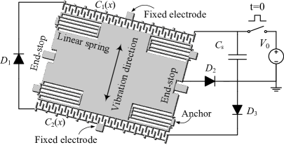
The overlap-varying energy harvesters can be utilized in a charge-doubling circuit-configuration as shown in Figure 1. The proof mass is suspended by four folded-beam linear springs. The maximum displacement is defined by the mechanical end-stops. Two anti-phase variable capacitors are connected to three diodes and the storage capacitor . Here and are the nominal capacitance, the nominal overlap and the proof mass displacement respectively. Operation of the doubler circuit does not require any control unit or switches but an initial bias voltage .
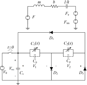
Figure 2 shows a complete lumped-model of the doubler configuration including equivalent circuit for the mechanical subsystem, where - proof mass, - mechanical damping, - total spring stiffness, - an external force, - the electrostatic force and - the parasitic capacitance of each transducer. The contact force is simply modeled as a spring-damper system for [19], where is relative displacement between the proof mass and the end-stops, is the impact stiffness and is the impact damping.
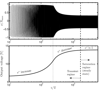
For a sufficient voltage and an adequate input acceleration amplitude , the voltage accumulated on the storage capacitor initially increases. The vibration frequency is chosen . Figure 3 shows that after certain cycles of transient regime, the steady state is achieved. The electrical energy is no longer harvested and the output voltage is then maintained constant at (i.e., saturation voltage).
| Parameters | Value |
|---|---|
| Proof mass, | 1.022 mg |
| Spring stiffness, | 3.595 N/m |
| Thin-film air damping, | 3.478e-5 Ns/m |
| Nominal overlap, | 80 m |
| Nominal capacitance, | 15 pF |
| Parasitic capacitance, | 7.5 pF |
| Storage capacitance, | 10 nF |
| Contact stiffness, | 3.361 MN/m |
| Impact damping, | 0.435 Ns/m |
| Maximum displacement, | 80 m |
The proof mass displacement amplitude changes in complicated manner: first reaches the maximum value (i.e., which is limited by the mechanical end-stops), then decreases and kept fixed at in saturation regime. For convenience, we define the rate of voltage evolution as a ratio of the maximum output voltage in two subsequent period
| (2.1) |
As shown in Figure 3, is modified over cycles under the variation of as follows. is small at the beginning and gradually increases, meanwhile . After reaching the maximum, decreases with reduction of and finally becomes one at steady state. Ultimately higher voltages through the conversion phase induce more effective electrical damping represented by electrostatic force in the transducers, causing a decrease of the proof mass displacement. As a consequence, the transducer capacitance ratio is reduced to , which is no more satisfied the condition of the doubler circuit operation . Therefore, is saturated at a certain value. Detail of dynamic analyses and the model parameters (i.e., listed in Table 1) are referred to [20]. In this paper, the effect of the electrostatic force on is the major objective of investigation.
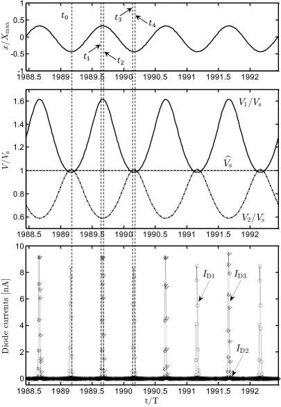

Figure 4 shows waveforms of the proof mass displacement, the voltages across and the currents through three mathematically idealized diodes respectively. Operation of the doubler circuit at steady state can be divided into a sequence of four stages from to . Based on the dynamic simulations, we observe that the relation of and at steady state can be approximated by a right-angled trapezoid Q-V cycle diagram and the time interval between and are very small, as depicted in Figure 5.
Stage I:
At , and , where is the maximum displacement at steady state. From to , all three diodes and are blocking as the condition is satisfied. The charges on the two transducers are
| (2.2) | ||||
| (2.3) |
In the first stage, and are constants, and are given
| (2.4) | ||||
| (2.5) |
Stage II:
At , and diode starts to conduct. Since the time interval between and is very small (i.e., see Figure 5), the proof mass displacement at can be approximated as , then
| (2.6) |
The solution is given as
| (2.7) |
The peak values of voltages across and are
| (2.8) | ||||
| (2.9) |
In this stage, charges and are pumped from into and respectively. At steady state, is considered unchanged, thus is neglected.
Stage III:
From to , all diodes are blocked, and are constants
| (2.10) | ||||
| (2.11) |
At , , and starts to conduct transferring amount of charge from into . Similarly, since is treated as constant, is thus negligible. The relation (2.1) now can be written as
| (2.13) |
Due to the small interval time between and , , resulting in . In other words, the charge transfered from into is insignificant.
Considering the voltage across the capacitor at
| (2.14) | ||||
Therefore, also starts to conduct at since the condition holds.
Stage IV:
From to , is conducting and is transfered from into . The charge is
| (2.15) |
The condition is fulfilled, showing that the state of the doubler circuit at is exactly the same as when , and a new cycle starts. This also proves that the right-angled trapezoid Q-V cycle diagram is capable of describing the operation of the doubler circuit.
2.2. Similarity of Bennet’doubler and charge-pump circuit
Among different circuit topologies for the interface electronics of MEMS capacitive energy harvesters [21, 22], the charge pump circuit early presented by Roundy et al. [23] is one of the most promising topologies. Another variation with inductive fly-back circuitry was developed by Yen et al. [8]. The simplest way to implement fly-back is to use a load resistance, originally reported in [24]. Such a fly-back configuration was thoroughly analyzed in [25].
Comparing the results shown in the literature with the one obtained in this paper, it is worth to note that the Q-V cycle for the charge pump circuit with resistive fly-back is very similar to that of Bennet’s doubler circuit. Both topologies can be approximated by trapezoidal conversion cycle. At the steady state of the idealized charge pump and the voltage doubler, the Q-V cycle is degenerated to a line (i.e., see Figure 5).
3. Approximation of the saturation voltage with mathematically ideal diode
The electrostatic force plays an important role in saturation of the output voltage and is thoroughly analyzed in this Section. is modeled as
| (3.1) |
where is the electrostatic energy of the transducers. and can be simplified as anti-phase sinusoidal signals for the sake of analysis although it is more complicated than that in reality. Based on the dynamic simulations, we observe that the phase difference between the input acceleration and the voltage across is negligibly small and is ignored. The waveforms of and are then presented as
| (3.2) | ||||
| (3.3) |
yielding
| (3.4) |
The coefficient is negligible, the electrostatic force is then
| (3.5) |
where . The harmonic term of is in phase with the input acceleration.
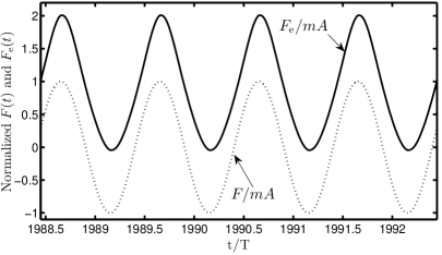
Figure 6 shows the comparison between the input acceleration and the electrostatic force, at the same time duration as Figure 4. These simulation results along with expression of in (3.5) confirm that our assumption is reasonable.
The differential equation of the spring-mass-damping system, which is set in continuous oscillation by a sinusoidal force acting on the mass, is
| (3.6) |
The steady-state solution of (3.6) is , where is the offset displacement and the harmonic term is [26]
| (3.7) |
where . Since and the proof mass displacement barely reaches its constraint, the peak value of is . The ratio obtained from simulations is less than for all g, therefore is assumed negligible. By considering amplitudes of the harmonic term and ignoring phase differences, the saturation voltage is
| (3.8) |
Although performance of the harvesting system using mathematically ideal diode is analyzed, the power loss due to diode imperfections such as leakage current and junction capacitance is still an open room for investigation. This issue will be explored in the next section.
4. Operation of the Bennet’s Doubler with Schottky diode
4.1. Approximated Q-V Cycle at steady state
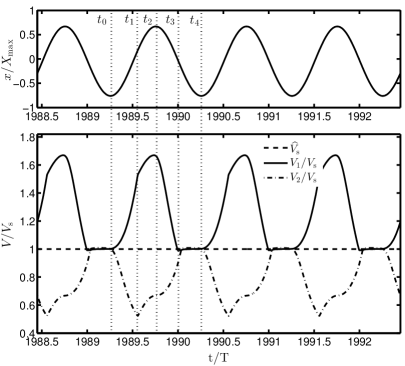
In the same manner of the Dragunov’s work [14, 27], the Schottky diode 1N6263 is used to assess effect of diode losses on the harvesting system performance, where the magnitude of reverse current is comparable with the charging current through the storage capacitor, and the zero bias junction capacitance is in the range of transducer nominal capacitance.


Figure 7 shows waveforms of the proof mass displacement and the voltages and across and respectively. Similarly, operation of the doubler circuit at steady state can be divided into a sequence of four stages, which is more clearly than considerations of mathematically idealized diode (i.e., the time interval between stages is significant). In general, the relation of and at steady state can be approximated by a right-angled trapezoid Q-V cycle diagram in Figure 8. Charges transferred from or into are neglected since the output voltage is unchanged at steady state. Differently from previous section, the proof mass displacements at and are still unknown.
Stage I:
The same as previous analysis, the charges on the two generators and variations of and from to are presented by equations (2.2), (2.3), (2.4) and (2.5).
Stage II:
At , , and diode starts to conduct, this yields
| (4.1) |
From to , charge is pumped from into .
Stage III:
From to , all diodes are blocked, and are constants that are described by (2.10) and (2.11). At , starts to conduct due to . This condition is expressed by (2.13), which results in
| (4.3) |
The voltage across at is
| (4.4) | ||||
As the condition is fulfilled, also starts to conduct at . Substituting (4.3) to (2.10), we get
| (4.5) |
Stage IV:
From to , is conducting and is transfered into from . At , and the state of the doubler circuit is the same as when , leading to
| (4.6) |
where
| (4.7) |
From the equations (2.2), (4.6) and (4.7), the displacement at is given by . As the consequence
| (4.8) |
Substituting this result back into (2.10) and (2.11), the voltages across and at are obtained
| (4.9) | ||||
| (4.10) |
At , starts to stop conducting since is slightly less than . This relation can be approximated as . Similarly as equation (4.1), we get
| (4.11) |
The solution of the maximum displacement at steady state is
| (4.12) |
Substituting (4.12) back into (4.1), the proof mass displacement at is determined by
| (4.13) |
Therefore, the peak values of and are
| (4.14) | ||||
| (4.15) |
and are then approximated by
| (4.16) | ||||
| (4.17) |
yielding
| (4.18) |
where
| (4.19) |
Since is negligible and , the electrostatic force can be given by
| (4.20) |
which is represented as
| (4.21) |
where .
Using the same analysis procedure in the previous section, the saturation voltage is
| (4.22) | ||||

Based on those analysis above, the completed Q-V diagram combined by both transducers is summarized in Figure 9.
4.2. Numerical validations
| Diode | [nA] | [pF] | [V] |
|---|---|---|---|
| 1N6263 | 3.87 | 1.77 | 0.39 |
| BAS716 | 3.52e-6 | 1.82 | 0.65 |
| BAT41 | 10.00 | 5.76 | 0.37 |
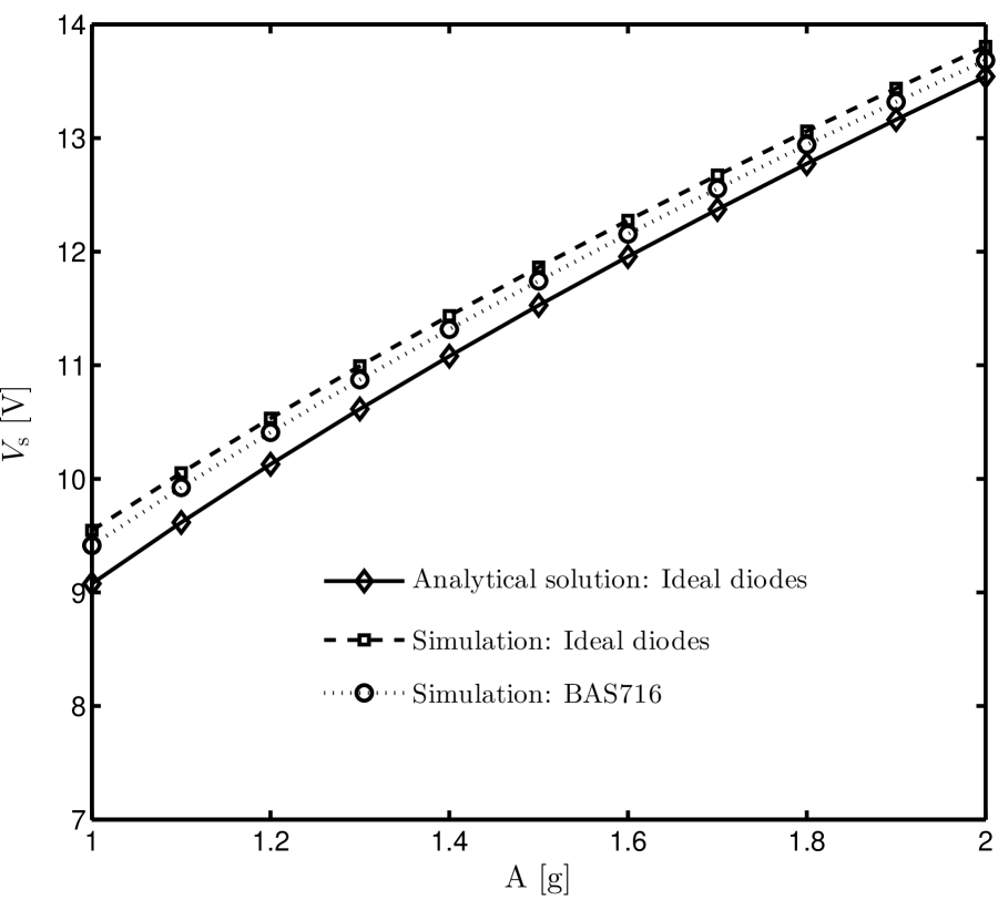
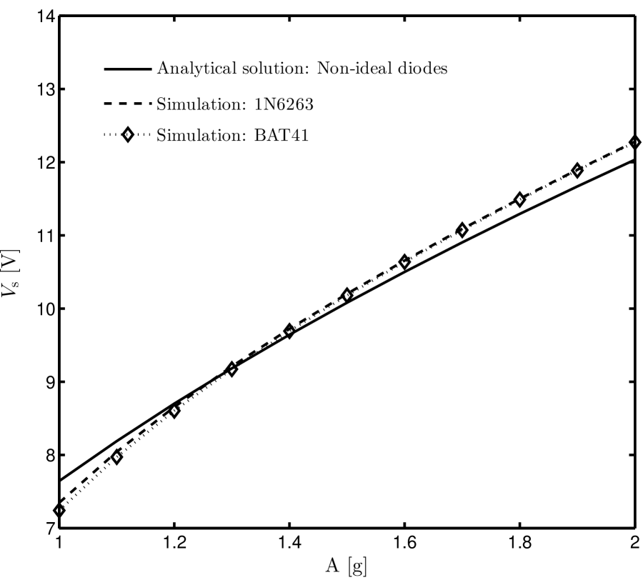
Figure 10(a) shows the saturation voltages for different acceleration amplitudes, where the simulation results with use of the mathematically idealized diode and the analytical solution expressed by formula (3.8) are compared. The figure also exhibits that the low-losses diode BAS716 performs very close to that of mathematically idealized diode. In the same manner, Figure 10(b) presents the comparison of the analytical solution obtained from (4.22) against the numerical simulations using different Schottky diodes. Despite of disparities in reverse current, junction capacitance and built-in junction voltage, both diodes 1N6263 and BAT41 give almost the same saturation voltages. The agreement between theoretical and numerical results in both cases verifies the predictions of our analytical approach and solutions. Diode parameters used on the simulations are listed in Table 2.
4.3. Effect of diode operation on mechanical dynamics
The Q-V cycle is a useful geometrical tool that enables us to realize the operation of voltage doubler circuit at steady state. However, the harvesting system performance in reality is more sophisticated, especially in transient time.
Based on dynamic simulations, we observe that the phases of the external force , the proof mass displacement and the electrostatic force are initially different. However, those differences gradually decrease due to effect of the diode states (i.e. blocked and conducting). This variation process leads to the negligible phase shift at steady state. Such a clarification supports the assumption that we made in theoretical analysis sections. In other words, the dynamic motion of the proof mass also strongly depends on both of the transducing force and the diode operation mechanism. This statement is valid when different diode models such as the mathematically idealized diode and the Schottky diodes are utilized.
5. Circuit topologies to improve the saturation voltage
5.1. A new voltage doubler with single switch
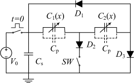
Although the diode plays an vital role for initially charging , in principle, it could be removed after a few transient vibration cycles. This also enlarges the charging current through the storage capacitor due to the relation . Therefore, it is worthwhile to investigate performance of the harvester when is disconnected. An electronic switch in series with can be used for this function, as shown in Figure 11.
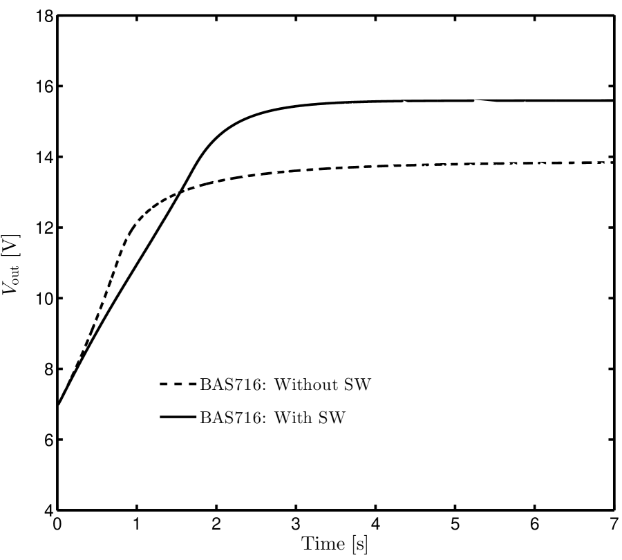
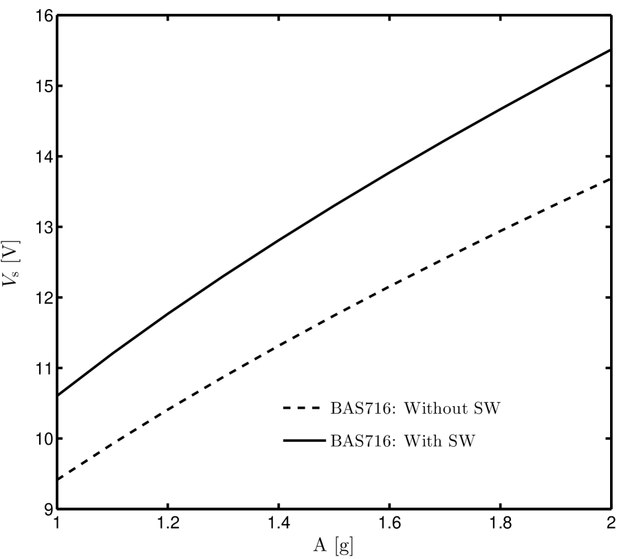
In the simulation, is only ON in the first several vibration cycles, then turned OFF to eliminate effect of on . Figure 12(a) shows evolution of the output voltage in two cases without and with presence of . Saturation voltage in the latter case is about V. This is a significant improvement over the 13.84 V achieved for the circuit topology in Figure 2. Similar results are obtained with different acceleration amplitudes in Figure 12(b).
5.2. Cockcroft-Walton generator applied to MEMS device

A common topology of voltage doubler further developed from the Greinacher circuit [28] is depicted in Figure 13, in which the feed-back diode is added to connect the storage capacitor and the two transducers. Both theoretical operation analysis and simulation results show that performances of the Bennet’s doubler and the Greinacher configuration are completely identical. The roles of three diode and are the same as they do in Figure 2.


Based on the Greinacher doubler circuit, a well-known voltage cascade was early proposed by the British and Irish physicists John D. Cockcroft and Ernest T. S. Walton in 1932 [29, 30]. The Cockcroft-Walton generator (i.e., named after the two authors) was proved to be able to generate a high DC voltage from a low-voltage AC, which therefore is interesting to be utilized for the micro-scale harvesters. Figure 14 shows the circuit diagram of the two-stage Cockcroft-Walton, in which the voltage across two capacitor and is the output voltage, called . The simplified operation of such a multi-stage voltage doubler is depicted in Figure 15. Similar to the Bennet’s configuration, operation of the Cockcroft-Walton multiplier can also divided into a sequence of four stages. At first, all diodes are blocked. In the second stage, and are simultaneously conducting and charges are transferred to and . All diodes are reverse-biased in the third stage. In the final stage, and are conducting, transferring the scavenged energy to and . is mainly used for pre-charging and its conduction during operation is insignificant and negligible.
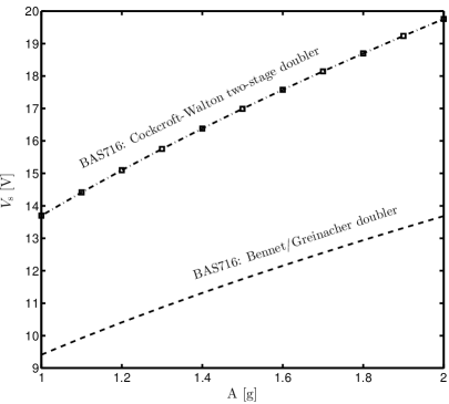
Figure 16 shows a remarkable increase of the saturation voltage when the Cockcroft-Walton multiplier and the Bennet’s doubler are compared. Since the topology discussed in Section 5.1 requires a control unit for controlling the switch, the Cockcroft-Walton multiplier is much more convenient to keep the simplicity in practical implementation. Furthermore, our simulations reveal that this circuit topology is capable of operating with very low ratio of capacitance variation . In particular, its minimum value is found , making such a circuit attractive for further investigation in future work.
6. Conclusion
This study presented a theoretical analysis of MEMS electrostatic energy harvesters configured as Bennet’s doubler at saturation regime, based on combination of Q-V diagram and dynamic simulations. The steady state operation of voltage doubler was approximately determined as a right-angled trapezoidal conversion cycle. Mathematically idealized and non-ideal diode models were investigated, resulting in different analytical solutions of the saturation voltages. The theoretical approach was verified by circuit simulation results obtained from a complete model of the harvesting system. An essential effect of the diode operation mechanism to the in-phase behavior of the input mechanical vibration and the electrostatic force was discussed. A similarity of Bennet’s doubler and resistive fly-back charge-pump circuit is realized by comparing their Q-V diagram. An alternative circuit using a single switch was introduced, where the saturation voltage was significantly improved in comparison with the conventional topologies. The Cockcroft-Walton multiplier is another promising solution since it shows a potential to work with MEMS harvesters that have small varying capacitance ratio.
References
- [1] C. Sergiou, P. Antoniou, and V. Vassiliou, “A comprehensive survey of congestion control protocols in wireless sensor networks,” IEEE Communications Surveys Tutorials, vol. 16, pp. 1839–1859, Fourthquarter 2014.
- [2] I. Khan, F. Belqasmi, R. Glitho, N. Crespi, M. Morrow, and P. Polakos, “Wireless sensor network virtualization: A survey,” IEEE Communications Surveys Tutorials, vol. 18, pp. 553–576, Firstquarter 2016.
- [3] N. E. duToit, B. L. Wardle, and S. G. Kim, “Design considerations for MEMS-scale piezoelectric mechanical vibration energy harvesters,” Integrated Ferroelectrics, vol. 71, pp. 121–160, July 2005.
- [4] Beeby, Torah, Tudor, Glynne-Jones, O’Donnell, Saha, and Roy, “A micro electromagnetic generator for vibration energy harvesting,” Journal of Micromechanics and Microengineering, vol. 17, no. 7, pp. 1257–1265, 2007.
- [5] Y. Chiu, C.-T. Kuo, and Y.-S. Chu, “MEMS design and fabrication of an electrostatic vibration-to-electricity energy converter,” Microsystem Technologies, vol. 13, no. 11, pp. 1663–1669, 2007.
- [6] S. Roundy, P. K. Wright, and J. Rabaey, “A study of low level vibrations as a power source for wireless sensor nodes,” Computer Communications, vol. 26, pp. 1131–1144, July 2003.
- [7] V. P. Dragunov and D. I. Ostertak, “Microelectromechanical converters,” Russian Microelectronics, vol. 41, no. 2, pp. 107–121, 2012.
- [8] B. C. Yen and J. H. Lang, “A variable-capacitance vibration-to-electric energy harvester,” IEEE Transactions on Circuits and Systems—Part I: Regular Papers, vol. 53, pp. 288–295, Feb. 2006.
- [9] P. D. Mitcheson, T. C. Green, and E. M. Yeatman, “Power processing circuits for electromagnetic, electrostatic and piezoelectric inertial energy scavengers,” Microsystem Technologies, vol. 13, no. 11, pp. 1629–1635, 2007.
- [10] A. Bennet and R. Kaye, “An account of a doubler of electricity, or a machine by which the least conceivable quantity of positive or negative electricity may be continually doubled, till it becomes perceptible by common electrometers, or visible in sparks. by the Rev. Abraham Bennet, M. A.; communicated by the Rev. Richard Kaye, LL. D. F. R. S.,” Philosophical Transactions of the Royal Society of London, vol. 77, pp. 288–296, 1787.
- [11] A. C. M. de Queiroz and M. Domingues, “Electrostatic energy harvesting using doublers of electricity,” in Circuits and Systems (MWSCAS), 2011 IEEE 54th International Midwest Symposium on, pp. 1–4, Aug 2011.
- [12] A. C. M. de Queiroz and M. Domingues, “The doubler of electricity used as battery charger,” IEEE Transactions on Circuits and Systems II: Express Briefs, vol. 58, pp. 797–801, Dec 2011.
- [13] A. C. M. de Queiroz and M. Domingues, “Analysis of the doubler of electricity considering a resistive load,” in Circuits and Systems (MWSCAS), 2013 IEEE 56th International Midwest Symposium on, pp. 45–48, Aug 2013.
- [14] V. Dragunov and V. Dorzhiev, “Electrostatic vibration energy harvester with increased charging current,” Journal of Physics: Conference Series, vol. 476, no. 1, p. 012115, 2013.
- [15] E. Lefeuvre, S. Risquez, J. Wei, M. Woytasik, and F. Parrain, “Self-biased inductor-less interface circuit for electret-free electrostatic energy harvesters,” Journal of Physics: Conference Series, vol. 557, no. 1, p. 012052, 2014.
- [16] V. Dorzhiev, A. Karami, P. Basset, F. Marty, V. Dragunov, and D. Galayko, “Electret-free micromachined silicon electrostatic vibration energy harvester with the bennet ’s doubler as conditioning circuit,” IEEE Electron Device Letters, vol. 36, pp. 183–185, Feb 2015.
- [17] E. Lefeuvre, J. Wei, H. Mathias, and F. Costa, “Single-switch inductorless power management circuit for electrostatic vibration energy harvesters,” in New Circuits and Systems Conference (NEWCAS), 2015 IEEE 13th International, pp. 1–4, June 2015.
- [18] D. Galayko, Conditioning Circuits for Capacitive Energy Harvesters, pp. 239–277. Cham: Springer International Publishing, 2016.
- [19] C. P. Le and E. Halvorsen, “Mems electrostatic energy harvesters with end-stop effects,” Journal of Micromechanics and Microengineering, vol. 22, no. 7, p. 074013, 2012.
- [20] B. D. Truong, C. P. Le, and E. Halvorsen, “Analysis of electrostatic energy harvesters electrically configured as Bennet’s doublers,” IEEE Sensors Journal, vol. 17, pp. 5180–5191, Aug 2017.
- [21] S. G. Burrow, P. D. Mitcheson, and B. H. Stark, Power Conditioning Techniques for Energy Harvesting, pp. 323–343. New York, NY: Springer New York, 2013.
- [22] S. G. Burrow and P. D. Mitcheson, Power Conditioning for Energy Harvesting - Theory and Architecture, pp. 85–101. Wiley-VCH Verlag GmbH & Co. KGaA, 2015.
- [23] S. Roundy, K. S. J. Pister, and P. K. Wright, “Micro-electrostatic vibration-to-electricity converters,” in Proceedings of IMECE2002, ASME International Mechanical Engineering Congress & Exposition, ASME, November 2002.
- [24] H. R. Florentino, D. Galayko, R. C. S. Freire, B. A. Luciano, and C. Florentino, “Energy Harvesting Circuit Using Variable Capacitor with Higher Performance,” Journal of Integrated Circuits and Systems, vol. 6, no. 1, pp. 68–74, 2011.
- [25] E. O’Riordan, A. Dudka, D. Galayko, P. Basset, O. Feely, and E. Blokhina, “Capacitive energy conversion with circuits implementing a rectangular charge-voltage cycle part 2: Electromechanical and nonlinear analysis,” IEEE Transactions on Circuits and Systems I: Regular Papers, vol. 62, pp. 2664–2673, Nov 2015.
- [26] M. H. Bao, Micro Mechanical Transducers Pressure Sensors, Accelerometers and Gyroscopes, vol. 8 of Handbook of Sensos and Actuators. Elsevier, 2000.
- [27] D. V. Pavlovich and D. V. Yuryevich, “Influence of diodes parameters on the operation of e-veh circuit based on bennet’s doubler,” PROCEEDINGS OF THE RUSSIAN HIGHER SCHOOL ACADEMY OF SCIENCES, vol. 31, no. 2, 2015.
- [28] W. Hauschild and E. Lemke, High-Voltage Test and Measuring Techniques. Springer-Verlag Berlin Heidelberg, 1 ed., 2014.
- [29] J. D. Cockcroft and E. T. S. Walton, “Experiments with high velocity positive ions. (i) further developments in the method of obtaining high velocity positive ions,” Proceedings of the Royal Society of London A: Mathematical, Physical and Engineering Sciences, vol. 136, no. 830, pp. 619–630, 1932.
- [30] J. D. Cockcroft and E. T. S. Walton, “Experiments with high velocity positive ions. ii. the disintegration of elements by high velocity protons,” Proceedings of the Royal Society of London A: Mathematical, Physical and Engineering Sciences, vol. 137, no. 831, pp. 229–242, 1932.