Electrical control of inter-layer excitons in van der Waals heterostructures
Abstract
We investigate excitons in stacked transition metal dichalcogenide (TMDC) layers under perpendicularly applied electric field, herein MoSe2/WSe2 van der Waals heterostructures. Band structures are obtained with density functional theory calculations, along with the electron and hole wave functions in conduction and valence bands, respectively. Although the type-II nature of the heterostructure leads to fully charge separated inter-layer excitons, charge carriers distribution among the layers is shown to be easily tunable by external field. Our results show that moderate values of electric field produce more evenly distributed wave functions along the heterostructure, thus enhancing both the inter-layer exciton binding energy and, most notably, its oscillator strength.
Introduction - Recent experimental and theoretical analysis of transition metal dichalcogenides (TMDCs) have demonstrated that these indirect gap materials, when exfoliated into their monolayer form, acquire a direct gap at the -point of the first Brillouin zone edge. Mak ; Ganatra ; Sun ; Zhang ; Ellis ; Chei ; Kumar ; Book Across the different types of transition metal and chalcogen combinations, survey of their optical gap TonyReview ; Ye ; Zhu ; Ugeda ; Tongay ; Aslan , excitonic Rydberg spectra Alexey ; He , trion and biexciton formation Sie ; Ross ; Wang provide evidence of strong electron-hole interaction, due to the reduced dielectric screening in these systems. Van der Waals (vdW) heterostructures, through either vertical stacks or lateral attachment of different materials, present a promising avenue to engineering excitonic properties. Several experimental groups have reported advances in this direction, particularly on the investigation of photoluminescence (PL) in vertically stacked vdW bilayers. Miller ; Rivera ; Rigosi ; Fang ; Gong ; Lin ; Pak
Recent efforts on vdW heterostructures have been focused on the pursuit for experimental evidence of spatially indirect inter-layer excitons (ILE), i.e. where the electron and hole forming the excitonic pair are confined at different materials. This situation is expected to occur in combinations of TMDCs with type-II band alignment Ongun , i.e. both the conduction and valence band of one layer are at higher energy as compared to the same bands in the other layer. Such a spatially separated electron-hole pair should in general have very small electron-hole overlap and, consequently, longer recombination time, or excitons lifetime. This could potentially be of interest to energy storage and photodetector applications, where long exciton lifetimes are required. Lee However, ILE has been proven to be elusive in experiments, since its very low oscillator strength forbids an inter-layer valence-to-conduction band transition to occur in light absorption measurements.
Here, we investigate electronic and excitonic properties of MoSe2/WSe2 heterostructures under an applied perpendicular electric field. Our results reveal strong electrical control of excitons binding energies and its oscillator strength. The former and latter would dictate the PL spectral resonance position and intensity respectively. Electronic band structures are obtained using density functional theory (DFT) calculations, whereas excitonic states are described within the Wannier-Mott approach.Tim ; Olsen In the absence of electric field, quasi-particle states around -point are shown to be fully charge separated between the layers, due to the type-II bands mismatch, thus forming a vertical intrinsic electric dipole. As the field is applied opposite to the dipole direction, it pushes single electron and hole states towards each other across the bilayer, forcing the dipole to flip. At the crossover electric field, the dipole moment is minimized. In this case, the inter-layer exciton oscillator strength and binding energies are shown to attain maximum values, which suggests e.g. the possibility of observing a higher ILE peak and a visible blueshift of its position in PL experiments. The application of such an intermediate field can be achieved either by gating or doping one of the layers. The possibility of having a reciprocal space indirect inter-layer exciton (between and points) is also discussed.
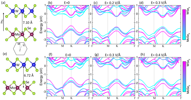
Theoretical model - In order to obtain the band structure and electron/hole distributions for the vdW heterostructure, DFT calculations were performed using the Vienna ab initio simulation package (VASP).VASP We used projector-augmented wave (PAW)PAW potentials and approximated the exchange-correlation potential with the Perdew-Burke-Ernzerhof (PBE)PBE functionals. Van der Waals corrections Grimmes and spin-orbit coupling were included in the calculations. During the ionic relaxation, the Brillouin zone of the unit cell was sampled by a grid of k-points. A plane-wave basis set with energy cutoff of 400 eV was used in all calculations. A large out-of-plane supercell size of 36 Å was chosen to ensure no interaction between adjacent supercells. While applying external electric field, dipole corrections were applied in order to remove spurious dipole interactions. Makov
In general, TMDCs bilayers are shown to be indirect gap semiconductors. Ganatra ; Mak However, vdW heterostructures with AA stacking, instead of the natural AB form, exhibit direct gap at K. Lin Electronically, these two layers are largely decoupled, with superposition of their monolayers bandstructure. Alternatively, AA’ stacked bilayers, namely, with transition metal atoms of one layer superposing chalcogen atoms of the other layer, also share the same qualitative features. In our calculations, the geometry of AA and AA’ stacked MoSe2/WSe2 supercells was first optimized at zero electric field, leading to the crystal structures shown in Figs. 1(a) and 1(e). For any other value of perpendicular electric field, we computed the optimum interlayer distance, by allowing the ions to relax in the out-of-plane direction until the atomic forces on the unit cell were less than 0.01 eV/Å . The charge density was computed by refining the solution to the Kohn-Sham equations with an energy convergence value of eV. While the above calculations were performed in the absence of spin-orbit coupling, a final run including spin-orbit coupling was used to compute wave functions and energy bands. Energies were calculated along the symmetry lines of the Brillouin zone shown in the inset of Fig. 1(a). Energies in all DFT results throughout the paper are shown using vacuum energy at zero electric field as reference.
From the pseudo-wave function of a specific band and -point (in what follows, we choose either or ), we extracted the probability function projection Proj to the bottom layer (MoSe2) as
| (1) |
and similarly (but integrating from to ) for the top layer (WSe2)
| (2) |
where stands for the two-dimensional Wigner-Seitz cell, and are the supercell lower and upper boundaries in the out-of-plane direction, respectively, and is the mid-point position between the two layers.
We define the exciton wave function, within the Wannier-Mott model, as , for electron and hole in the -th and -th layers, respectively. The exciton Hamiltonian in this basis reads
| (3) |
where stands for the bottom (top) layer and is the reduced effective mass for an electron (hole) in the -th layer. The exciton binding energy can then be obtained from , which leads to
| (4) |
where , and is the energy obtained by numerically solving Schrödinger equation for the in-plane motion considering as the electron-hole interaction potential. The latter is obtained from the quantum electrostatic heterostructure model, Thygesen assuming an electron in the -th layer and a hole in the -th layer. is calculated by first integrating the square modulus of the DFT obtained electron (hole) wave function in the surroundings of the ()-th layer (i.e. around and for bottom and top layers, respectively), such as in Eqs. (1) and (2), in order to obtain the contribution from each layer to the overall probability density distribution. Multiplying the results for electrons and holes yields the probability of simultaneously having an electron in and a hole in , namely , where () stands for the lowest (highest) conduction (valence) band states. In this way, the electron-hole overlap is given the probability of having both quasi-particles at layer 1 or layer 2, i.e. .
Results - DFT results in Figs. 1(b-d) and 1(f-h) show that the MoSe2/WSe2 heterostructure is a direct gap semiconductor at K point under all values of applied electric field investigated here, for both stacking configurations. Figures 1(b) and 1(f) show the band structure of the AA and AA’ stacked heterostructures at zero electric field. In both cases, from the color scale, one verifies that the wave functions at the K point are well localized in either the MoSe2 or WSe2 layer. Hence, the combined band diagram of the heterostructure preserves the properties of the band structure of its constituent monolayers. This observation supports the idea of using the layer-localized states () as a basis in which the Hamiltonian in Eq. (3) becomes diagonal. Otherwise, non-zero off-diagonal (hopping) terms would produce energy bands with layer-delocalized electron and hole wave functions instead.
When a positive electric field is applied (see Fig. 1(a)), the bands around K with prevalent MoSe2 character shift to higher energies, while those with WSe2 character shift to lower energies, as one would expect if the band structures were uncoupled (see Fig. 1(c) and Fig. 1(d) at 0.2 and 0.3 V/Å , respectively). This eventually results in a band crossing, which occurs around 0.2 V/Å for both conduction and valence bands at K. The same situation holds for AA’ stacked heterostructures, as shown in Figs. 1(f-h), albeit at a higher crossover electric field of 0.3 V/Å instead. A similar effect is also discussed in Ref. [Kaxiras, ].
The situation is more complicated, however, for the point, where the valence band states have highly mixed projections. Despite the fact that the valence band maximum is at K, the satellite valley at is very close in energy and might be experimentally accessible as well. In fact, a recent PL experiment suggests the observation of an indirect exciton composed of an electron at K and a hole at in a similar heterostructure, namely MoS2/WSe2. Jens The hole wavefunction at the point is found to be naturally distributed across both layers, despite the type-II nature of the heterostructure, thus leading to a high electron-hole overlap and higher recombination rate, as we will discuss in greater detail further on.
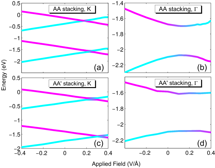
The energies of the two lowest conduction bands and the two highest valence bands at K point are plotted as a function of electric field in Fig. 2(a). It is clear that the band gap energy of the heterostructure can be modulated by the electric field, reaching its maximum value of 1.28 eV at 0.225 V/Å. Valence band extrema at the point are plotted as a function of the field in Fig. 2(b), where an important qualitative difference, as compared to the valence band at K, is evidenced: the bands crossing observed in K-point states for a field around 0.225 V/Å is replaced by an anti-crossing at 0.185 V/Å for the valence states. This suggest the existence of mixed layer states, namely, holes states at are delocalized across the two layers, in vicinity of the observed anti-crossing. Similar qualitative features are observed also in AA’ stacking case in Figs. 2(c) and 2(d). The intrinsic distribution of states in valence band over both layers is confirmed by the wave function calculations in what follows.
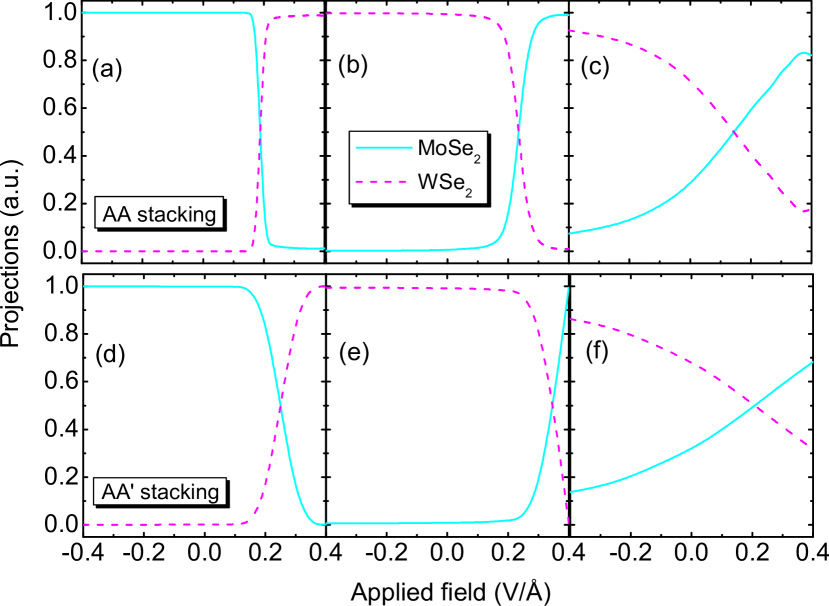
Wave function projections at K and points, calculated according to the definition in Eq. (1), are shown in Fig. 3 as a function of applied electric field. Figure 3(a) shows the projections of the lowest conduction band minimum (CBM) at K point, for AA stacking. For electric field values lower than 0.175 V/Å (including the negative values), the wave function is almost completely localized in the first layer (MoSe2). As the applied electric field increases, there is an abrupt shift to the other layer (WSe2). For the valence band maximum (VBM) at K, shown in Fig. 3(b), this trend is reversed, as expected from the type-II band alignment. Besides, the transition is smoother for VBM, indicating a more pronounced band mixing at the band crossing. As for the valence band states at point, shown in Fig. 3(c), the behavior is almost the same as for the hole states at K point, but there is an even smoother shift of wave functions from one layer to the other. We also note an intrinsic 65-35 distribution of this wave function between both layers, even in the absence of applied field. Similar results are also observed for the AA’ stacking case in Figs. 1(d-f), although the crossover occurs at a higher electric field, in accordance to the bands crossing shown in Fig. 2(c) and 2(d).
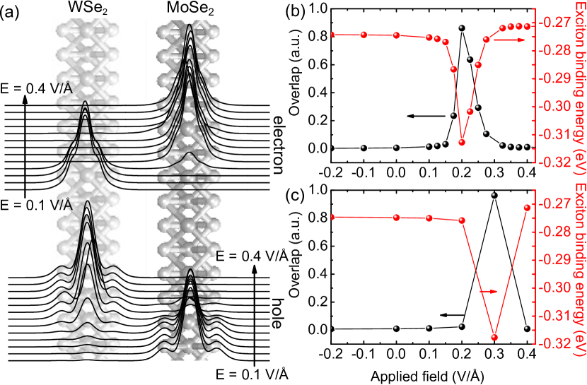
The DFT obtained electron and hole probability densities in the AA stacking case are illustrated in Figure 4(a), for different values of the perpendicularly applied electric field . It is clear that for low fields, electrons (holes) are strongly localized in the WSe2 (MoSe2) layer, as previously discussed. As the applied field becomes more positive, charge carriers are pushed towards the opposite layer, and the localization of these particles is interchanged. For intermediate values of the applied field, however, the wave functions partially populate both layers and, consequently, a stronger electron-hole population overlap is observed. This is verified in Fig. 4(b), for the AA stacked heterostructure, where this overlap reaches a maximum of 86 for V/Å , so that the modulus of the binding energy increases by 45 meV. Despite the strong enhancement of the overlap, the increase in binding energy is small because the combination of binding energies for each charge distribution case cannot be higher than the intra-layer values eV (WSe2) and eV (MoSe2). Inter-layer excitons have naturally lower binding energies eV and eV. The intensity (oscillator strength) of excitonic peaks (or its associated PL) is proportional to the square modulus of the exciton envelope wave function at , i.e. where electrons and holes are at the same point in space. Therefore, the electron-hole overlap is a measure of the exciton peak intensity and, consequently, the effects discussed here would manifest themselves in PL experiments as an inter-layer exciton peak whose spectral position and amplitude changes with external electric field. Results for the AA’ stacked case are shown in Fig. 4(c) and exhibit similar qualitative features, but with a 46 meV maximum variation of the exciton binding energy at V/Å , where the maximum overlap is 96, i.e. even higher than that of the AA stacked case.
Conclusion - We have investigated the exciton states in MoSe2/WSe2 heterostructures in the presence of an electric field applied perpendicularly to the layers. Our results show that for almost any value of electric field, this heterostructure clearly exhibits type-II band offsets for states around the K-point of the Brillouin zone. This can be inferred when both electron and hole wave functions are strongly localized in separate layers. However, at the crossover electric fields of around 0.2 (0.3) V/Å , for AA (AA’) stacking, charge carriers distributions are flipped. In the close vicinity of this crossover electric field, the charge densities (especially the one for holes) are distributed across both layers. In this case, the electron-hole overlap and, consequently, exciton binding energy and oscillator strength can be significantly enhanced.
The possibility of tuning the exciton binding energy and its PL emission intensity using an applied field opens an interesting avenue towards the search and enhancement of inter-layer charge-separated exciton states, whose experimental observation has proved to be elusive.
Acknowledgements.
Discussions with J. Kunstman, D. R. Reichman, and C. W. Wong are gratefully acknowledged. AC has been financially supported by CNPq, through the PRONEX/FUNCAP and PQ programs. JA and TL acknowledge support from NSF ECCS-1542202. We acknowledge computational support from the Minnesota Supercomputing Institute (MSI).References
- (1) K. F. Mak, C. Lee, J. Hone, J. Shan, and T. F. Heinz, Phys. Rev. Lett. 105, 136805 (2010).
- (2) R. Ganatra and Q. Zhang, ACS Nano 8,4074 (2014).
- (3) Y. Sun, D. Wang, and Z. Shuai, J. Phys. Chem. C 120, 21866 (2016).
- (4) Y. Zhang, T.-R. Chang, B. Zhou, Y.-T. Cui, H. Yan, Z. Liu, F. Schmitt, J. Lee, R. Moore, Y. Chen, H. Lin, H.-T. Jeng, S.-K. Mo, Z. Hussain, A. Bansil, and Z.-X. Shen, Nature Nano. 9, 111 (2014).
- (5) J. K. Ellis, M. J. Lucero, and G. E. Scuseria, Appl. Phys. Lett. 99, 261908 (2011).
- (6) T. Cheiwchanchamnangij and W. R. L. Lambrecht, Phys. Rev. B 85, 205302 (2012).
- (7) A. Kumar and P. K. Ahluwalia, Eur. Phys. J. B 85, 186 (2012).
- (8) P. Avouris, T. F. Heinz, and T. Low (editors), 2D Materials (Cambridge University Press, 2017).
- (9) Tony Low, Andrey Chaves, Joshua D. Caldwell, Anshuman Kumar, Nicholas X. Fang, Phaedon Avouris, Tony F. Heinz, Francisco Guinea, Luis Martin-Moreno, and Frank Koppens, Nat. Mat.16, 182 (2017).
- (10) Z. Ye, Ting Cao, Kevin O’Brien, Hanyu Zhu, Xiaobo Yin, Yuan Wang, Steven G. Louie, and Xiang Zhang, Nature 513, 214 (2014).
- (11) B. Zhu, et al., Sci. Rep. 5, 9218 (2015).
- (12) Miguel M. Ugeda, Aaron J. Bradley, Su-Fei Shi, Felipe H. da Jornada, Yi Zhang, Diana Y. Qiu, Wei Ruan, Sung-Kwan Mo, Zahid Hussain, Zhi-Xun Shen, Feng Wang, Steven G. Louie, and Michael F. Crommie, Nat. Mat. 13, 1091 (2014).
- (13) S. Tongay, et al., Nat. Comm. 5, 3252 (2014).
- (14) O. B. Aslan, et al., ACS Photonics 3, 96 (2016).
- (15) Alexey Chernikov, Timothy C. Berkelbach, Heather M. Hill, Albert Rigosi, Yilei Li, Ozgur Burak Aslan, David R. Reichman, Mark S. Hybertsen, and Tony F. Heinz, Phys. Rev. Lett. 113, 076802 (2014).
- (16) K. He, Nardeep Kumar, Liang Zhao, Zefang Wang, Kin Fai Mak, Hui Zhao, and Jie Shan, Phys. Rev. Lett. 113, 026803 (2014).
- (17) Edbert J. Sie, Alex J. Frenzel, Yi-Hsien Lee, Jing Kong, and Nuh Gedik, Phys. Rev. B 92, 125417 (2015).
- (18) J. S. Ross, et al., Nat. Comm. 4, 1474 (2012).
- (19) G. Wang, X. Marie, I. Gerber, T. Amand, D. Lagarde, L. Bouet, M. Vidal, A. Balocchi, and B. Urbaszek, Phys. Rev. Lett. 114, 097403 (2015).
- (20) B. Miller, Alexander Steinhoff, Borja Pano, Julian Klein, Frank Jahnke, Alexander Holleitner, and Ursula Wurstbauer, Nano Lett., Article ASAP (2017).
- (21) P. Rivera, J. R. Schaibley, A. M. Jones, J. S. Ross, S. Wu, G. Aivazian, P. Klement, K. Seyler, G. Clark, N. J. Ghimire, J. Yan, D. G. Mandrus, W. Yao, and X. Xu, Nature Communications 6, 6242 (2015).
- (22) Albert F. Rigosi, Heather M. Hill, Yilei Li, Alexey Chernikov, and Tony F. Heinz, Nano Lett. 15, 5033 (2015).
- (23) Hui Fang, Corsin Battaglia, Carlo Carraro, Slavomir Nemsak, Burak Ozdol, Jeong Seuk Kang, Hans A. Bechtel, Sujay B. Desai, Florian Kronast, Ahmet A. Unal, Giuseppina Conti, Catherine Conlon, Gunnar K. Palsson, Michael C. Martin, Andrew M. Minor, Charles S. Fadley, Eli Yablonovitch, Roya Maboudian, and Ali Javey, PNAS 111, 6198 (2014).
- (24) Y. Gong, S. Lei, G. Ye, B. Li, Y. He, K. Keyshar, X. Zhang, Q. Wang, J. Lou, Z. Liu, R. Vajtai, W. Zhou, and P. M. Ajayan, Nano Lett. 15, 6135 (2015).
- (25) Y.-C. Lin, R. K. Ghosh, R. Addou, N. Lu, S. M. Eichfeld, H. Zhu, M.-Y. Li, X. Peng, M. J. Kim, L.-J. Li, R. M. Wallace, S. Datta, and J. A. Robinson, Nature Comm. 6, 7311 (2015).
- (26) S. Pak et al., Nano Lett., Article ASAP (2017).
- (27) V. O. Özçelik, J. G. Azadani, C. Yang, S. J. Koester, and T. Low, Phys. Rev. B. 94, 035125 (2016).
- (28) C.-H. Lee, et al., Nat. Nanotech. 9, 676 (2014).
- (29) Timothy C. Berkelbach, Mark S. Hybertsen, and David R. Reichman, Phys. Rev. B 88, 045318 (2013).
- (30) S. Latini, T. Olsen, and K. S. Thygesen, Phys. Rev. B 92, 245123 (2015).
- (31) G. Kresse and J. Furthmuller, Phys. Rev. B 54, 11169 (1996).
- (32) P. E. Blochl, Phys. Rev. B 50, 17953 (1994).
- (33) J. P. Perdew, K. Burke, and M. Ernzerhof, Phys. Rev. Lett. 77, 3865 (1996).
- (34) S. Grimme, J. Comput. Chem. 27, 1787 (2006).
- (35) G. Makov and M. C. Payne, Phys. Rev. B 51, 4014 (1995).
- (36) R. M. Feenstra, N. Srivastava, Qin Gao, M. Widom, Bogdan Diaconescu, Taisuke Ohta, G. L. Kellogg, J. T. Robinson, and I. V. Vlassiouk, Phys. Rev. B 87, 041406(R) (2013).
- (37) K. Andersen, S. Latini and K. Thygesen, Nano Lett. 15, 4616 (2015).
- (38) D. Huang and E. Kaxiras, Phys. Rev. B 94, 241303(R) (2016).
- (39) J. Kunstmann, F. Mooshammer, P. Nagler, A. Chaves, F. Stein, N. Paradiso, G. Plechinger, C. Strunk, C. Schüller, G. Seifert, D. R. Reichman, T. Korn, k-space indirect interlayer excitons in MoS2/WSe2 van der Waals heterostructures, submitted (2017).