The SPEDE spectrometer
Abstract
The electron spectrometer, spede, has been developed and will be employed in conjunction with the Miniball spectrometer at the HIE-ISOLDE facility, CERN. spede allows for direct measurement of internal conversion electrons emitted in-flight, without employing magnetic fields to transport or momentum filter the electrons. Together with the Miniball spectrometer, it enables simultaneous observation of rays and conversion electrons in Coulomb-excitation experiments using radioactive ion beams.
1 Introduction
In-beam spectroscopic methods have extensively been employed to uncover the governing forces in atomic nuclei. The outcome of the development of detector materials and detection techniques has culminated in large -ray detector arrays and various electron spectrometers (see e.g. References Akkoyun2012AGATAArray ; Eberth2008FromDetectors ; VanKlinken1975Mini-orangeElectrons ; Butler1996 and references therein). In order to establish a complete picture of de-excitation processes in a single experiment, simultaneous observation of all de-excitation paths is required. The combination of efficient detection of both rays and conversion electrons, as demonstrated by the sage spectrometer Pakarinen2014 , can be considered as one of the latest milestones in in-beam spectroscopy. The advent of radioactive beam facilities, such as the recently commissioned HIE-ISOLDE post-accelerator at CERN Rodriguez2016FirstHIE-Isolde , have allowed for multi-step Coulomb-excitation experiments employing radioactive ion beams to be performed. For the analysis of Coulomb-excitation data it is of particular importance to obtain complementary spectroscopic information, e.g. electron conversion coefficients Zielinska2016AnalysisCode . In this paper a compact SPectrometer for Electron DEtection (spede), which will be combined with the Miniball spectrometer Warr2013 at HIE-ISOLDE, is described.
2 The spede conversion electron spectrometer
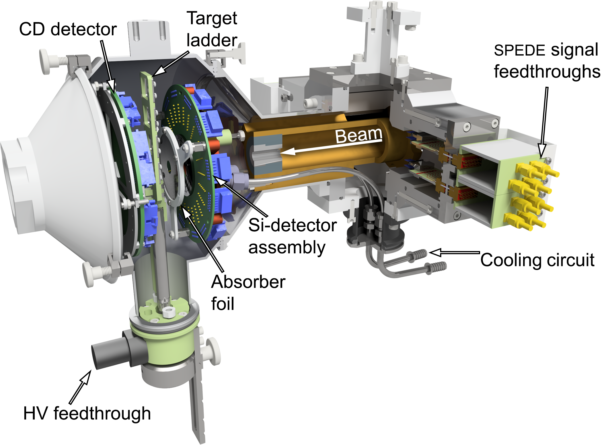
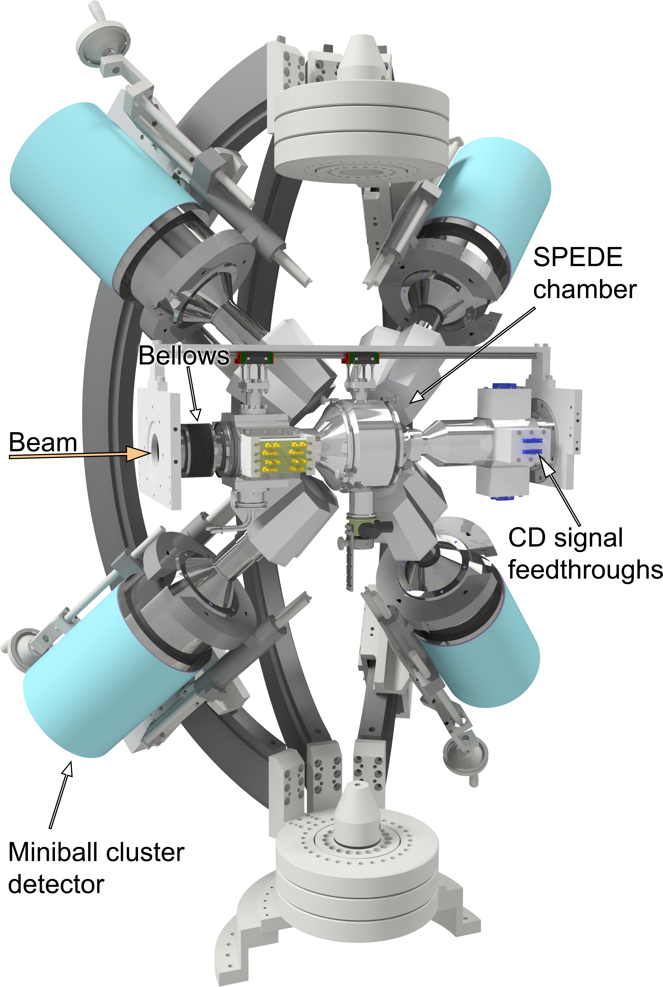
The features of spede and its compatibility with the Miniball spectrometer are described in the following subsections. Shown in Figure 1 is spede including the Miniball particle detector for Coulomb-excitation experiments, a double-sided silicon strip detector (CD detector) Ostrowski2002 . The development of spede has been discussed in detail in References Konki2013 ; Papadakis2015 ; Cox2017 .
2.1 Si-detector assembly
spede utilises a 24-fold segmented annular Si detector for the detection of internal conversion electrons. The detector is placed upstream and at a variable distance from the target. The conceptual design of spede and the suppression of the -electron background, discussed in more details in Subsection 2.2, assure that the conversion-electron signals are not overwhelmed by the high background. This allows for the placement of the detector in close proximity to the target, typically at a distance of 25 mm, providing large angular coverage and detection efficiency of the order of 8 across a wide energy range. In Coulomb-excitation experiments the direct observation of electrons, i.e., without the use of magnetic fields for electron transportation, is essential for the kinematic correction of their velocities. To correct for the velocity, the angle between the detected electron and electron-emitting scattered particle is required. This can be obtained by using the spede detector for the detection of electrons and the CD detector for the identification of scattered beam- and target-like particles, with the required angular, energy and time resolution.
A 17 mm aperture in the centre of the detector allows for the beam to pass through before impinging on the target. The 24 detector segments are arranged in three concentric rings around the beam aperture with 8 segments each. The segmentation scheme was optimised to provide sufficient position resolution for kinematic correction of the observed electron energies, while keeping the number of electronics channels relatively low Konki2013 . The widths of the segments (5.2, 3.9 and 3.2 mm, from the innermost) were chosen so that their individual surface areas are kept approximately equal in order to keep the capacitance the same across all segments. The intersegment gaps are 0.05 mm wide leading to a total detector inactive area of less than 2. The detector incorporates inner and outer guard rings to guarantee a homogeneous potential across the active area and minimise edge effects, also the bonding pads are distributed around the outer edge of the detector. A photograph of the detector mounted on the Printed Circuit Board (PCB) is presented in Figure 2 together with the detector geometry. The thickness of the detector presented here is 500 m and is optimised for electron energies up to 400 keV. Detectors with a thickness of up to 1500 m can be produced.
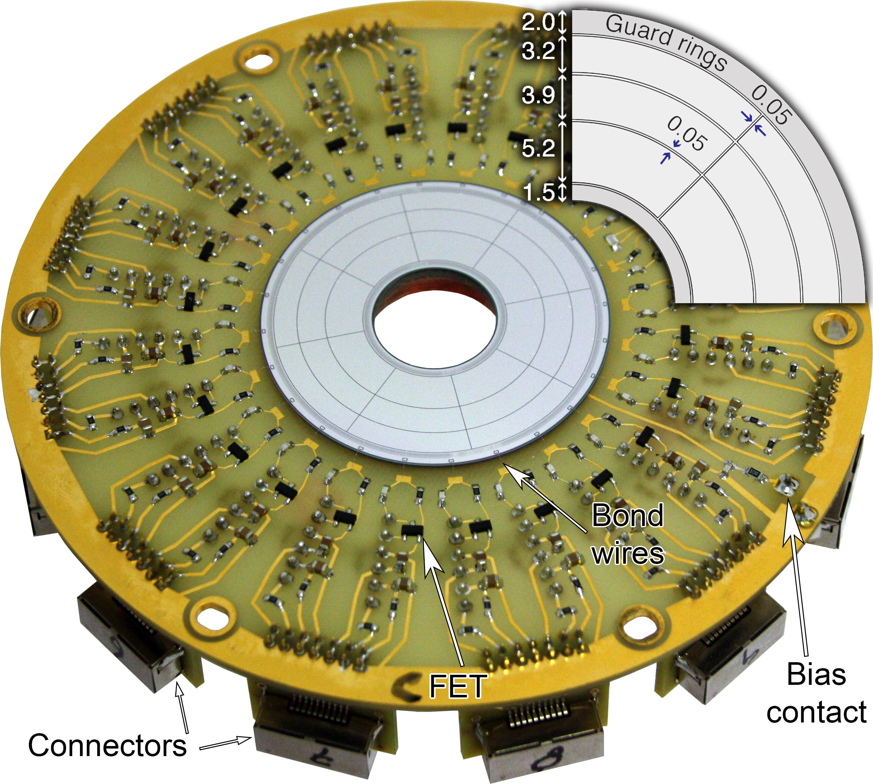
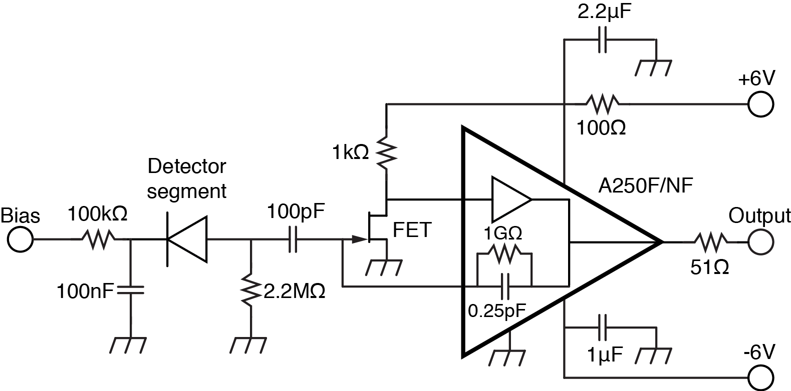
Each detector segment is connected to an AMPTEK A250F/NF charge-sensitive preamplifier through a PMBF4393 surface mount field effect transistor (FET). The gain of the preamplifiers is 4 V/pC, equivalent to 175 mV/MeV. Both the FETs and preamplifiers are positioned on the detector PCB inside the vacuum chamber. The preamplifier requires 6 V, which is filtered by dedicated circuits on the PCB. The bias voltage is supplied on the rear common cathode of the detector through a 100 k bias resistor, which is decoupled to ground through a 100 nF capacitor. The bias voltage for a detector of thickness 500 m is 90 V and the leakage current at the operating temperature is less than 1 nA. The preamplifiers are AC coupled to the detector segments through 100 pF capacitors. A 2.2 M resistor is connected to each individual segment to act as the return path for the current from the detector. Due to the output drive limitations of the preamplifiers a 51 resistor was added in series with each output to prevent preamplifier loading and to back terminate the 50 cable impedance. The circuit diagram for a single detector segment is presented in Figure 3.
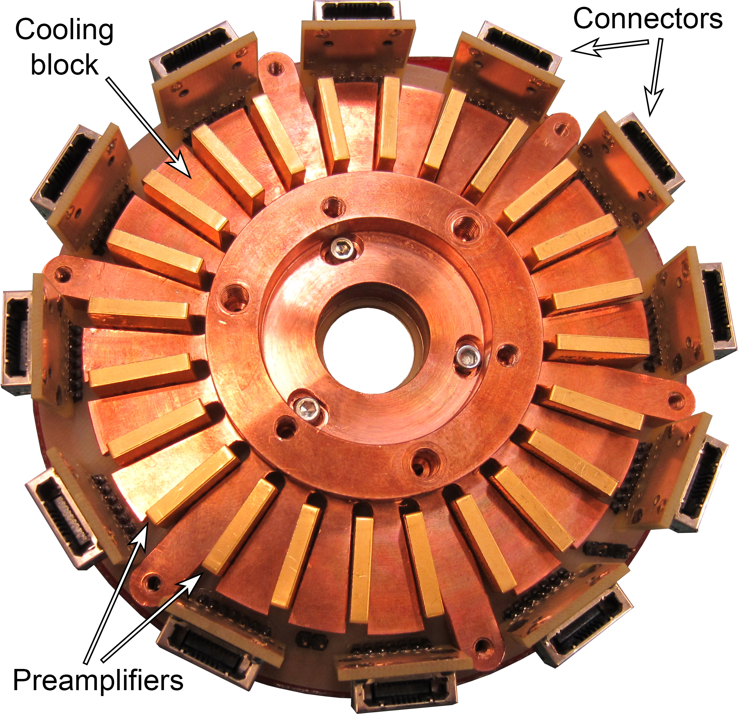
Two electronics channels are attached to each connector shown in Figures 2 and 4. Micro-coaxial cable assemblies transport the signal from the connectors to the signal feedthroughs shown in Figure 1. These assemblies also contain the preamplifier power cables.
To increase the stability of the Si detector and reduce electronic noise, the detector and preamplifiers are cooled. The detector PCB is mounted on a copper block housing an ethanol cooling circuit, that also integrates a fan-like structure surrounding the individual preamplifiers. The ethanol is circulated by a Julabo CF40 cryo-compact circulator with factory specified temperature range between -40∘C and +150∘C and cooling capacity of 0.12 kW at -30∘C. During normal operating conditions the detector temperature is in the region of -5∘C to 0∘C.
2.2 Suppression of electron background
Conventionally, electron spectrometers have employed magnetic fields to transport electrons away from the vicinity of the production target. Consequently, magnetic lenses Kantele1975ASelection or high-voltage barriers Butler1996 have been re becausequired to suppress the overwhelming -electron background produced in the collisions between fast, heavy ions and target atoms. The fact that spede is operated with low-intensity radioactive ion beams already reduces the -electron rate compared to in-beam experiments with stable-ion beams of higher intensity. Segmenting the detector into 24 pixels further reduces the -electron rate per channel. In addition, the following measures have been utilised to reduce the -electron background in spede.
2.2.1 Detection geometry
The spede detector is positioned upstream of the target because electrons are primarily forward focused and the flux at backwards angles is lower by several orders of magnitude Bechthold1997 . An additional benefit of this detection geometry is the reduction of kinematic broadening, which is lowest when the trajectories of the electron-emitting particle and the electron are collinear.
2.2.2 Introduction of high voltage on the target
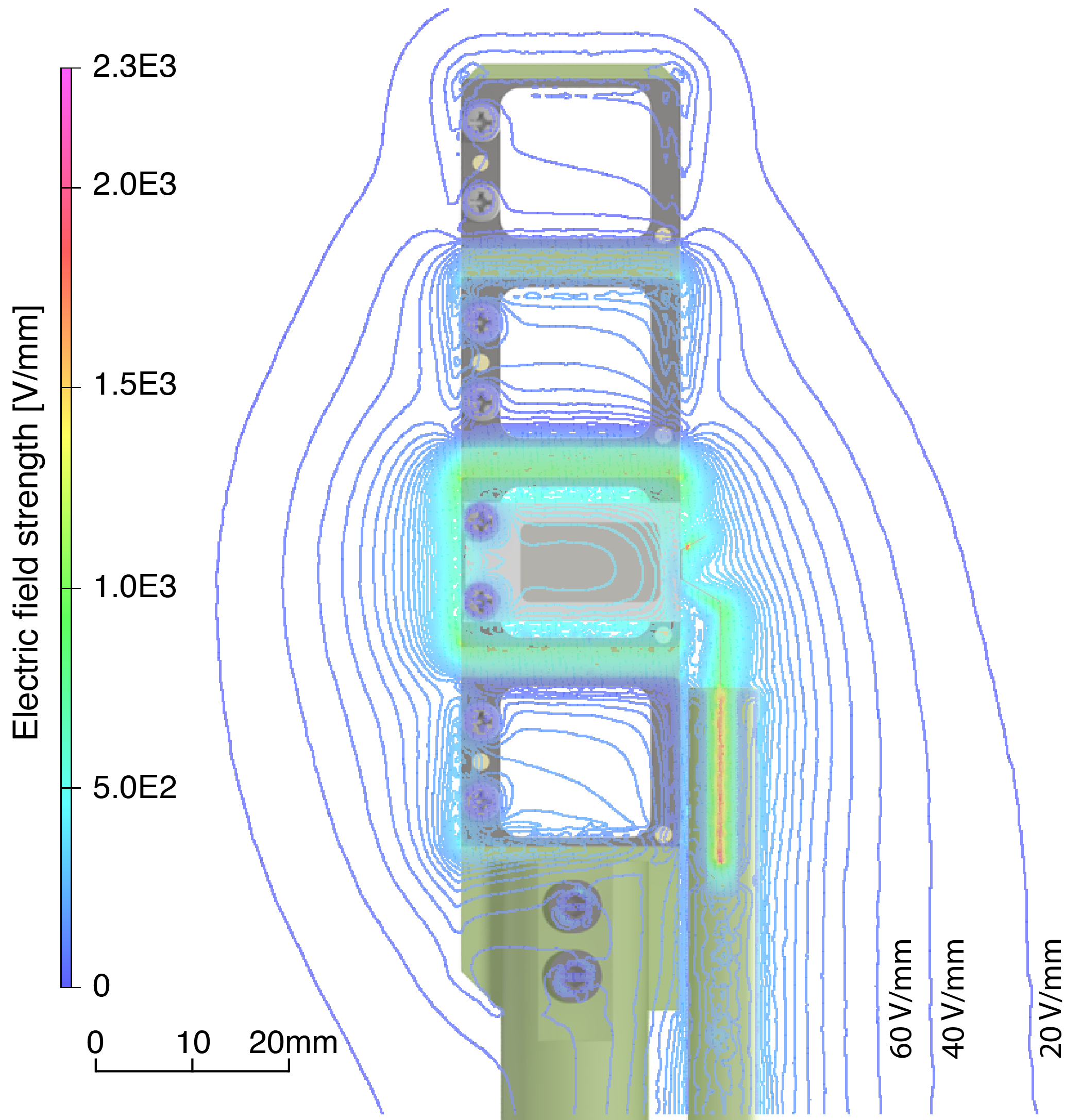
spede utilises a target ladder with four target positions, interchangeable from outside of the vacuum chamber. The majority of the -electron flux is concentrated below 5 keV Bechthold1997 . For this reason high voltages up to +5 kV may be applied to the target in use. The high voltage decelerates the emitted electrons and reduces the number of low-energy electrons reaching the spede detector. To ensure application of the voltage only on the target in use, the target ladder is made of insulating PEEK plastic, with metal inserts for mounting the targets and applying voltage. Contact is made through a spring arm with the in-beam target mounting frame, thus ensuring that the target integrity is not compromised. The remaining target frames may either be left floating or grounded through similar spring arm contacts.
The electric field profile at the target was simulated using the opera 3d simulation package Fields . These simulations were used in designing the target ladder to avoid regions of high electric field density which might lead to high-voltage discharges. All components in close proximity to the target were included in the simulation. Figure 5 shows the target ladder geometry overlaid with the simulated electric field strength. The electric field profile was also included in the Geant4 Agostinelli2003 simulations presented later in this paper.
2.2.3 Absorber foil
An aluminised Mylar foil is positioned between the target and the spede detector to absorb low-energy electrons which escape the target. Any material in the path of the electrons affects the efficiency and effective resolution of the detector, thus, the absorber foil thickness is chosen to balance requirements of both suppression and resolution. The results presented in this paper were obtained using a 12 m (1.68 mg/cm2) Mylar foil with 0.5 m (0.14 mg/cm2) aluminium deposited on the surface.
In order to obtain additional shielding against external noise, the aluminised Mylar foil is kept at ground potential. Moreover, the opaque nature of the foil in combination with a plastic ring covering the area between the detector and foil acts as a shield against the possible fluorescence light emitted from certain target materials.
2.2.4 Suppression of random -decay background
Background of random -decay origin will be suppressed by requiring a coincidence between the detected electrons in the spede detector and the scattered particle observed in the CD detector. After a coincidence condition is applied, particles will be typically included only as random correlations, thus the background of -decay origin should be suppressed significantly.
2.2.5 Effect of the high voltage and absorber foil on spectral quality
The effects of the high voltage and the absorber foil are shown individually in Figure 6. A -5 keV shift in the electron peak positions and no obvious change to the electron resolution are evident in the spectrum with high voltage. In the spectrum with absorber foil the electrons are shifted towards lower energies and the resolution is degraded due to straggling in the foil. This is more prominent for the lower-energy electrons. Indicative values of the effects of the high voltage and absorber foil at electron energies of 75 keV and 320 keV are presented in Table 1.
| Energy | FWHM | Energy | FWHM | |
|---|---|---|---|---|
| [keV] | [keV] | [keV] | [keV] | |
| Literature | 75.28(1) | 320.03(1) | ||
| This work | ||||
| Unsuppressed | 75.4(1) | 9.7(1) | 320.2(1) | 6.6(1) |
| +5 kV | 70.0(1) | 9.6(1) | 315.2(1) | 6.9(1) |
| Absorber foil | 63.6(1) | 12.9(1) | 316.0(1) | 7.7(1) |
The effect of the background suppression methods on the peak-to-total value (P/T) was investigated using a 133Ba source with a low-energy cut at 50 keV. The spectrum with +5 kV high voltage is of similar quality to the unsuppressed (P/T of 0.58(5)), whereas the spectral quality is reduced for the case where the aluminised Mylar foil is used (P/T of 0.41(5)).
2.3 Electron detection efficiency
The relative detection efficiency of spede was determined using open 133Ba and 207Bi calibration sources. The relative efficiency values were normalised to a simulated efficiency curve produced using Geant4. The measured efficiency and simulated efficiency curve are presented in Figure 7. The sources were mounted on the target ladder and no voltage or absorber foil were used. The simulation package has been developed within the nptool framework Matta2016 and will be presented in more detail elsewhere Cox . It contains the full Miniball spectrometer, the complete geometry of spede, including the support structures, absorber foil and electric field produced by the high voltage applied to the target. To allow for comparison between the different set-ups the Miniball Coulomb-excitation target chamberWarr2013 has also been included.
The detection efficiency remains relatively constant for energies up to 400 keV and close to the expected value calculated from geometrical constraints. At higher energies the detection efficiency decreases as the number of punch-through events and electrons not depositing their full energy in a single segment increases. For detection of higher-energy electrons a thicker detector could be used. For comparison the simulated efficiency curve with a 1000 m detector is also plotted in Figure 7. The efficiency in the region of 1 MeV is increased by a factor of 7, while the efficiency below 400 keV remains largely unaffected. The aluminised Mylar absorber foil used for the results presented in this paper reduces the efficiency below 150 keV, but does not have a significant effect at higher electron energies.
2.4 Combining with Miniball
spede was designed to be compatible with the existing Miniball infrastructure at HIE-ISOLDE, CERN. spede in the centre of Miniball spectrometer is shown in Figure 8.
A compact aluminium target chamber with 2.5 mm thick walls houses the spede detector, target ladder and the CD detector. The beam pipe and CD-detector feedthroughs of the Miniball Coulomb-excitation target chamber are connected to the downstream part of the spede chamber, while the CD detector is mounted on a purpose-built support. A beam pipe accommodating the spede detector feedthroughs is connected upstream of the target chamber. This beam pipe includes the support structure for the spede detector, the beam collimator and the ethanol cooling circuit pipes (see Figure 1).
During operation the spede target ladder allows the use of any one of the four targets without opening the target chamber. Access to the spede or CD detector can be gained by removing the bellows (see Figure 8) and sliding the target chamber on a rail system in the upstream direction.
The design of the Miniball frame enables the placement of the cluster Ge detectors at various angles and rotations. This allows for the use of different target chambers and ancillary detectors without compromising the -ray detection efficiency.
3 Performance of spede
3.1 Simultaneous -ray and conversion-electron spectroscopy at HIE-ISOLDE
The integration of spede with the Miniball spectrometer was tested using an implanted radioactive 191Hg source. The decay chain 191Hg( 50 min) 191Au(2.2 h) 191Pt (2.8 d) provided a high-statistics data set to perform simultaneous -ray and conversion-electron (e)spectroscopy. This is illustrated in panel a) of Figure 9, where the total singles -ray energy spectrum obtained with the aforementioned source is shown. Panel b) of Figure 9 shows the total singles electron energy spectrum and electrons in coincidence with any ray. It should be noted that the electron energy spectra include background arising from the decay of 191Hg Baglin2009Nuclear179 . The e performance is demonstrated in Figures 9 c) and d), where gates on the e matrix are set on the 586 keV ray and the 116 keV electron lines (corresponding to the K-electron line of the 194 keV transition in 191Pt), respectively.
3.2 In-beam testing of spede at JYFL-ACCLAB
The in-beam performance of spede has been investigated in a Coulomb-excitation experiment employing the82Kr(197Au,197Au*) reaction at 4.26 MeV/u beam energy in the Accelerator Laboratory of the University ofJyväskylä (JYFL-ACCLAB), first reported in Cox2017 . The target was a self-supporting 1200 g/cm2 thick gold foil. The beam from the K130 cyclotron was chopped to provide bunches of 200 s beam-on and 800 s beam-off to replicate the typical time structure of the HIE-ISOLDE beam. The performance of spede was tested up to pps impinging on the target. In typical running conditions the beam intensity was pps, resulting in an average counting rate of 1300 Hz/channel in the spede detector. Scattered particles were detected with an array of six 1 cm2 PIN diodes described in Cox2017 .
Figure 10 shows the measured and simulated particle-gated electron energy spectra. Both spectra are kinematically corrected for 197Au and were obtained using the aluminised Mylar absorber foil and no high voltage on the target. The simulated spectrum reproduces the main structures in the measured spectrum and the ratio between the detected peaks. The complexity of the measured background makes its accurate simulation unrealistic and computationally demanding.
A K/L conversion ratio of 5.7(7) for the 279 keV transition in 197Au was extracted from the data shown in Figure 10 and using the efficiency presented in Figure 7. The value obtained is compared with the K/L ratios calculated using the BrIcc conversion coefficient calculator Kibedi2008 for pure M1 and E2 transitions and with a mixed M1+E2 transition using the mixing ratio of =-0.39(2) Stuchbery1988Measured197Au . The measured value is in excellent agreement with the calculated value for a mixed transition.
| M1 | E2 | M1+E2 | ||
| (BrICC) | (BrICC) | (literature) | This work | |
| K/L ratio | 6.05(12) | 1.85(4) | 5.63(13) | 5.7(7) |
4 Summary
spede has been built and commissioned at JYFL-ACCLAB and at the HIE-ISOLDE facility, CERN. spede combines a segmented Si detector for the measurement of internal conversion electrons directly from the target with the Miniball spectrometer for the measurement of rays and scattered particles. The off-line tests indicate that the spectrometer works within the design criteria with a detection efficiency of the order of 8 and FWHM at 320 keV in the region of 6-8 keV depending on the running conditions. The first in-beam tests have shown the power of the spectrometer for the direct detection of conversion electrons and the extraction of conversion coefficients. A comprehensive simulation package for the set-up was developed using the nptool framework in Geant4 and can be used to investigate the feasibility of planned experiments.
We would like to acknowledge Magdalena Zielińska Jose Alberto Rodriguez, Miguel Lozano Benito and Karl Johnston for their help and support during the tests at ISOLDE. The research leading to these results has received funding from the People Programme (Marie Curie Actions) of the European Union’s Seventh Framework Programme (FP7/2007-2013) under REA grant agreement n∘ 304033, by the Academy of Finland (contract number 265023) and by the United Kingdom Science and Technology Facilities Council (Grant Ref. ST/J000094/1). The Miniball collaboration is acknowledged for supporting this project. In addition, the German BMBF under contracts 05P15RDCIA and 05P15PKCIA and ”Verbundprojekt 05P2015” are acknowledged.
References
- (1) S. Akkoyun et al., Nuclear Instruments and Methods in Physics Research, Section A: Accelerators, Spectrometers, Detectors and Associated Equipment 668, 26 (2012), ISSN 01689002, DOI 10.1016/j.nima.2011.11.081
- (2) J. Eberth, J. Simpson, Progress in Particle and Nuclear Physics 60(2), 283 (2008), ISSN 01466410, DOI 10.1016/j.ppnp.2007.09.001
- (3) J. Van Klinken et al., Nuclear Instruments and Methods 130(2), 427 (1975), ISSN 0029554X, DOI 10.1016/0029-554X(75)90040-3
- (4) P.A. Butler et al., Nuclear Instruments and Methods in Physics Research Section A 381(2-3), 433 (1996), ISSN 01689002, DOI 10.1016/S0168-9002(96)00762-0
- (5) J. Pakarinen et al., The European Physical Journal A 50(3), 53 (2014), ISSN 1434-6001, DOI 10.1140/epja/i2014-14053-6
- (6) J.A. Rodriguez et al., Proceedings of IPAC2016 pp. 1284–1286 (2016), DOI 10.18429/JACoW-IPAC2016-TUPMR023
- (7) M. Zielińska et al., European Physical Journal A (2016), ISSN 1434601X, DOI 10.1140/epja/i2016-16099-8
- (8) N. Warr et al., European Physical Journal A 49(3), 1 (2013), ISSN 14346001, DOI 10.1140/epja/i2013-13040-9
- (9) A. Ostrowski et al., Nuclear Instruments and Methods in Physics Research Section A: Accelerators, Spectrometers, Detectors and Associated Equipment 480(2), 448 (2002), ISSN 01689002, DOI 10.1016/S0168-9002(01)00954-8
- (10) J. Konki et al., EPJ Web of Conferences 63, 01019 (2013), ISSN 2100-014X, DOI 10.1051/epjconf/20136301019
- (11) P. Papadakis et al., in Proceedings of the Conference on Advances in Radioactive Isotope Science (ARIS2014) (Journal of the Physical Society of Japan, 2015), Vol. 030023, pp. 4–7, DOI 10.7566/JPSCP.6.030023
- (12) D.M. Cox et al., Acta Physica Polonica B 48(3), 403 (2017), DOI 10.5506/APhysPolB.48.403
- (13) J. Kantele et al., Nuclear Inst. and Methods in Physics 130(2), 467 (1975)
- (14) U. Bechthold et al., Physical Review Letters 79(11), 2034 (1997), ISSN 0031-9007, DOI 10.1103/PhysRevLett.79.2034
- (15) Vector Fields ”OPERA Version 12” (2007), www.vectorfields.com
- (16) S. Agostinelli et al., Nuclear instruments & methods in physics research. Section A, Accelerators, spectrometers, detectors and associated equipment 506(3), 250 (2003), ISSN 01689002, DOI 10.1016/S0168-9002(03)01368-8
- (17) Y. Khazov, A. Rodionov, F.G. Kondev, Nuclear Data Sheets 112, 855 (2009), ISSN 00903752, DOI 10.1016/j.nds.2009.06.002
- (18) A. Matta et al., Journal of Physics G: Nuclear and Particle Physics 43(4), 45113 (2016), ISSN 0954-3899, DOI 10.1088/0954-3899/43/4/045113
- (19) D.M. Cox, To Be Published (2017)
- (20) C.M. Baglin, Nuclear Data Sheets 110(2), 265 (2009), ISSN 00903752, DOI 10.1016/j.nds.2009.01.001
- (21) A. Johansson et al., Nuclear Physics A98, 278 (1978)
- (22) T. Kibédi et al., Nuclear instruments & methods in physics research. Section A, Accelerators, spectrometers, detectors and associated equipment 589(2), 202 (2008), ISSN 01689002, DOI 10.1016/j.nima.2008.02.051
- (23) A.E. Stuchbery et al., Nuclear Physics 486, 374 (1988)