Tunable Anomalous Andreev Reflection and Triplet Pairings in Spin Orbit Coupled Graphene
Abstract
We theoretically study scattering process and superconducting triplet correlations in a graphene junction comprised of ferromagnet-RSO-superconductor in which RSO stands for a region with Rashba spin orbit interaction. Our results reveal spin-polarized subgap transport through the system due to an anomalous equal-spin Andreev reflection in addition to conventional back scatterings. We calculate equal- and opposite-spin pair correlations near the F-RSO interface and demonstrate direct link of the anomalous Andreev reflection and equal-spin pairings arised due to the proximity effect in the presence of RSO interaction. Moreover, we show that the amplitude of anomalous Andreev reflection, and thus the triplet pairings, are experimentally controllable when incorporating the influences of both tunable strain and Fermi level in the nonsuperconducting region. Our findings can be confirmed by a conductance spectroscopy experiment and provide better insights into the proximity-induced RSO coupling in graphene layers reported in recent experiments avsar2014nat, ; ex1, ; ex2, ; ex3, .
pacs:
72.80.Vp, 74.25.F-, 74.45.+c, 74.50.+r, 81.05.ueI introduction
Ferromagnetism and wave superconductivity are two phases of matter with incompatible order parameters. The interplay of superconductivity and ferromagnetism in a junction platform results in intriguing and peculiar phenomena Buzdin2005RMP ; eschrig_2015 ; bergeret_rmp . For instance, in a standard uniform superconductor-ferromagnet-superconductor (S-F-S) junction, supercurrent can go under multiple reversals when varying temperature, exchange field, and junction thickness Ryazanov2001PRL . These sign reversals are due to the apparence of triplet opposite-spin pairings (OSPs) and thus the oscillation of Cooper pairs’ amplitude in the time-reversal broken region i.e. F Buzdin2005RMP ; kupriyanov ; bergeret_rmp ; ma_jap . If magnetization in the F region follows a nonuniform pattern a new type of superconducting correlations arises: Triplet equal-spin pairings (ESPs). The equal-spin pair correlations are long range and can extensively propagate in materials with uniform magnetization and strong scattering resources Buzdin2005RMP ; eschrig_2015 ; bergeret_rmp ; ma_jap . This long range nature of spin-polarized superconducting correlations has turned the ESPs to a highly attractive perspective in nanoscale spintronics eschrig_2015 ; rob ; bob ; moor ; sat ; khay ; sac ; halfm . Another source to generate the ESPs is a combination of spin orbit interactions and uniform Zeeman field proximitized to a superconducting electrode Hogl2015PRL ; bergprb ; ma_jpc ; ma_njp . One of the main advantages of making use of spin orbit interactions to induce the ESPs is an all electrical control over the ESPs bobkova ; bergprb ; Hogl2015PRL ; Konschelle ; grigor ; ma_jpc ; ma_njp ; arijit .
Graphene is a single layer of carbon atoms, arranged in hexagonal lattices, with a linear dispersion at low energies and tunable Fermi level that can be simply manipulated by a gate voltage cast1 ; beenakkerrmp . These exceptional characteristics in addition to a long spin relaxation time of moving charged carriers, compared to their counterparts in a standard conductor, has turned graphene to a promising material for spintronics devices cast1 ; beenakkerrmp . Superconductivity, ferromagnetism, and spin orbit interactions can be induced into graphene layers by means of the proximity effect Heersche2007Nature ; Tombros2007Nature ; Chakraborty2007PRB ; Dedkov2008PRL ; Varykhalov2012PRL ; vahid ; rameshti ; ex1 ; ex2 ; ex3 ; avsar2014nat . It was experimentally demonstrated that a graphene monolayer can support strong Rashba spin orbit interaction of order of 17 meV by proximity to a semiconducting tungsten disulphide substrate avsar2014nat . Recent developments have achieved large proximity-induced ferromagnetism and spin orbit interactions in CVD grown graphene single layers coupled to an atomically flat yttrium iron garnet ex1 ; ex2 ; ex3 . To demonstrate the existence of proximity-induced RSO interaction in the graphene layer, a DC voltage along the graphene layer is measured by spin to charge current conversion which is interpreted as the inverse Rashba-Edelstein effect ex1 ; ex2 ; ex3 . The Edelstein effect was first discussed in connection with the spin polarization of conduction electrons in the presence of an electric current ed . Furthermore, graphene has the capability of sustaining strain and deformations without rupture Peres2010RMP ; Pereire2009PRB . The application of strain to graphene layers can result in important and interesting phenomena Jiang_strain ; Assili_strain1 ; Verbiest_strain1 ; Benjamin_strain1 ; Manes_strain ; Gruji_strain ; Wang_strain1 ; strain ; ramin ; sattari . For example, the interplay of massive electrons with spin orbit coupling in the presence of strain in a graphene layer yields controllable spatially separated spin-valley filtering Gruji_strain ; Jiang_strain . Therefore, this property can be employed as a means to control the spin-transport graphene-based spintronics devices ramin .
In this paper, we incorporate RSO interaction, superconductivity, ferromagnetism, and two different types of strain in a set up of graphene-based F-RSO-S contact (depicted in Fig. 1) and propose an experimentally feasible device to generate ‘controllable’ odd-frequency superconducting triplet correlations. Our results reveal a finite anomalous equal-spin Andreev reflection due to the RSO interaction. We demonstrate that this anomalous reflection results in nonvanishing superconducting ESPs in the ferromagnetic region near the F-RSO interface. We also vary the Fermi level (that can be experimentally achieved using a gate voltage) and the strength of an applied strain and show that by simply tuning these two physical quantities one can suppress the amplitude of opposite-spin superconducting correlations while simultaneously increase the equal-spin pairings at the F-RSO interface. Furthermore, we study the charge and spin conductances of the junction and show that the anomalous equal-spin Andreev reflection yields a finite tunable spin-polarized subgap conductance which is experimentally measurable. Such a spectroscopy experiment can be an alternative to those of Refs. avsar2014nat, ; ex1, ; ex2, ; ex3, for demonstrating the existence of proximity-induced RSO in graphene layers and determining its characteristics. We complement our findings by investigating the system’s band structure and discussing its aspects.
The paper is organized as follows. We first summarize the theoretical framework used in Sec. II. The results are discussed in Sec. III in three subsections: in Subsec. III.1 we study the band structure of system and discuss various reflection and transmission probabilities, in Subsec. III.2 the explored anomalous Andreev reflection is linked to the ESPs, and we study the spin and charge conductances in Subsec. III.3. More details of analytics and calculations are discussed in Appendix. We finally summarize concluding remarks in Sec. IV.
II formalism and theory
Because of the specific band shape of monolayer graphene in low energies, carriers in such a system can be treated as massless Dirac fermions cast1 . Thus, to describe the low-energy excitations of the structure shown in Fig. 1, one can incorporate the Dirac Hamiltonian with the Bogoilubov-de Gennes equation to reach at a Dirac-Bogoliubov-de Gennes (DBdG) equation in the presence of RSO coupling and exchange field as follow Beenakker :
| (1) |
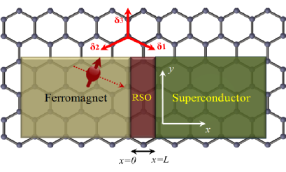
where is the quasiparticles’ energy and and refer to the electron and hole parts of spinors, respectively. is a two dimensional massless Dirac Hamiltonian which governs low energy excitations in one valley of graphene and is the time reversal operator beenakkerrmp . and are components of wave vector in the and directions, respectively. and are Pauli matrices, acting on the pseuedospin and real spin spaces of graphene ( and are unit matrices) and natural units are used: . The index labels F, RSO, or S regions as seen in Fig. 1:
| (2) |
where indicates the thickness of RSO region. Here is the energy scale of spin orbit coupling and is the electrostatic potential in the superconducting region. Because of valley degeneracy in a single layer of graphene, one can simply multiply final results by a factor of two. In a graphene layer under strain which implies anisotropic Fermi velocity in F, RSO, and S regions. The Fermi energy in each region is shown by . In the Hamiltonian of F segment, Eq.(2), represents the exchange field which is added to the Dirac Hamiltonian via the Stoner approach. For simplicity in our calculations, we assume that is oriented along the direction without loss of generality halt1 . This choice turns the exchange field to a good quantum number that allows for explicitly considering spin-up and -down quasiparticles in the F region and helps having insightful analyses of spin-dependent phenomena in the system. The superconducting gap is a matrix in the particle-hole space (nonzero in ) and is given by:
| (3) |
in which is the superconducting gap at zero temperature, is the macroscopic phase of superconductor, and denotes a Heaviside step function. This step function assumption made is valid as far as the Fermi wavelength in the S region is much smaller than F and RSO regions i.e. . Otherwise, a self-consistent approach is favorable to accurately determine the spatial profile of the pair potential halt_2011 ; halt1 . We also assume that the F-RSO junction can be described by a step change from the ferromagnetic region to RSO. Although we initially do not consider a smooth change at this junction (that can happen in realistic systems due to the proximity effect), each region eventually gains its own neighbour properties near the boundary by matching their wavefunctions at this location beenakkerrmp . We note that such modifications, including weak nonmagnetic impurities and moderately rough interfaces, can only alter the amplitude of scattering probabilities and not the conclusions of our work.
To describe a strained graphene layer, we follow Ref. Pereire2009PRB, . Expanding the tight-binding model band structure with arbitrary hopping energies around the Dirac point, one finds:
| (4) |
where is the lattice vector as depicted in Fig. 1. The position of one of the Dirac points is . Here, we assume , and in our calculations (see Ref. Alidoust2011, ). These assumptions constitute asymmetric velocities to the Dirac fermions in different directions.
To satisfy the mean field approximation in the S region (which is experimentally relevant) namely, the Fermi wavevector in the superconductor should be much larger than its F and RSO counterparts beenakkerrmp , we consider a heavily dopped superconductor, that is achieved by Beenakker . The resulting wavefunctions are spinors (see Appendix). We match these wavefunctions at the boundaries i.e. at and and calculate various probabilities of the electron-hole scatterings. We normalize energies by the superconducting gap at zero temperature and lengths by the superconducting coherent length . The gap of superconductor depends on the temperature () and we consider throughout our calculations in which is the critical temperature of superconductor. We also set the length of RSO region fixed at .
III results and discussions
In this section we present main results of the paper.
III.1 II. Band structure and reflection probabilities
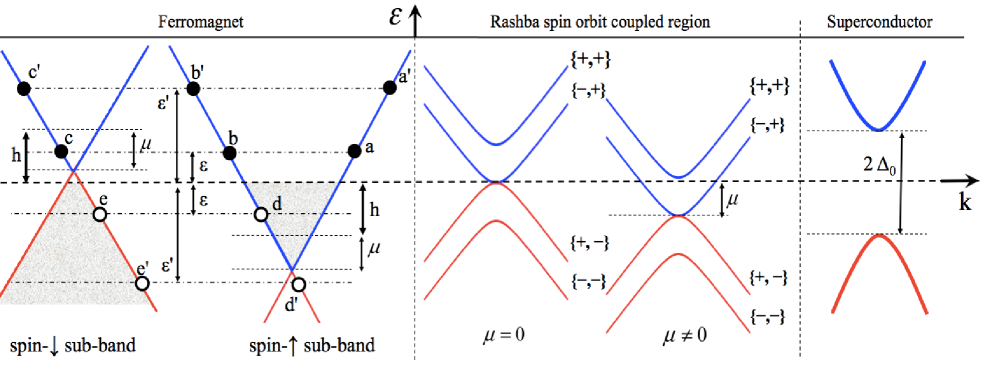
The electronic band structure of each region can provide helpful insights into the properties of system, particularly the various backscatterings and superconducting correlations. To obtain dispersion relations and corresponding spinors in each region, we diagonalize the DBdG Hamiltonian Eq. (1). The system band structure at low energies within F, RSO, and S regions can be expressed by:
| (5) |
| (6) |
where and
| (7) |
Figure 2 illustrates the excitation spectrums in the F, RSO, and S regions. The superconductor is assumed highly dopped so that the low energy excitation spectrum is a parabola. In our calculations of the reflection and transmission probabilities we consider a scenario where an electron with spin-up hits the F-RSO interface. Due to the tunable Fermi level in a graphene layer, one can consider three regimes: () undopped regime with , () low dopped limit with and () heavily dopped limit with . In the RSO region, the band structure has two subbands considering and () signs. Due to the subbands, the RSO region serves as a spin mixer in the transport mechanism. Therefore, when an electron with spin-up hits the F-RSO interface, there is a finite probability for a hole reflection with spin-up. The influence of and are shown in the F region. The solid circles show the holes in the bands and solid circles stand for the electrons. For a subgap electron with spin-up and , corresponding backscattering possibilities are labeled by -. The backscattering of is the normal electron reflection, is the normal spin-flipped, is the anomalous Andreev reflection where the backscattered hole lies in the conduction band, and is the conventional Andreev reflection where the backscattered hole passes through the valance band. We also show a case where the energy of incident electron takes a value of by - labels. In this case, the anomalous Andreev reflected hole passes through the valance band.
In an undopped graphene layer, the chemical potential is vanishingly small . Depending on the energy of incident particle, a new type of Andreev reflection can take place which is called specular Andreev reflection Beenakker . The specular Andreev reflection occurs when an electron in the conduction band is converted into a hole in the valence band upon the scattering process. It shows the possibility of an unusual electron-hole conversion in the reflection of relativistic electrons in graphene junctions Beenakker . In the retro Andreev reflection however electron and hole both lie in the conduction band as shown in Fig. 2. To gain more insights into various reflections that shall be discussed below, we have presented details of calculations and reflections in Appendix. In the low dopped regime (), by tuning the system parameters, novel effects can occur: () : In this limit, if the RSO parameter is zero (), the Rashba region acts similarly to a normal region with a finite width where the particles can experience resonances upon multiple reflections from boundaries. Hence, there are only two reflection probabilities present: ) conventional normal reflection () and ) either retro Andreev reflection () or specular Andreev reflection (), depending on the quasiparticle’s energy discussed above. The conventional normal reflection dominates at energies below the superconducting gap () Beenakker . In this regime, because and exchange field are equal, the population of spin-down electrons is minority and thus and has a finite probability. () At nonzero values of , a spin-up particle arriving from the F region, can undergo a spin mixing process in the RSO segment. In this limit, in addition to the normal reflection , the probabilities of anomalous Andreev reflection () and unconventional normal reflection () have finite amplitudes (see Appendix). Using this choice of parameters, the conventional Andreev reflected hole is placed in the valence band while the anomalous one passes through the conduction band. Moreover, a hole in the conduction band belongs to the retro-reflection process whereas a hole in the valence band belongs to the specular reflection mechanism Beenakker . Thus, the reflected holes can follow two different processes inside the F region depending on their spin orientation (see left panel of Fig.2). In a heavily dopped graphene , the Andreev reflection is of retro-type. The propagation of carriers are limited by critical angles that can describe their incident or reflection angles:
| (8) |
As seen, in a regime where , , the critical angles vanish. Therefore, their corresponding probabilities do not contribute to the quantum transport. Our investigations demonstrate that in a certain regime of parameter space where , the anomalous Andreev reflection highly dominates in the space. This regime results in zero conventional Andreev reflection while at the probability of anomalous Andreev reflection at the edge of superconducting gap becomes unity. This effect suggests a spin-polarized Andreev-Klein reflection zar1 . Note that the existence of phenomena described above are dependent on the presence of .
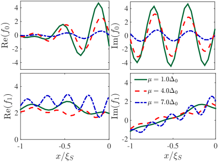
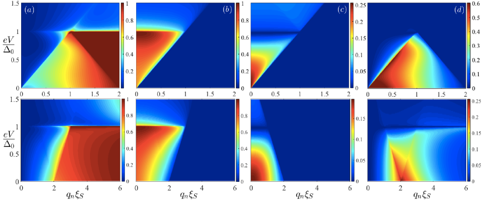
Figure 3 exhibits back scattering probabilities of an incident particle with spin-up at the F-RSO interface. Throughout our calculations, we consider a fairly narrow region that allows more clear analysis of the ESPs and anomalous Andreev reflection. In the top row panels we set the chemical potential at the superconducting gap and plot probabilities as a function of an applied voltage across the junction and the transverse particle’s momentum which is a conserved quantity during the scattering process throughout the system. Here we also consider corresponding to zero strain exertion into the system. As seen, in the presence of RSO region, an Andreev reflected hole with the same spin direction as the incident particle can occur with a finite probability. Furthermore, by calibrating , spin orbit coupling strength , and strain one can suppress the conventional Andreev reflection and simultaneously generate anomalous Andreev reflected holes with a finite probability. We note that is absent in uniformly magnetized junctions without the RSO region zar1 ; majidi ; chines . In Fig. 3 bottom row, we change to and . Comparing panels ()-(), we see that by tuning the Fermi level one can have a great control over a dominant reflection type at certain applied voltages. For instance, through our specific choice of parameters’ value, the anomalous Andreev is well separated from the standard Andreev and spin-filliped normal reflections. Hence, at low voltage differences across the junction, one can access a regime where the anomalous Andreev reflection is the highly dominated reflection simply by tuning the Fermi level. This interesting regime can be determined through a conductance experiment that shall be discussed later. Also, the results can be understood by the band structure analysis presented above and Eq. (8). Another experimentally controllable parameter that a graphene layer offers is the exertion of an external mechanical tension into the graphene sheet. Our results have found that strain can also change the Andreev and normal reflections the same as what was seen for and . That is, the strain can render the system to a regime where the anomalous Andreev reflection dominates. We now proceed to discuss the generation of triplet pairs and the properties of charge and spin conductances in a junction of F-RSO-S.
III.2 Equal- and opposite-spin pairings
It is of fundamental importance to find an experimentally feasible fashion to have control over the amplitude and creation of the equal-spin triplets. Such a control would help to unambiguously reveal the existence of such odd-frequency superconducting correlations in a hybrid structure. As discussed above, the RSO parameter is experimentally controlable through a simple external electric field ex1 ; ex2 ; ex3 . The graphene layers have also provided a unique opportunity to tune the Fermi level of a condensed matter system through applying a gate voltage. To further explore the relation between the anomalous Andreev reflections and triplet correlations, we calculate the opposite- and equal-spin pair correlations denoted by and halt1 ; halt2 ; halt3 . Following Ref. halt1, , the OSP and ESP in the graphene system we consider can be expressed by:
| (9) | |||
| (10) |
where and denote different valleys and stands for A and B sublattices halt1 . Here
| (11) |
in which is the relative time in the Heisenberg picture halt1 . Figure 4 illustrates the real and imaginary parts of OSP () and ESP () near the F-RSO interface in the ferromagnetic region shown in Fig. 1 i.e. . The different curves correspond to different Fermi levels equal to . We set the voltage difference across the junction fixed at whereas other parameters are identical to those of Fig. 3. When we set , the ESP vanishes and only remains nonzero. This is consistent with the known findings in a uniform ferromagnet coupled to a wave superconductor where the only nonvanishing triplet pairing is bergeret_rmp ; Buzdin2005RMP ; halt1 ; halt2 ; halt3 . A nonzero however results in a finite nonvanishing ESP in addition to the presence of . As seen in Fig. 3, for , by calibrating one can highly suppress the amplitude of OSP while increase . This finding is consistent with those of Ref. halt1, for a F-S-F contact with noncolinear magnetization alignments. This is however in stark oppose to a conventional metal counterpart where the tunable chemical potential is absent halt1 ; equalspin1 ; equalspin2 ; halt3 . We note that the amplitude of anomalous Andreev reflection discussed in Fig. 3 possesses identical aspects to the ESPs that demonstrates direct link of the equal-spin parings and the anomalous Andreev reflected holes.
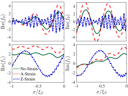
We also introduce two kinds of strain: Strain applied along the Armchair direction (-strain) and Zig-zag direction (-strain) i.e. and directions in Fig. 1, respectively. The applied tension into the graphene lattice causes anisotropic velocities in the and directions in each region : and aslo changes the coupling energy between carbon atoms eV. To model the - and -strain, we consider a strain strength of order of 20 which is equivalent to in our model (see Ref. Alidoust2011, ). In this amount of stress , the coupling energies change to and for the -strain while and for the -strain Alidoust2011 . Using these parameters, we calculate the corresponding anisotropic velocities of Dirac fermions in strained graphene lattice. Figure 5 exhibits the real and imaginary parts of and pair correlations in region for a strain-free junction and in the presence of - and -strain. For simplicity in analysis, we set identical strains in each region, the chemical potential is fixed at , exchange field , , and a voltage difference at across the junction. As seen, the amplitudes of OSPs and ESPs are highly influenced by the strain introduced. Interestingly, in the case of -strain, the amplitude of rapidly oscillates and diminishes while becomes less oscillating and smoother. This behaviour is suggestive of an experimentally feasible fashion to have control over the amplitude of both and so that one can suppress and simultaneously enhance in the same system. We have also investigated the back scattering amplitudes in the presence of strain (not shown). As one can expect, in the -strain mode, the anomalous Andreev reflection survives while the conventional Andreev reflection is vanishingly small that reaffirms the direct connection of and the anomalous equal-spin Andreev reflection.
III.3 Charge and spin conductances
An experimentally measurable quantity in such configuration is the junction conductance. Using the scattering coefficients, one can generalize the theory of Blonder-Tinkham-Klapwijkbtk to calculate the charge conductance via:
| (12) |
and the spin-polarized conductance:
| (13) |
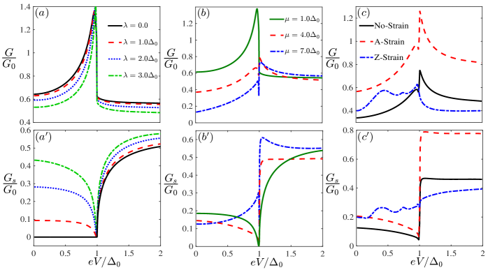
where and the junction width is assumed enough wide so that one can replace . The behaviour of normalized spin and charge conductances are shown in Fig. 6. We have normalized the conductances by . The presence of exchange energy in the F region results in an imbalance between particles with different spin directions and causes polarized currents at (black curve ). In the presence of RSO coupling however, due to the possibility of spin mixing in this region, the spin-polarized conductance can be also nonzero in the subgap region . The exchange energy and length of RSO region is kept fixed at and , respectively. Panels () and () illustrate the role of RSO in the charge and spin conductances. As seen, by increasing , the spin subgap conductance drastically enhances particularly at zero voltage bias while the associated charge conductance decreases. The enhancement of spin subgap conductance traces back to the generation of equal-spin triplet correlations (see Fig. 4, corresponding triplet correlations). Figure 6 also shows the effect of chemical potential in panels () and (). While the chemical potential can reduce the charge subgap conductance, the spin subgap conductance remains about the same at low voltages for the chosen set of parameters. The changes in the spin-polarized conductance is more pronounced at larger voltages. The influence of - and -strain is shown in () and (). We see that in the - strain mode the spin subgap conductance is almost largest while the corresponding charge conductance is less than -strain mode. The conductance behaviours are consistent with the associated backscattering probabilities and superconducting triplet correlations presented in the previous subsections.
IV conclusion
In conclusion, motivated by recent experiments avsar2014nat ; ex1 ; ex2 ; ex3 , we have theoretically studied backscattering probabilities, triplet superconducting correlations, and charge/spin conductance in a ferromagnet-Rashba spin orbit-superconductor graphene-based junction. Our findings offer an experimentally feasible platform for creating tunable superconducting equal-spin triplet correlations. The odd-frequency triplet correlations are formed near the F-RSO interface through an anomalous equal-spin Andreev backscattering. Considering the band structure of system, the anomalous reflection is allowed due to a band splitting in the presence of Rashba spin orbit coupling in the RSO region. We show that the amplitude of equal-spin pair correlations can be enhanced by varying the Fermi level in nonsuperconducting region, exertion of strain into the graphene layer, and controlling the strength of RSO through an external electric field while the amplitude of opposite-spin pair correlations suppressed simultaneously. The anomalous equal-spin Andreev reflection also causes a nonzero spin-polarized subgap conductance. These phenomena can be revealed in a conductance spectroscopy experiment. More importantly, the signatures of the equal-spin pairings on the experimentally observable quantities discussed here can supply suitable insights into the proximity-induced Rashba spin orbit couplings recently achieved in experiments avsar2014nat, ; ex1, ; ex2, ; ex3, .
Acknowledgements.
We thank M. Salehi for numerous helpful conversations. M.A. also would like to thank K. Halterman for useful discussions.V appendix
The wavefunctions associated with the dispersion relation in the F region are:
| (14) |
where represents a matrix with only zero entries and is a transpose operator. We assume that the junction width is enough large so that the component of the wavevector is a conserved quantity upon the scattering processes and therefore, we factored out the corresponding multiplication i.e. . The variables are the propagation angles in the presence of strain and are given by:
| (15) |
The superscript indicates electron (hole)-like parameters and subscript denotes the spin orientation. The component of wavevectors are not conserved during the scattering processes and can be expressed by:
| (16) |
We denote that can vary in interval . The component of the wavevector however becomes imaginary for larger values of than a critical value . The wavefunctions for are decaying functions and therefore, depending on the junction geometry, are not able to contribute to the transport process. The critical values can be expressed as follows:
| (17) |
In contrast to the intrinsic spin orbit couplings, the energy spectrum in the presence of RSO is gapless with a splitting of magnitude between subbands in the RSO region. The wavefunctions associated with the eigenvalues given in the text can be expressed by:
| (18) |
Here also the transverse component of wavevector is factored out due to the conservation discussion made earlier. The component of the wavevector however is not conserved during the scattering processes:
| (19) |
and the definition of auxiliary parameters are:
| (20) |
where are the electron and hole propagation angles in the region with spin orbit interaction. We note that if the transverse component of wavevector goes beyond a critical value , the same as what discussed for the ferromagnet region, the wavefunctions turn to evanescent modes. Here, however, since the RSO region is sandwiched between F and S regions, the evanescent modes contribute to the quantum transport process. We thus take both the propagating and decaying modes into account throughout our calculations.
In the superconductor region, denotes the electrostatic potential that is very large () in actual experiments compared to other system energy scales so that the step function assumption made above for the pair potential can be a good approximation in numerous realistic cases. The wavefunctions in the superconducting region are given by:
| (21) |
The parameter is responsible for the electron-hole conversions at the interface RSO-S and depends on the superconducting gap:
| (22) |
Similar expressions to those found for the longitudinal component of wavevector in the F and RSO region appear for the S. In the F region, we assume that a right moving electron with spin-up direction hits the interface of F-RSO with energy . This particle can reflect back as: (a) an electron with spin-up direction (conventional normal reflection), (b) as a hole with spin-down direction (conventional Andreev reflection), (c) as an electron with spin-down direction (spin flipped normal reflection), and (d) as a hole with spin-up direction (anomalous Andreev reflection). Thus, the total wavefunction in the F region can be written as:
| (23) |
where , , , and are the amplitudes of conventional, anomalous normal reflections, conventional, and anomalous Andreev reflections, respectively. When an electron hits the F-RSO interface, it can enter into the RSO region through one of its subbands and reflect back as an electron or hole upon collision with the RSO-S interface. Each subband is a mixture of spin-up and -down due to the presence of RSO coupling. Hence, in the RSO region, , the total wavefunction is given by:
| (24) |
As seen, the total wavefunction in this region involves 8 unknown coefficients for spin-up and -down particles and holes. Finally, the total wavefunction in the S region can be written as follows:
| (25) |
Here, the transmission coefficients are denoted by . The macroscopic phase of superconductivity plays no role in the geometry considered and thus we set it zero. In the above wave function, we assumed that the S region is in a heavily dopped regime i.e. . By matching the wavefunctions at the interfaces, i.e., at and at , we obtain the unknown scattering coefficients. The resulting coefficients however are very large and complicated expressions and we skip to present them.
References
- (1) A. I. Buzdin, Proximity effects in superconductor-ferromagnet heterostructures, Rev. Mod. Phys. 77, 935 (2005).
- (2) F. S. Bergeret, A. F. Volkov, and K. B. Efetov, Odd triplet superconductivity and related phenomena in superconductor-ferromagnet structures, Rev. Mod. Phys. 77, 1321 (2005).
- (3) M. Eschrig, Spin-polarized supercurrents for spintronics: a review of current progress, Rep. Prog. Phys. 78, 104501 (2015); M. Eschrig, Theory of Andreev Bound States in SFS Junctions and SF Proximity Devices, arXiv:1509.07818.
- (4) V. V. Ryazanov, V. A. Oboznov, A. Y. Rusanov, A. V. Veretennikov, A. A. Golubov, and J. Aarts, Coupling of two superconductors through a ferromagnet: evidence for a π junction, Phys. Rev. Lett. 86, 2427 (2001).
- (5) Ya. V. Fominov, A. A. Golubov, M. Yu. Kupriyanov, Triplet proximity effect in FSF trilayers, JETP Letters 77, 510 (2003); S. V. Bakurskiy, N. V. Klenov, I. I. Soloviev, M. Yu. Kupriyanov, A. A. Golubov, Superconducting phase domains for memory applications, Appl. Phys. Lett. 108, 042602 (2016).
- (6) M. Alidoust, K. Halterman, Proximity Induced Vortices and Long-Range Triplet Supercurrents in Ferromagnetic Josephson Junctions and Spin Valves, J. Appl. Phys. 117, 123906 (2015).
- (7) Y.N. Khaydukov, G.A. Ovsyannikov, A.E. Sheyerman, K.Y. Constantinian, L. Mustafa, T. Keller, M.A. UribeLaverde, Yu.V. Kislinskii, A.V. Shadrin, A. Kalabukhov, B. Keimer, D. Winkler, Evidence for spin-triplet superconducting correlations in metal-oxide heterostructures with noncollinear magnetization, Phys. Rev. B 90, 035130 (2014).
- (8) Y. Kalcheim, O. Millo, A. Di Bernardo, A. Pal, and J. W. A. Robinson, Inverse proximity effect at superconductorferromagnet interfaces: Evidence for induced triplet pairing in the superconductor, Phys. Rev. B 92, 060501(R) (2015).
- (9) K Halterman, M. Alidoust, Half-Metallic Superconducting Triplet Spin Valve, Phys. Rev. B 94, 064503 (2016).
- (10) M. G. Flokstra, N. Satchell, J. Kim, G. Burnell, P. J. Curran, S. J. Bending, J. F. K. Cooper, C. J. Kinane, S. Langridge, A. Isidori, N. Pugach, M. Eschrig, H. Luetkens, A. Suter, T. Prokscha and S. L. Lee, Remotely induced magnetism in a normal metal using a superconducting spin-valve, Nature Physics 12, 57 (2016).
- (11) I. V. Bobkova and A. M. Bobkov, Long-range proximity effect for opposite-spin pairs in superconductorferromagnet heterostructures under nonequilibrium quasiparticle distribution, Phys. Rev. Lett. 108, 197002 (2012).
- (12) P.D. Sacramento, L.C. Fernandes Silva, G.S. Nunes, M.A.N. Araujo and V.R. Vieira, Supercurrent-induced domain wall motion, Phys. Rev. B 83, 054403 (2011).
- (13) A. Moor, A. F. Volkov, K. B. Efetov, Nematic versus ferromagnetic spin filtering of triplet Cooper pairs in superconducting spintronics, Phys. Rev. B 92, 180506(R) (2015).
- (14) I. V. Bobkova and Yu. S. Barash, Effects of spin-orbit interaction on superconductor-ferromagnet heterostructures: Spontaneous electric and spin surface currents, JETP Lett. 80, 494 (2004)
- (15) F. Konschelle, I.V. Tokatly, F.S. Bergeret, Theory of the spin galvanic effect and the anomalous phase shift in superconductors and Josephson junctions with intrinsic spin orbit coupling, Phys. Rev. B 92, 125443 (2015).
- (16) F.S. Bergeret, I.V. Tokatly, Spin-orbit coupling as a source of long-range triplet proximity effect in superconductor-ferromagnet hybrid structures, Phys. Rev. B 89, 134517 (2014).
- (17) M. Alidoust and K. Halterman, Spontaneous edge accumulation of spin currents in finite-size two-dimensional diffusive spin–orbit coupled SFS heterostructures, New J. Phys. 17, 033001 (2015).
- (18) P. Hogl, A. Matos-Abiague, I. Zutic, and J. Fabian, Magnetoanisotropic Andreev Reflection in Ferromagnet-Superconductor Junctions, Phys. Rev. Lett. 115, 116601 (2015)
- (19) M. Alidoust and K. Halterman, Long-range spin-triplet correlations and edge spin currents in diffusive spin orbit coupled SNS hybrids with a single spin-active interface, J. Phys: Cond. Matt. 27, 235301 (2015).
- (20) G. C. Paul, P. Dutta, A. Saha, Transport and noise properties of a normal metal-superconductor-normal metal junction with mixed singlet and chiral triplet pairings, arXiv:1606.06270.
- (21) G. Tkachov, Magnetoelectric Andreev effect due to proximity-induced non-unitary triplet superconductivity in helical metals, arXiv:1607.05880.
- (22) A. H. Castro Neto, F. Guinea, N. M. R. Peres, K. S. Novoselov, and A. K. Geim, The electronic properties of graphene, Rev. Mod. Phys. 81, 109 (2009).
- (23) C.W.J. Beenakker, Andreev reflection and Klein tunneling in graphene, Rev. Mod. Phys. 80, 1337 (2008).
- (24) B. Z. Rameshti and M. Zareyan, Charge and spin Hall effect in spin chiral ferromagnetic graphene, Appl. Phys. Lett. 103, 132409 (2013).
- (25) N. Tombros, C. Jozsa, M. Popinciuc, H. T. Jonkman, and B. J. van Wees, Electronic spin transport and spin precession in single graphene layers at room temperature, Nature 448, 571 (2007).
- (26) X.-F. Wang and T. Chakraborty, Collective excitations of Dirac electrons in a graphene layer with spin orbit interactions, Phys. Rev. B 75, 033408 (2007).
- (27) H. B. Heersche, P. Jarillo-Herrero, J. B. Oostinga, L. M. K. Vandersypen, and A. F. Morpurgo, Induced superconductivity in graphene, Sol. Stat. Comm. 72, 143 (2007).
- (28) S. Dedkov, M. Fonin, U. Rudiger, and C. Laubschat, Rashba effect in the graphene/Ni (111) system, Phys. Rev. Lett. 100, 107602 (2008).
- (29) A. Varykhalov, D. Marchenko, M. R. Scholz, E. D. L. Rienks, T. K. Kim, G. Bihlmayer, J. Sa ̵́nchez-Barriga, and O. Rader, Ir (111) surface state with giant Rashba splitting persists under graphene in air, Phys. Rev. Lett. 108, 066804 (2012).
- (30) A. Avsar, J. Y. Tan, T. Taychatanapat, J. Balakrishnan, G.K.W. Koon, Y. Yeo, J. Lahiri, A. Carvalho, A. S. Rodin, E.C.T. O’Farrell, G. Eda, A. H. Castro Neto and B. Ozyilmaz, Spin orbit proximity effect in graphene, Nat.Commun., 5, 4875 (2014).
- (31) Z. Wang, C. Tang, R. Sachs, Y. Barlas, J. Shi, Proximity-induced ferromagnetism in graphene revealed by the anomalous Hall effect, Phys. Rev. Lett 114, 016603 (2015).
- (32) L. Razzaghi and M. V. Hosseini, Quantum transport of Dirac fermions in graphene with a spatially varying Rashba spin orbit coupling, Physica E 72, 89 (2015).
- (33) J. B. S. Mendes, O. Alves Santos, L. M. Meireles, R. G. Lacerda, L. H. Vilela-Leão, F. L. A. Machado, R. L. Rodríguez-Suárez, A. Azevedo, and S. M. Rezende, Spin-Current to Charge-Current Conversion and Magnetoresistance in a Hybrid Structure of Graphene and Yttrium Iron Garnet, Phys. Rev. Lett. 115, 226601 (2015).
- (34) S. Dushenko, H. Ago, K. Kawahara, T. Tsuda, S. Kuwabata, T. Takenobu, T. Shinjo, Y. Ando, and M. Shiraishi, Gate-Tunable Spin-Charge Conversion and the Role of Spin-Orbit Interaction in Graphene, Phys. Rev. Lett. 116, 166102 (2016).
- (35) V. Edelstein, Spin polarization of conduction electrons induced by electric current in two-dimensional asymmetric electron systems, Solid State Comm. 73, 233 (1990).
- (36) N. M. R. Peres, The transport properties of graphene: An introduction, Rev. Mod. Phys. 82, 2673 (2010).
- (37) V. M. Pereira, A. H. Castro Neto, and N. M. R. Peres, Tight-binding approach to uniaxial strain in graphene, Phys. Rev. B 80, 045401 (2009).
- (38) Y. Jiang, T. Low, K. Chang, M. I. Katsnelson, and F. Guinea, Generation of pure bulk valley current in graphene, Phys. Rev. Lett. 110, 046601 (2013).
- (39) M. M. Grujić, M. Z. Tadic, and F. M. Peeters, Spin-valley filtering in strained graphene structures with artificially induced carrier mass and spin-orbit coupling, Phys. Rev. Lett. 113, 046601 (2014),
- (40) J. L. Mañes, F. de Juan, M. Sturla, and M. A. H. Vozmediano, Generalized effective Hamiltonian for graphene under nonuniform strain, Phys. Rev. B 88, 155405 (2013).
- (41) J. Wang, K. S. Chan, and Z. Lin, Quantum pumping of valley current in strain engineered graphene, Appl. Phys. Lett. 104, 013105 (2014).
- (42) C. Benjamin, How to detect a genuine quantum pump effect in graphene?, Appl. Phys. Lett. 103, 043120 (2013).
- (43) G. J. Verbiest, S. Brinker, and C. Stampfer, Uniformity of the pseudomagnetic field in strained graphene, Phys. Rev. B 92, 075417 (2015).
- (44) M. Assili, S. Haddad, and W. Kang, Electric field-induced valley degeneracy lifting in uniaxial strained graphene: Evidence from magnetophonon resonance, Phys. Rev. B 91, 115422 (2015).
- (45) S. Zhu, J. A. Stroscio, and T. Li, Programmable Extreme Pseudomagnetic Fields in Graphene by a Uniaxial Stretch, Phys. Rev. Lett. 115, 245501 (2015).
- (46) R. Mohammadkhani, B. Abdollahipour, M. Alidoust, Strain-controlled spin and charge pumping in graphene devices via spin-orbit coupled barriers, EuroPhys. Lett. 111, 67005 (2015).
- (47) F. Sattari, Spin transport in graphene superlattice under strain, J. Mag. and Mag. Mat. 414, 19 (2016).
- (48) C.W.J. Beenakker, Specular Andreev reflection in graphene, Phys. Rev. Lett. 97, 067007 (2006).
- (49) K. Halterman, O. Valls, and M. Alidoust, Spin-controlled superconductivity and tunable triplet correlations in graphene nanostructures, Phys. Rev. Lett. 111 046602 (2013).
- (50) K. Halterman, O. T. Valls, and M. Alidoust, Characteristic energies, transition temperatures, and switching effects in clean SNS graphene nanostructures, Phys. Rev. B 84, 064509 (2011).
- (51) M. Alidoust and J. Linder, Tunable supercurrent at the charge neutrality point via strained graphene junctions, Phys. Rev. B 84, 035407 (2011).
- (52) M. Zareyan, H. Mohammadpour, and A. G. Moghaddam, Andreev-Klein reflection in graphene ferromagnet-superconductor junctions, Phys. Rev. B 78, 193406 (2008).
- (53) Y. S. Ang, L. K. Ang, C. Zhang, and Z. Ma, Nonlocal transistor based on pure crossed Andreev reflection in a EuO-graphene/superconductor hybrid structure, Phys. Rev. B93, 041422(R) (2016).
- (54) L. Majidi and R. Asgari, Valley-and spin-switch effects in molybdenum disulfide superconducting spin valve, Phys. Rev. B 90, 165440 (2014).
- (55) K. Halterman, P. H. Barsic, and O. T. Valls, Odd triplet pairing in clean superconductor/ferromagnet heterostructures, Phys. Rev. Lett. 99, 127002 (2007).
- (56) K. Halterman, O. T. Valls, and P. H. Barsic, Induced triplet pairing in clean s-wave superconductor/ferromagnet layered structures, Phys. Rev. B 77, 174511 (2008).
- (57) C. Visani, Z. Sefrioui, J. Tornos, C. Leon, J. Briatico, M. Bibes, A. Barthelemy, J. Santamaria, and Javier E. Villegas, Equal-spin Andreev reflection and long-range coherent transport in high-temperature superconductor-half metallic ferromagnet junctions, Nature Phys. 8, 539 (2012).
- (58) X. Wu, H. Meng, Gate-voltage control of equal-spin Andreev reflection in half metal-semiconductor-superconductor junctions, Phys. Lett. A 380, 1672 (2016).
- (59) G. E. Blonder, M. Tinkham, and T. M. Klapwijk, Transition from metallic to tunneling regimes in superconducting microconstrictions: Excess current, charge imbalance, and supercurrent conversion, Phys. Rev. B 25, 4515 (1982).
- (60) M. Salehi and G. Rashedi, Spin-polarized conductance in graphene-based FSF junctions, Physica C 470, 703 (2010).